IMECODER FOR NEUTRON
*«"
»Kiil·
zwm
\¡,i fiCil iiti ΗΗΕΠ]
i'HiFfWjT'
»
f+vBfc.|| « »'Vi! :.ι. allittiiiJUlllïMüSj»3rt: «Γ* jlilrlüliÜillíriüSSl.ílü'tír'fci!·
ΡίίίΐΡδ4«ΙνΛ,
,i!;tAUi:Tíif'Í''Pi.ilí-*-í-.>«,.·:! τlHeit
'
staDnsnnuMU-
öe,"
,uml i i
ral Bureau for Nuclear Measurements-CBNM
its contractors
make any warranty or representation, express or implied, with respect to the accuracy, completeness, or usefulness of the information contained in this document, or that the use of any information, apparatus, method,
Afifei
EUR 4835 e
A T I M E C O D E R FOR N E U T R O N T I M E - O F - F L I G H T EXPERIMENTS by S. DE J O N G E
Commission of the European Communities
Joint Nuclear Research Centre — Geel Establishment (Belgium) Central Bureau for Nuclear Measurements — CBNM
Luxembourg, May 1972 — 20 Pages — 9 Figures — B.Fr. 40.—
The described timecoder is designed for neutron time-of-flight experiments at the linear accelerator of the CBNM at Geel, Belgium.
By the use of MECL II integrated circuits it features simple design and low cost. Basic channelwidth is 40 ns, which can be multiplied in 8 succeeding regions with a factor of 1 to 99, which may be different for each region. In regions where no events have to be stored, address counting is inhibited which results in optimal use of the 4096 output channels (12 bits).
The deadtime of the coder together with a buffer memory is 280 ns, permitting several events to be registered during one measurement cycle.
EUR 4835 e
A T I M E C O D E R F O R N E U T R O N T I M E - O F - F L I G H T EXPERIMENTS by S. D E J O N G E
Commission of the European Communities
Joint Nuclear Research Centre — Geel Establishment (Belgium) Central Bureau for Nuclear Measurements — CBNM
Luxembourg, May 1972 — 20 Pages — 9 Figures — B.Fr. 40.—
The described timecoder is designed for neutron time-of-flight experiments at the linear accelerator of the CBNM at Geel, Belgium.
By the use of MECL II integrated circuits it features simple design and low cost. Basic channelwidth is 40 ns, which can be multiplied in 8 succeeding regions with a factor of 1 to 99, which may be different for each region. In regions where no events have to be stored, address counting is inhibited which results in optimal use of the 4096 output channels (12 bits).
The deadtime of the coder together with a buffer memory is 280 ns, permitting several events to be registered during one measurement cycle.
EUR 4835 e
A T I M E C O D E R FOR N E U T R O N T I M E - O F - F L I G H T EXPERIMENTS by S. DE J O N G E
Commission of the European Communities
Joint Nuclear Research Centre — Geel Establishment (Belgium) Central Bureau for Nuclear Measurements — CBNM
Luxembourg, May 1972 — 20 Pages — 9 Figures — B.Fr. 40.—
The described timecoder is designed for neutron time-of-flight experiments at the linear accelerator of the CBNM at Geel, Belgium.
By the use of MECL II integrated circuits it features simple design and low cost. Basic channelwidth is 40 ns, which can be multiplied in 8 succeeding regions with a factor of 1 to 99, which may be different for each region. In regions where no events have to be stored, address counting is inhibited which results in optimal use of the 4096 output channels (12 bits).
EUR 4835 e
COMMISSION OF THE EUROPEAN COMMUNITIES
A TIMECODER FOR NEUTRON
TIME-OF-FLIGHT EXPERIMENTS
by
S. DE JONGE
1972
Joint Nuclear Research Centre Geel Establishment-Belgium
ABSTRACT
The described timecoder is designed for neutron time-of-flight experiments at the linear accelerator of the CBNM at Geel, Belgium.
By the use of MECL II integrated circuits it features simple design and low cost. Basic channelwidth is 40 ns, which can be multiplied in 8 succeeding regions with a factor of 1 to 99, which may be different for each region. In regions where no events have to be stored, address counting is inhibited which results in optimal use of the 4096 output channels (12 bits).
The deadtime of the coder together with a buffer memory is 280 ns, permitting several events to be registered during one measurement cycle.
KEYWORDS
TIME OF FLIGHT METHOD LINEAR ACCELERATORS DEAD TIME
CONTENTS *)
P ag e
1. Design considerations 5
2. Realised specifications 5
3. Simplified logic d i a g r a m 6
4. Circuit description 8
4. 1. Clock oscillator 8
4. 2. CW counter 8
4. 3. ZL counter 9
4. 4. Address and phasing 1 9
4. 5. A d d r e s s and phasing 2 11
5. Conclusions 11
5
-A TIMECODER FOR NEUTRON TIME-OF-FLIGHT EXPERIMENTS 1. DESIGN CONSIDERATIONS
In o r d e r to make efficient us£ of m e m o r y storage in neutron t i m e -of-flight experiments the channelwidth is increased when flight
time i n c r e a s e s , keeping the neutron energy resolution about constant. Neutron energies of several MeV's down to 0. 025 eV corresponding to flight t i m e s of 0. 5 /us up to 45 m s on a 100 m e t e r flight path, have to be analysed and stored in a 12 bit (409 6 channels) m e m o r y .
To meet the above mentioned r e q u i r e m e n t s the timecoder should have 8 zones within one m e a s u r e m e n t cycle, where it should be possible to multiply the basic channelwidth with a factor of 1 to 99.
One or m o r e of these zones could be zones without interesting events, where storage has to be inhibited (Fig. 1 and 2). The minimum
channelwidth determines the resolution and as special equipment is available for higher resolution m e a s u r e m e n t s 40 ns is to be considered as sufficient at the CBNM Linac.
P r e c i s i o n and stability of this basic channelwidth have to be better than 10" 5 a figure being determined by the timing uncertainty at the neutron source. A normal quartz crystal in the clock oscillator m e e t s these r e q u i r e m e n t s .
Differential linearity of the coder should be better than 1%. This implies that the channels should be of equal width. Careful lay-out and decoupling of the phasing circuits for the TQ- and Τ -signals
will keep the threshold of these circuits constant and no timing e r r o r s will occur.
As several operations such as opening and closing of m e a s u r e m e n t zones, readout of a d d r e s s scaler e t c . , have to be performed within one clock period fast switching elements should be used. MECL II circuits with a propagation delay of 2 - 9 ns will be suitable.
2. REALISED SPECIFICATIONS Channelwidth: 40 ns ,
P r e c i s i o n : 5.10 Stability: 1. 10"6
Differential linearity: 0. 5% Number of zones: 8 Minimum zone length: 400 ns Deadtime: 280 ns Maximum range: 320 m s
6
-3. SIMPLIFIED LOGIC DIAGRAM (Fig. 3)
Under n o r m a l working conditions t h e r e a r e 2 inputs; a TQ s i g n a l
which s t a r t s the t i m e c o d e r p r o g r a m and a Τ signal being the event of which the t i m e Tn T0 h a s to be coded. A t h i r d input
( P r e t r i g g e r ) can eventually be used as a safety r e s e t .
At the a r r i v a l of the p r e t r i g g e r , r e s e t OS 1 i s fired r e s e t t i n g the following c i r c u i t s : T0F F , zone s c a l e r , CW counter, ZL
counter and a d d r e s s s c a l e r . It should be noticed that the zone s c a l e r is r e s e t to position 111, which i s decoded and the f i r s t group of digitswitches is selected by the level a d a p t e r .
A group of digitswitches c o n s i s t s of:
1. A sign switch, which indicates whether events should be r e corded (+ - "ZD) or not ( = ZD) in the concerning zone. 2. Two d e c a d e s indicating the channelwidth multiplication
factor.
3. F o u r d e c a d e s indicating the zone length in n u m b e r of c h a n n e l s .
The r e s e t pulse p a s s i n g through OR gate 1 t r a n s f e r s ZD or ZD into the Z D F F and the channelwidth multiplication f a c t o r into the CW r e g i s t e r .
After the r e s e t pulse h a s o c c u r r e d a pulse is g e n e r a t e d by the c i r c u i t called "Shaping" and through OR gate 2 the zone length is t r a n s f e r r e d into the zone length counter by AND gate 3. Also a clock pulse i s fed to the zone s c a l e r , causing its p o s i tion change to 000 and the second group of digitswitches is
s e l e c t e d .
At the s a m e t i m e the channelwidth from the channelwidth r e g i s t e r i s t r a n s f e r r e d into the channelwidth counter by AND gate 5. When Τ a r r i v e s the flipflop TQF F i s set. Next the
output of Τ F F is brought in phase with the clock in such a way, that the clock gates 6 and 7 a r e opened just inbetween two clock p u l s e s . This phasing is done in TQF F T D , which i s
a tunneldiode flipflop. A MECL II flipflop, giving a t u r n o n delay up to 30 ns for s m a l l o v e r l a p between set and clock pulse, cannot be used for t h i s p u r p o s e , as the t r i g g e r d e l a y should be l e s s than half a clock p e r i o d (20 n s ) .
The CW counter, a BCD downcounter, is driven now by clock p u l s e s and e v e r y t i m e the counter a r r i v e s at position 00 one clock pulse is fed through overflow gate 8. This overflow p e r f o r m s the t h r e e following functions:
1. The channelwidth multiplication factor which is still in the CW r e g i s t e r is t r a n s f e r r e d again in the CW counter.
2. The a d d r e s s s c a l e r is driven with clock p u l s e s by gate 9, when events should be r e c o r d e d in the f i r s t zòne.
7
-The ZL counter is a 4 decade BCD downcounter. When this counter r e a c h e s position 0000, an overflow is generated, which t r a n s f e r s through gate 2 the length of zone 2 into the ZL counter. At the same time the channelwidth multiplica tion factor and the information "Zone Dead" or "Zone Dead" for zone 2 a r e t r a n s f e r r e d into the CW r e g i s t e r and Z D F F .
The zone scaler advances to position 001 selecting digitswitch group 3.
The propagation delay in zone scaler - decoder - level adapter i n s u r e s that this advance in selection does not occur too e a r l y and limits at the same time the minimum zone length to 400 n s . This p r o c e s s goes on until the last zone is reached, selected by the digitswitch "Number of Zones", which enables gate 11. The next overflow of the ZL counter fires r e s e t OS 2, which closes the t r a n s f e r gate 12 and at the same time t r i g g e r s r e s e t OS 1. The p r o g r a m which was selected on the digit-switches is ended and the coder r e t u r n s to its original state. The three bit output of the zone scaler can be used as routing inputs for the a d d r e s s r e g i s t e r , so that every coded event is accompanied by the number of the zone in -which the event o c c u r r e d .
The events of which the flight time have to be m e a s u r e d ( Tn- T )
enter through gate 13, which is normally open.
The Tn flip-flop is set by the leading edge of this signal and
further phased with the clock in such a way, that the t r a n s f e r gate 12 opens inbetween two clock p u l s e s . TnF F and TQFFTD
a r e self resetting after 40 ns.
If the event falls in a zone in which it should be r e g i s t e r e d , the t r a n s f e r gate is enabled by the level Zone Dead.
The transfer flip-flop is set, which on its turn closes the t r a n s f e r gate and the input gate 13 through OR gate 14.
The single output pulse of the t r a n s f e r gate strobes the a d d r e s s r e g i s t e r , which takes its binary coded time information from the a d d r e s s s c a l e r .
The a d d r e s s scaler is read in flight inbetween two clock p u l s e s . The state of the t r a n s f e r flip-flop indicates that the coder is ready.
The output adapter or buffer store sequencially reads the a d d r e s s and generates a r e s e t . This r e s e t signal r e s e t s the t r a n s f e r flip-flop and at the same time keeps the input gate
- 8
4. CIRCUIT DESCRIPTION
4 . 1 . Clock oscillator (Fig. 4)
The clock oscillator is a 25 MHz overtone oscillator (l) con-structed with l / 4 MCI 010. Capacitors C, and C¿ a r e giving a certain ratio between clock-up time and clock-down time for the two outputs, assuring proper timing in the CW counter and phasing flip-flops.
4 . 2 . CW counter (Fig. 4 and Fig. 9)
The CW counter is a p r o g r a m m a b l e two decade BCD down counter (2) constructed with J-K flip-flops of the type MCI01 3. The dividing factor (1 to 99) can be set into the counter from the r e g i s t e r 4E-4H. When clock gate 6Da is open (T F F is true)
clock pulses a r r i v e from 6D-6.
Overflows of the l e a s t significant digit a r e detected by gate 8F , the output of which s e r v e s as the clock input for the preceding decade. Gate 8FIL detects the overflow of this decade. If an overflow occurs the clock line is inhibited and at the same time gate 8E is enabled at input 10.
F u r t h e r m o r e gate 8E gives an output when the least significant decade a r r i v e s at position 0001. Its clock line is inhibited and gate oD-tø is opened with delay, caused by RQ and the gate input capacitance.
The next clock pulse, occurring at the time at which the contents of the whole scaler would be zero, is passing through and t r a n s -fers the contents of the CW r e g i s t e r again into the s c a l e r . These cycles continue Until clock gate 6D c l o s e s .
The first stage of the scaler (6F) has double steering, as it does not r e t u r n to zero, which is the case for the other stages. When data a r e t r a n s f e r r e d into the scaler, spurious pulses can occur at the clock line of the second decade, caused by differences in propagation delay in the scaler stages. The clock line is de-coupled with 82 pf to suppress these p u l s e s .
The r e s e t line, which is distributed throughout the coder, enters through a low pass filter, to improve the noise immunity.
Before a m e a s u r e m e n t cycle s t a r t s the information of the CW r e g i s t e r is t r a n s f e r r e d into the CW counter by signal JB} As the S and R input of the J-K flip-flop (MCI013) do not always dominate the J-K inputs, the clock lines have to be kept high during setting and resetting. When not, some decades
start oscillating during this action, resulting in a faulty scaler contents.
9
(wired AND) by the output of the Zone Dead flipflop (ZDFF). The ZDFF is driven with delay from another flipflop for proper timing. The outputs Gated Clock and ZD are respecti vely used as clock input and enable input of the transfer gate. Level TQFF opens the clock gates at the beginning of a mea
surement cycle.
4. 3. ZL counter (Fig. 5 and Fig. 9)
The ZL counter is a 5 decade BCD down counter and is built up in the same way as the CW counter.
The output pulse QU appearing at gate 5D6 after the trailing edge of the reset pulse transfers through gate 5C the contents of the first group of digitswitches, indicating the zone length.
The ZL counter has the following outputs:
1. FST BIN, which is the output of the first counter stage and used for monitoring as discussed later.
2. ZONE OFLO, with functions:
a. Transfer of the sign (ZD or ZD) of the digitswitch into the Ζ D flipflop.
b. Advance of the zone scaler.
c. Termination of the measurement cycle if the selected number of zones is reached.
3. XFER CW, appearing just before the end of a zone, which transfers the channel width of the next zone into the CW register.
Several lines on the printed circuit board are longer than 7 cm, what causes ringing after transients. To damp these oscilla tions the longer lines are terminated with a voltage divider of 2 χ 220 Ω between supply voltage and ground.
This method gives rise to a decreased noise immunity as the gate output voltags swing decreases. In practice however no problems occurred in connection with this effect.
4.4. Address & Phasing 1 (Fig. 6)
The zone counter consists of a three stage binary counter, constructed with JK flipflops. Its outputs are decoded and these are amplified by 8 identical level adapters (T, and T?) to levels between GND and 5V. These outputs serve as the
selection level of the 8 groups of digitswitches.
As the BCD outputs of the digitswitches are diode ORed it is not possible to select the switches with the MECLII level, because of the diode voltage drop.
The negative start pulse for the coder (T ) enters through level adapter T¿4 and sets flipflop 6F.
Δ ^ · VEE(Vdl+Vd2) _ . . .
A current 1 π » ■ u = 3. 3 mA is switched into
- 10
the tunneldiode. (Re is the internal emitter r e s i s t o r of 6F, being 1K5). If now a clock pulse occurs, or was already p r e s e n t from 6E-11, a c u r r e n t of 3 mA is added and the tun-neldiode switches to its high state.
When flip-flop 6F is reset, the tunneldiode r e s e t s at the same time because it has voltage drive for positive t r a n s i -tions of the preceding flip-flop. The diode D1 adds ~ 0 . 7 5 V
to the tunneldiode voltage and brings i t just to MECLII levels. The width of the clock pulse is l e s s than 20 ns, so that the time jitter on the phased signal is l e s s than 20 ns with r e s p e c t to the clock. This fact allows the clock gates of the CW coun-t e r coun-to be opened juscoun-t inbecoun-tween coun-two clock pulses by coun-the signal
T0F F .
The used phasing method which is the same for the events (T ) causes triangular time channels with a width of 40 ns on half height. When the channel width multiplication factor is g r e a t e r than 1 the time channels have a trapezoidal shape.
The output of the Tn flip-flop ( TnF F ) is fed through a s e r i e s
of 4 i n v e r t e r s (6C), acting as a delay, in o r d e r to obtain the proper phase relation with the clock at gate 6 D - 1 .
The r e s e t signal which enters at IB is at TTL levels and adapted to MECLII levels by T^o. The r e s e t input signal at gate 6A-4 is slowed down to such an extent that the output of gate 6A-6 has a r i s e time of 40 ns, when an input (T ) was present during resetting.
The drive at the set input of TnF F is insufficient and r e g i s t r a
-tion of an input signal having no proper timing is prevented. If an event has to be r e g i s t e r e d the first clock pulse p a s s e s through gate 6Da (for conditions: TnFF."ZTJ. RESET. X F E R F F )
and sets the t r a n s f e r flip-flop, which on its turn closes gate 6Da and the input gate of TnF F . R e s i s t o r R40> together with
the gate input capacitance is acting as a delay, in o r d e r to keep gate 6Da open, long enough to have a whole clock pulse
passing through. This single pulse t r a n s f e r s the contents of the a d d r e s s scaler into the output r e g i s t e r .
The r e s e t one shot (3) which t e r m i n a t e s the m e a s u r e m e n t cycle consists of gate 6 Ea and oD^. It is enabled by the
level from digitswitch "NO OF ZONES" (DSg ) and is fired by the zone overflow. Enabling occurs also when the con-cerning digitswitch is in position 8 during the r e s e t cycle of the coder. As the zone overflow is p r e s e n t at the trailing edge of the r e s e t signal the gating level T F F is n e c e s s a r y to prevent firing at this t i m e .
The a d d r e s s and phasing 1 circuit has three outputs for external use:
1. READY, a level which indicates that coding of an event has taken place and the output a d d r e s s is available. 2. ZI (zone of interest), a level which is only present
during the time that events have to be accepted. 3. PR (program), a signal for monitoring on an o s c i l
11
-4. 5. Address fa Phasing 2 (Fig. 7)
The a d d r e s s scaler is a twelve bit synchronous binary counter constructed with J-K flip-flops of the type MCI 01 3. Coupling between the groups of stages is done with clock gates of the type MCI 023, keeping the propagation delay of the J-K con ditions to a minimum, (tpd MC1013 + 3.tpd MCI 023 = 15 ns).
The signal XFER ADDR, arriving between a d d r e s s scaler contents n and n+1 t r a n s f e r s the a d d r e s s n into the a d d r e s s r e g i s t e r 5A - 3A, composed of D flip-flops. On the command READ the information appears on the output lines in DTL l e v e l s .
The a d d r e s s r e g i s t e r contains 4 bits which can be used either for routing purposes (switches on external) or for indication of the zone a d d r e s s (switches on internal.
The r e s e t signal for the timecoder is delivered by the one shot IH and distributed to all counters.
The input PT (pretrigger) is an external r e s e t input, which may serve as a safety r e s e t , preceding every start pulse<T0).
5. CONCLUSIONS
Partition of time-of-flight spectra in different zones with different channel width can be done in the timecoder itself. The quantity of hardware is considerably reduced, compared with systems where coding is done first in a coder and p a r t i tion and channelwidth multiplication in a conditioner (4). In high frequency logic c i r c u i t r y like the h e r e described timecoder MECLII integrated circuits have proved to be attractive building blocks. Due to the low propagation delay there a r e little or no timing problems encountered, what allows relatively simple and straight forward logic design. F o r prints of a reasonable size (timecoder: 170 χ 280 mm) double-sided printed circuits can be used, if the supply ground is connected to the integrated circuits by a stripline (see fig. 9).
Ringing on long signal lines causes a problem, which can be solved either by parallel r e s i s t o r s or by s e r i e s r e s i s t o r s (5). The first method has the disadvantage of d e c r e a s e d noise immunity, the second one causes a significant i n c r e a s e in connections on the printed circuit board.
12
-REFERENCES
(1) Motorola application note AN 417. IC crystal controlled o s c i l l a t o r s .
(2) Motorola application note AN 456.
A 50 MHz p r o g r a m m a b l e counter designed with MECLII integrated c i r c u i t s .
(3) Motorola application note AN 233.
Design of monostable multivibrators using MECL integrated c i r c u i t s .
(4) F . Colling and W.Stttber, Nucl. Instr. and Meth. _64 (1968) N° 1.
A conditioner with integrated circuits for neutron time-of-flight experiment data selection.
(5) Motorola application note AN 277.
Overshoot and ringing in high speed digital s y s t e m s .
LIST OF FIGURES
Fig. 1: Timecoder programmation for the spectrum of Fig. 2. 238
Fig. 2: T r a n s m i s s i o n spectrum of Mn+U (20 - 300 eV).
Fig. 3: Timecoder simplified diagram.
Fig. 4: CW & ZL counter 1.
Fig. 5: CW & ZL counter 2.
Fig. 6: Address & Phasing 1.
Fig. 7: A d d r e s s & Phasing 2.
F i g . 8: Frontview of the timecoder.
CHANNELWIDTH MULTIPLICATION
ADDRESS
13
-NO. OF CHANNELS
Figi TIMECODER PROGRAMMATION FOR THE SPECTRUM OF FIG.2
4000-1
to
2 =5 O
0 64 2112
CHANNEL NUMBER
ι 1
r-r-4096
'n LT 0.7 wv
PREU
O — \ . J>-* IRESET O.S. 1
l ^ n
Li-I
To LT
O
Î
TnFF Q STnFF TD XFER GATE ICLÕCK CLOCK "3~ 3«ITSW NO.
ZON
Î)
RESETO.S. 2
O
α
ZONE ADDRESS
^E>
T0FF Q S
T0 FF _5 TD J ICLOCK
XFER CW SET ZL
8 * I F
¿£>
CLOCIKÎJ
SHAPING SET CW ~1>ïtearv LU
CLOCK
<jp;
CLOCK 25 HC
^ >
ZD GATE
XFER
FF
t>
< l ·
CLOCK ADDRESS SCALER 12 BITS _ ^ RESET
■—CLOCK ADDRESSREGISTER 1 2 . 4 BITS
LINE DRIVERS
Ö
V
V
OUTPUT ADAPTER
I LI I 16 BITS ♦ XFER
CW CHANNEL WIDTH ZL ZONE LENGTH ZD ZONE DEAD
ROUTING
V
ROUTING
< l ·
Q READ
OS Ιμ«
OS 19 μ ι
1' / ι
■Ε
Ι
EVENT
i WORD BUFFER STORE
J
Fig.3 TIMECODER
15
-(MA)
2
(»À]
R,Mlk
» 4E 10
"CU
Θ
(¡à
Ï
5 4 E 4Í
» 4F MÏ
5 4 F 106A:
2
[ISA:
"Ï"
a 4G 10 S 4 G 44
Θ
6
(OÀ]
ij5~
s 4H 10ï
5 4 H^
■^®^d
:=&^d
:dB»-Rl9
-
ψ
220 RieRESET
Ξ
K K K J J J
T T t T Τ ι 211 10 β 5 4 3
6F 12j
;Jg^d
:=©^d
;dB^d
@—§
-—=E ii β io
5
t a s2 7E 6
12 'C 9
13 ~ 5 =
T i , τ ,1 Γ
11 ï 10 5 3 4
6F
=. l τ ι
11 8 10 5 3 4
2 7F β
121 'r 13 9
X
'M. DK) T T T T T T
11 10 B 5 3 4
2 cr 6
12 6 G 9
13
±=fc 11 β 10 4 3 5 7G
T l , . I 11 β 10 5 3 4
13 =1=
3 Ι Τ Ι Ξ
11 8 Μ 5 3 4
« Ή ;
1 13
Ι "■= 1013
Ù
C6560 ^ 1 4 7 0
8FQ J »04
82 C7
[ 5 G Ì I 0 2 3
42
-Ξ
CW OFLOQ
Θ
6Db
Ro
1023 [ 6DQ
E
220R20
Π 2 2 0 ΥΚ21
ZD
Q
-Θ
ADOR.CLOCK 102312A) GATED CLOCK
H A ) TOFF
13 12 7D 9 M
Γ®
ZDZDFF
ΗΗΠ
'°P Ik C. M o .7D 5 4
"E
ZD
R23T
DS
5A) CLOCK
D
internal connectionFig.4 CW & ZL COUNTER 1
- 16
IJ1—'
2 (35Α>
@-r-@-r-=ìgy
Hl
TftTW ι (32À>'=52^
;:*
2C© ^ r - ^
@rA*
R30U
Β ff///
@ H r ^ >
hU (28A> 2 (27A) Τ33Ι 4 (26A> «34 8 (2sÀ>
3~
«3«Π2 » n r
2 (23A] R37[] 4 ftrtw (22 8 (2ÍÃ; «38 ¡H>A
_ Rt 0
220
1
(S^-T-H
■»ote
Twtw unti
K K K J J J ¿ Ι X) 8 5 4 3
2A
12j l í
ï — «
3 F > ! L
-'Φ^— :i
:=£>* ;
^ —
Z i ,
', ~~§^ 2 2G
■Φ^:;
n ^ — = k
a=t 11 β
ñ - f
2 3A
» E _l Κ43Π220
Τ I ^ 4 F
11 8 10 5 3 4.
2B
=, r-r
11 8 10 5 3 4 3B
411
riC now
« » « » »
11 X) 8 S 4 à
t t
3
It β 10 4 3 5
I
2 3C
« 13
Τ I ^ 4 - t
11 8 10 5 3 4 2D
π r r
11 8 10 5 3 4 2 3D '
i p B11
LE)
10101001
= j*H
Jig))!L
0 [B]
1023
1023
3I<3 5] R48 SB 1 1023
220 1*46
CZrf « n F
3TF « » » '
3 220 ^ R47
4A I 1004 8 5 4 3
2E [
13
±=a= η c
11 β 10 4 3 5
3E
Τ 1 r*4F
11 8 10 5 3 4
2F
±=L J = t II 8 W 5 3 4.
3F
[CJCWOFLO [ Ï ] | N | I L I
TOFF RESET
4B
82
c9
1001
12 O
' I G S 1010
τ t t t t ι
11 β 10 5 4 3 13
arfc Π 11 β 10 4 3 5
SG
τ 1 Γott
11 β 10 5 3 4
2 2Η '2
a=L j = t ±
11 8 10 5 3 4 I 3H ι !1 L 1013 13 4C 82 cío ' * #
4 D I 1004
IG Ì 'οίο
4D 1004 82 Cil
.-*@J
-Ξ
DA) ES
, ZONE OF EO
(5DS 1010 5 10
HH
Cl2
-E
XFERCW
internal connection
Fig.5 CW & ZL COUNTER 2
ZONE OFLO 17
-8 11 10 5 4 3 t
H2 IE
K K K J J J
T T T T τ I
β 11 10 S 4 3 ι
IF 9 - " Κ
t - »
S
Έ
3
β 11 10 5 4 3.Η 2 ID 6-c>
220 R, 220 R44 "65 270
Î
«66 56020fl WTtTT
m
1043 β 9 10 11 IC 12 13 3 4AMPfNj'S Tu
ΐ>
Α Μ Ρ Γ \ ! ! 3 _ Τ 1 4 _ΐ>
ΐ>
Til τ «ΐ ^
Tíoΐ>
A M P [ \ T 7 _ T gAMPI
ΑΜΡΓ"\Τ3Τ4Ι^Τ5Τ6
1>
DS2
gp^-gJ8 Τ, FF ,3
"-Y-1 ""AS 1023
1 78
XFER
1010
1014 R6 e[ j3 k 3 1010
ZD 1023 3ç_ 6B XFER FF
JOt^^^S
47θΠ«β3 1014Q
"62m
TOFF1010 1039 R
, J M J
7s[> Z I16GJ »10
3^6H t
S!
«78 560
560
-CD-D
internal connection 1039Fig.6 ADDRESS & PHASING 1
internal connection
Fig.7 ADDRESS & PHASING 2
NEGATIVE LOGIC
19
-mmm -mmm
m
.JTfyrrFi ...y-mpi ...ρ
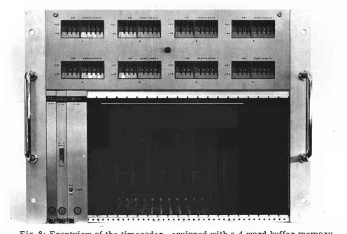
F i g . 8: Frontview of the timecoder, equipped with a 4 word buffer m e m o r y . Spare slots a r e available for input or output electronics.
[image:23.595.58.555.63.398.2]Sí.'aawjsfli'finTnr
kñw'
mÊmmm
NOTICE TO THE READER
scientific and technical reports published by the Commission the European Communities are announced in the monthly iodical "euro-abstracts". For subscription (1 year: B.Fr. 1025) free specimen copies please write to:
'IHjrajjff
of the European Communities P.O. Box 1003
Luxembourg 1
(Grand-Duchy of Luxembourg)
I _
J Ä ;
a-Maffia
©111'«Ι»;-lil« It'lli
íiipílliJfÉllil
^sfetí
TMT'
4^
TSMtói'!iBn
ai
i l
ïSwi?
IRP1
Affi
SALES OFFICES
i e of
All reports published by the Commission of the European Comm
listed below, at the prices given on the back of the front cover. When ordering, specify clearly the EUR number and the title of the report which are shown on the front cover.
H
' t i l lOFFICE FOR OFFICIAL PUBLICATIONS OF THE EUROPEAN COMMUNITIES P.O. Box 1003 Luxembourg 1
(Compte chèque postal N° 19190)