© 2017, IRJET | Impact Factor value: 5.181 | ISO 9001:2008 Certified Journal | Page 373
Hardware Implementation and analysis of a Seven Level MLI with
SVPWM
Aryasree G, Steffy Tresa Loui , Merin Sunny
Assistant professor ,Dept. of EEE ,Viswajyothi College of Engineering, M G University, Vazhakulam,Kerala ,India
---***---Abstract - Various modern industrial applications require higher power rating equipment. Some of the medium voltage motor drives and utility applications demand medium voltage and megawatt power level. The Multilevel power inverter has been developed to meet this demand more effectively. The constraint in MLI is that of the increasing number of switches involved. Though Sinusoidal Pulse Width Modulation (SPWM) is most popularly used for inverters, the Space Vector Pulse Width Modulation (SVPWM) is becoming popular in inverter systems with - better utilization of input voltage, lesser harmonic content and better output voltage profile, especially for a drive system. The complexity of calculations involved though, pose a difficulty in SVPWM especially with MLIs.
This paper proposes a simplified low computational Space vector algorithm applied to a reduced switch MLI topology. The simulation of the proposed model is done in MATLAB/Simulink and the hardware prototype model at low power was implemented with DSPACE.
Key Words:Reduced Switched Multilevel Inverter (MLI),
Low Computation Space Vector Pulse Width Modulation (SVPWM) Algorithm
1. INTRODUCTION
High performance and easy & accurate controllability are a demanding requirement for industrial drives in general. Controlling of high power rated industrials drives, usually induction machine drives deals with controlling of their inverter topology. From various researches it has been established that multilevel inverters are gaining prominence in now a day due to its inbuilt capability of high voltage handling and good harmonic rejection abilities with recently available power devices. While using a multilevel inverter the high number of switches contributes to high switching losses. But in recent years many efficient multilevel inverter topologies with less number switches have been proposed promising improvements in demanding industrial requirements .This paper proposes one such reduced switched multilevel topology [1-2].
Various PWM techniques have realized to control the MLI topologies to provide a good modulation range, decreased losses in switching, reduced THD, also effectiveness in digital implementation. Comparing with other pulse width modulation methods SVPWM is the highly recommended one.
The typical SVPWM techniques involve tedious calculations which increase the complexity of implementation especially for higher level MLIs[3]. In this paper we realize a simplified space vector modulation algorithm avoiding the complexities with determination of sector division , derivation of switching states and its timing instants .
With higher number of levels, When employed in MLI the hardware realization will become complex and leads to increased memory consumption. Also the paper includes the hardware implementation of the reduced switch MLI with low computational SVPWM technique[4-5].
1.1 PROPOSEDMLITOPOLOGY
The proposed multilevel inverter to accomplish a seven level output with reduced switches is indicated in Fig.1.
SW1
SW2
SW3 SW4
SW5
D S
G1 D S
G2
G3 G4
G5 Vdc1
Vdc2
Vdc3
Vdc4
D S S
D S S D
D S
[image:1.595.345.548.420.510.2]Va D
Fig.1. Circuit diagram of Proposed Multilevel Inverter Topology
The maximum possible output voltage V0 is given by V0 = (n-1)/Vdc. Where n represents the number of DC voltage sources per phase.
TABLE I. SWITCHINGSTATESOFPROPOSED MLI
Voltage level Switches Turn ON
3Vdc Sw1& Sw5
2Vdc Sw2& Sw5
1Vdc Sw3& Sw5
0Vdc -
-1Vdc Sw1& Sw4
-2Vdc Sw2& Sw4
-3Vdc Sw3& Sw4
[image:1.595.304.565.601.720.2]© 2017, IRJET | Impact Factor value: 5.181 | ISO 9001:2008 Certified Journal | Page 374 Sw5 are turned ON. Similarly all the other switching levels
are realized. The switching losses and complexity in multilevel inverters can be reduced by reducing the number of switches.
1.2 SPACEVECTORPULSEWIDTHMODULATION
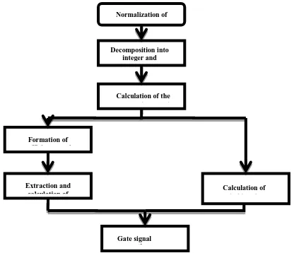
[image:2.595.63.271.264.443.2]Implementation of SVPWM strategy for controlling offers less harmonic distortion in the output voltages and currents. It gives flexibility in optimizing switching pattern design. A Low computational algorithm SVPWM for a multilevel multiphase system is proposed here [6]. The following flow chart summarizes the steps of the algorithm.
Fig. 2. Flow chart for the SVPWM implementation
1) Initially the normalized reference, Vr is obtained from the reference voltage vector Vdc using the expression.
2) Then decompose the normalized reference vector into the sum of its integer part, vi, and its fractional part, vf, by means of the equations
3) The next step is to calculate the permutation matrix P that sorts the vector vf in descending order in accordance with
4) Now rearrange the rows of the triangular matrix D in order to obtain the matrix D by means of
5) Further extract the displaced switching vectors, vdj, from the matrix D by taking into account the expression -
6) Now obtain the final switching vectors, vsj, by adding the integer part of the reference, vi, to the displaced switching vectors vdj according to equation.
7) Lastly the time corresponding to each switching vector is calculated from the components of the vector vf by means of the expression
As is evident, this is a generalized algorithm handling all the switching states, providing a sorted switching vector sequence which reduces the number of switching of the switches. This is hence capable of supporting any multi-level multiphase inverter system, enhancing the capability of the algorithm further. In this regard the algorithm is used for the proposed MLI topology here.
1.3 SIMULATIONRESULTS
[image:2.595.313.553.570.698.2]The software modeling of the system is carried out using MATLAB/SIMULINK. The Simulation parameters are shown in TABLE II –
TABLE II .Simulation Parameters
Parameter Value
Cell Voltage 4.5V
Control signal frequency 50Hz
Switching frequency 2KHz
Load
R load = 100 Ω L load = 100µH C load = 220µF
The proposed model was simulated for feeding passive loads - a resistive load and a resistive-inductive-capacitive load and the results are given below. Fig.3 shows the SVPWM pulses generated by the low computation SVPWM algorithm.
Normalization of the reference
voltage
Decomposition into integer and fractional parts
Calculation of the permutation matrix
Formation of coefficient matrix
Extraction and calculation of switching vectors
Calculation of switching time
© 2017, IRJET | Impact Factor value: 5.181 | ISO 9001:2008 Certified Journal | Page 375 Fig.4 and Fig.5 shows the MLI output waveform with R load
and R-L-C load respectively.
0 0.02 0.04 0.06 0.08 0.1
-0.5 0 0.5 1 1.5
Time in Sec
A m p li tu d e Gate Pulse
Fig.3. SVPWM pulses
0 0.01 0.02 0.03 0.04 0.05 0.06 0.07 0.08 0.09 0.1
-20 -10 0 10 20
Time in Sec
V a p h ( V )
MLI Output- Phase Voltage
Fig.4. Output waveform with R load
0 0.02 0.04 0.06 0.08 0.1 0.12 0.14
-20 -10 0 10 20
Time in Sec
V a p h ( V )
MLI Output- Phase Voltage
Fig.5. Output waveform with R-L-C load
The five level output is thus observed from the proposed model simulation. The pulses of the various switches can be observed to be different from each other due to the tracing of the levels as per the proposed switching states. Applying for an R-L-C load shows the approximately sinusoidal output waveform that is obtained. Filtering the output can provide near sinusoidal waveforms, promisingly better than Voltage Source Inverters with the voltage levels involved. Also this proves the effectiveness of the MLI topology as well,
compared to others for the same output voltage levels, attained with reduced number of switches though.
1.4 EXPERIMENTALSETUP
In addition to the simulation, a low power prototype of the proposed model was implemented. The proposed algorithm has been implemented using MATLAB interface with dSPACE DS1104. The obvious advantage of using hardware-in-loop simulations is that performance of systems for various operating conditions can be compared. Another feature of the dSPACE is the control desk which allows the graphical user interface, through the control desk the user can observe the response of the system, give command to the system through the interface [7-8]. The schematic of the experimental is shown in Fig.6
Fig.6. Hardware implementation schematic diagram
The hardware implementation of the proposed system can be divided into three parts:- Pulse generation circuit, Isolation circuit, and Power circuit.
The Pulse generation circuit consist mainly the MATLAB/Simulink model interfaced with dSPACE control card. The system implemented in MATLAB/Simulink, the model is converted to real time codes using a Real-Time Interface (RTI) of the control by the dSPACE DS1104 control card. The gate pulses generated by the model can be obtained at the Digital I/O pins of the dSPACE DS1104 I/O interface.
The pulses obtained from the interface are given to an Isolation circuit, employed to protect the pulse generation circuitry from the power circuit. A 12 pulse optocoupler isolator board is used as the isolation circuit. The isolated pulse outputs are given to the proposed MLI power Circuit.
The Power circuit consists of a 3 phase reduced MLI topology. Each phase has 5 switches with 2 of them bi-directional. Each phase of the power circuit needs 4 DC sources, which is provided by the Regulated DC Power Supply. The load used in this hardware prototype model is a resistive load and resistive-inductive-capacitive load.
© 2017, IRJET | Impact Factor value: 5.181 | ISO 9001:2008 Certified Journal | Page 376 Fig.7. Complete hardware setup
Fig.8. Hardware setup – Power circuit
Fig.9 shows the generated SVPWM pulses obtained after the isolation circuit, which are given to the switches. Fig.10 and Fig.11 presents the hardware output waveform with R load and R-L-C load respectively.
Fig.9. Hardware SVPWM pulses
Fig.10.Hardware output waveform with Resistive load
Fig.11. Hardware output waveform with Resistive-Capacitive load
The Hardware results can be observed thus to verify and validate the Simulation results. The output waveforms of both R and R-L-C loads are observed to be almost same in the simulation and hardware setup. The proposed system was thus successfully implemented as a prototype and its effectiveness was clearly observed.
2. CONCLUSIONS
The paper implemented satisfactorily a simplified low computational SVPWM algorithm for a reduced switch MLI topology. The observed results from both the simulation and the hardware implementation confirmed the successful Regulated
DC power
supply Power circuit
dSPACE
DC power supply
Isolation circuit
© 2017, IRJET | Impact Factor value: 5.181 | ISO 9001:2008 Certified Journal | Page 377 working of the proposed system of both the SVPWM algorithm
as well as the reduced switch MLI topology.
This proves the effectiveness of the simplified SVPWM algorithm generally a daunting issue for digital processors and also validates the improvement of the MLI topology. The results of the implemented prototype system hence promise improved and efficient performance in the high power system as well. This is especially useful for a drive system for which the quality of source voltage and performance is of major concern.
REFERENCES
[1] Drazen Dujic, Martin Jones, Emil Levi, “A space vector PWM scheme for multi frequency output voltage generation with multiphase voltage-source inverter”, IEEE Trans. Electronics, Vol.55 no.5. may2008
[2] C.Bharatiraja, Dr S. Jeevananthan, R. Latha, Dr S. S. Dash, “A Space vector pulse width modulation approach for DC link voltage balancing in diode clamped multilevel inverter”, Science direct AASRI Procedia 3- 2012,133-140
[3] Jesmin. F. Khan, Sharif M. A Bhuiyan, Kazi. M. Rahman, Gregory. V. Murphy, “Space vector PWM for a two phase VSI”, Science direct, Electrical power and energy system, 51 (2013) 265-277.
[4] Shieheng Zheng, Taotao Cui, Mu-Tian Cheng, Long Chen, “Research on variable frequency with three level topology and SVPWM control”, IEEE conference paper June 2012,978-1-4577-2088-8/11
[5] Thomas Nathenas, Heorgios Adamidis, “A new approach for SVPWM of a three- level inverter induction motor fed- neutral point balancing algorithm”, Science direct , 2012
[6] Zixin Li, Ping Wang, Haibin Zhu, Yaohua Li, “A New Simplified and space vector PWM Method for N-level Inverters”, IEEE Trans. Electronics, 2008, 978-1-4244-1718-6/08.
[7] Renukadevi. G; Rajambal. K., "Field programmable gate array implementation of space-vector pulse-width modulation technique for five-phase voltage source inverter," Power Electronics, IET , vol.7, no.2, pp.376,389, February 2014