Area and Timing Analysis of Different PSU’S in P-Match
Algorithm for Data Compression in Cache Memories
Nisha Angeline. M
Assistant Professor (Sr.Gr.),Department of ECE,
Velalar College of Engineering and Technology Erode, Tamilnadu
Manikandan.S.K
Assistant Professor (Sr.Gr.),Department of EEE,
Velalar College of Engineering and Technology Erode, Tamilnadu
Shree Subhatra.K
PG Student, Department of ECE,Velalar College of Engineering and Technology Erode, Tamilnadu
S.Valarmathy, PhD.
Professor and Head,Department of ECE,
Bannari Amman College of Technology, Sathyamangalam,Tamilnadu.
ABSTRACT
Microprocessors speeds have been increasing faster than the speed of off-chip memory. In a multi-processor system, if the processor number is increased, then the access time of the memory is also high. Thus a ‘wall’ is raised between processor number and memory access time. When compared with on chip cache, to access the data, off-chip cache takes one order of magnitude more time. Off chip cache also takes two orders of magnitude more time for executing an instruction, than on chip cache. Care should be taken in cache compression, to increase the processor speed but it should not contradict with the increase in the total chip’s power consumption. The compression is based on pattern coding and dictionary based matching and if the pattern matches, the code is chosen. Otherwise the dictionary matching is done. The compressor is composed of Pattern matching and Priority Unit. In this paper three different architectures for the priority selection unit is proposed and their area and timing analysis is done.
General Terms
Data Compression, Frequent Patterns, Performance analysis, Counters, Comparators, Adders.
Keywords
Cellular Automata (CA), Dictionary Matching (DM), Pattern matching (PM), Priority Selection Unit (PSU).
1.
INTRODUCTION
Memory latencies have long been a performance bottleneck in modern computers. In fact, with each and every advancement in technology, microprocessor execution rates outpace improvements in main memory speeds. Memory speeds are thus having increasing impact on overall processor performance. The rift between processor and memory speeds is alleviated primarily by using caches. Today’s microprocessors have on-chip cache hierarchies incorporating multiple megabytes of storage. Increasing the size of data in the on-chip caches can greatly increase processor performance. However, the amount of data storage in the on-chip cannot be increased without bound. In built caches almost consume most of the die area in high performance microprocessors. The fabrication costs of larger die are high,
and ultimately depend on semiconductor manufacturing technology. Practical cache sizes are constrained by the increased Memory bandwidth which is also a scarce resource in high-performance systems. Several researches use hardware based compression to increase effective memory size, reduce memory address and bandwidth and increase effective cache size.
The main objective of this paper is to increase the communicative capacity of the on-chip cache without degrading the performance issues. The ongoing move to chip-level multiprocessors (CMPs) is further increasing the problem; when the number of processors is increased, more accesses to memory occurs. This results in the reduced performance of the processor-memory bus which is not in pace. This problem is solved by techniques that reduce off-chip communication without degrading the performance. Data compression in memories is one such technique that helps to keep the pace of the bus. Data compression presents several challenges. The first one is increase in cache hit latency, which will favor in reduced cache miss rates. So this enhances extremely fast, data decompression and compression. Then secondly for reliable transmission the hardware should occupy little area compared to the corresponding decrease in the physical size of the cache, and care should be taken not to increase the total chip power consumption. Finally, cache compression should not increase power consumption substantially. The above requirements prevent the use of high-overhead compression algorithms .A faster and lower-overhead technique is required. Section II explains the related work regarding the data compression in Microprocessor Cache Memory. Section III explains the proposed work.
2. RELATED WORKS
2.1 Frequent Pattern Compression
is used for patterns like runs of zeros since they are very frequent. The main idea behind FPC is that we want to get most of the benefits of dictionary-based schemes, while keeping the per-line overhead at a minimum. The FPC compresses on a cache line basis. Each cache line is divided into 32-bit words (e.g., 16 words for a 64-byte line).These patterns are: a zero run (one or more all-zero words) and a one run(one or more all-one words), 4-bit sign-extended (including one-word zero runs), one byte sign-extended, one half words sign-extended, one half word padded with a zero half word, two byte sign-extended half words, and word consisting of repeated bytes (e.g. “0x20202020”, or similar patterns that can be used for data initialization). The input patterns are selected based on their high frequency in many of our integer and commercial benchmarks. A word that doesn’t belong to any of these categories is stored in its original 32-bit format.
The main idea behind compressing cache lines at L2 level in frequent pattern compression technique is to store common word patterns in a compressed format. Patterns are identified by a 3-bit prefix. The main advantage of this method is the decompression overhead, which helps to maintain cache lines in predetermined sizes. The drawback of this method is that there is no register-transfer-level hardware implementation or FPGA implementation of FPC, and therefore its exact performance, power consumption, and area overheads are unknown.
2.2 Restrictive Compression Technique
With the CMOS scaling trends and slow scaling of wires as compared to the transistors, the cache access latencies will increase in the upcoming microprocessor generations. To prevent the increasing latencies from affecting the cache throughput, the L1 caches are small-sized and their accesses are pipelined. Small-sized L1 data caches can result in significant performance degradation due to increased miss rates. Compression techniques can be used to boost the L1 data cache capacity. However, these compression techniques cannot alter the byte-offset of the memory reference, to avoid any increase in the cache access latency. Restrictive cache compression techniques [8] does not require updates to the byte-offset, and hence result in minimal, if any, cache access latency impact is present. The basic technique AWN (all words narrow) compresses a cache block only if all the words are of minute size. The compressed cache blocks are then combined together in a single physical cache block. The AWN technique requires minimal additional storage in the cache and results in a 20% increase in the cache capacity.
The AWN technique is extended by giving some supplementary space for the upper half-word AHS (additional half word space) of a few normal-sized words in a cache block, with an aim to convert them into narrow blocks. Further the AHS technique is extended to AAHS (adaptive AHS) so that the number of upper half-words in a cache block can adapt depending on the need. AHS and AAHS techniques increase the cache capacity by about 50%, while incurring a 38% increase in the storage space required, compared to a conventional cache. On the other hand, these techniques still do not impact the cache access latency. To reduce the extra tag requirements (which is inevitable with any cache compression technique), this method focuses to reduce the number of additional tag bits provided for the additional cache blocks to be placed in a physical cache block, sinking the overhead of the AHS techniques to about 30%.
The byte-offset value of every word present in the block is greatly depended on the size of the words present before it in the cache. This will result in recalculating the byte-offset to read a word from the block. Therefore, it is crucial that any compression technique that is used in the L1 caches will not have the need of updating the byte-offset. Such compression techniques can be called as restrictive compression techniques. The drawback of this technique is that it cannot alter the byte-offset of the memory reference, to avoid any increase in the cache access latency.
2.3 Indirect Index Cache with Compression
Indirect index cache [5] allocates variable amount of storage to different blocks, depending on their compressibility. The Indirect Index Cache with Compression is based on the IIC. The basic IIC consists of a data array containing the cache blocks and a tag store which contains the tags for these blocks. Every tag of IIC entry holds a pointer to the data block with which it is currently associated. This indirection provides the ability to implement a fully associative cache.
Replacements in the IIC are managed by a software algorithm running on an embedded controller or as a thread on the main CPU. The main algorithm, called Generational Replacement (GEN), maintains prioritized pools (queues) of blocks; updated periodically while referenced blocks are moved to higher priority pools and unreferenced blocks are moved to lower priority pools. At first replacements are done by choosing the un-referenced blocks from the lowest priority pool. Incase of reaching the highest priority pool, a block must be referenced regularly over an extended period of time; once there. After doing this it must remain unreferenced for a similarly long period to return to the lowest priority pool. This algorithm thus combines reference regency and frequency information with a hysteresis effect, when dealing with block reference bits and periodic data structure updates. To ensure that adequate replacement candidates are available to deal with bursts of misses, the algorithm can identify multiple candidates per invocation and maintain a small pool of replacement blocks. This small pool of replacement blocks are used by hardware to handle incoming responses, while GEN algorithm is used in the background to keep this pool at a predetermined level. The IIC was originally designed to utilize large on-chip caches to achieve better performance over traditional LRU caches. The main drawback of this technique is that one cannot reliably determine whether the architectural schemes are beneficial without, a cache compression algorithm and hardware implementation, while they are designed and evaluated for effective system-wide compression ratio, and other performance issues like hardware overheads, and interaction with other portions of the cache compression system.
2.4 Selective Compression Technique
high performance is achieved by increasing the compression over head, with minimum loss in the retrieval of original data.
It is not easy to suggest that this architecture is beneficial without a proper compression algorithm or its hardware implementation, even though it has improved parameters like over all compression ratio and performance metrics like compression overhead and speed of responding to other modules of the system, which is a the demerit of this technique.
2.5 X-Match Compression Algorithm
X-Match is a dictionary-based compression algorithm that has been successfully implemented on the FPGA kit [7]. It results in relates 32-bit words using a content addressable memory that results in partial matching with dictionary entries and outputs of encoded data with variable size that depends on the type of match. To enhance the coding efficiency, it also uses a move-to-front coding approach and smaller indexes are represented with fewer bits. Even though it is appropriate for compressing main memory, such hardware typically has a very large block size (1 KB for MXT and up to 32 KB for X-Match), which is inappropriate for the compression of cache lines. It is well known that for X-Match and two other algorithms of Lempel-Ziv algorithm, i.e., LZ1 and LZ2, the compression ratio for the data in memory deteriorates with smaller block size [5].For instance, the increased compression ratio for LZ1 and X-Match algorithm is nearly 11% and 3% with the reduction in block size from 1KBto 256 B. It is studied that the increase in compression ratio could be larger if the block size decreases from 256 B to 64 B. In addition, such hardware has to challenge its use in cache compression because of performance metrics like area and power consumption costs. For instance, if the MXT hardware was scaled to a 65 nm fabrication process and integrated within a 1 GHz processor, the decompression latency would be 16 processor cycles, almost two times higher than the normal L2 cache hit latency.
2.6 C-Pack Compression Algorithm
C-Pack targets on-chip cache compression. Even when used on small cache lines it gives a good compression ratio. The performance metrics like area and power consumption overheads are low such that it can suit a practical purpose. This idea is in contrast with other schemes such as X-match where a complicated hardware is needed to achieve an equivalent effective system-wide compression ratio. The early work in cache compression does not tolerably evaluate the overheads resulting from the assumed cache compression algorithms. C-Pack is almost two times faster than the best existing hardware implementations potentially suitable for cache compression. For other methods like FPC, to match this performance, it would require at least 8* the area of C-Pack. The main drawback of this technique is that Compression is not performed in all the cases. When the total number of compressed bits exceeds the uncompressed line size, the content of the backup buffer is selected. Here the backup buffer has the actual 64 bit uncompressed word. Compression is made in the ratio of 2:1.Due to its efficiency it cannot be expanded. Frequently used instructions are compressed and stored in FIFO [3]. When that particular instruction leaves the dictionary it re-enters the dictionary in uncompressed form and it has to be again compressed. Hence the memory is not properly used.
3. PROPOSED ARCHITECTURES
3.1 Compression Architecture 2:1 Ratio
[image:3.595.314.542.160.552.2]In the proposed 2:1 architecture shown in Figure.2 is having two pipeline stages. The compression is mainly done as shown in Table1.
Table .1 Pattern encodings for the proposed method
Figure 1 Compression example
3.1.1 Pipeline stage1:
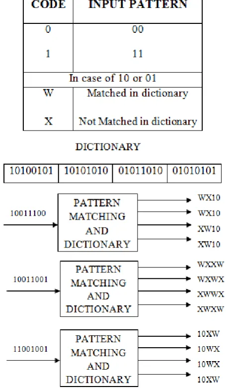
The first pipeline stage performs pattern and dictionary matching on eight uncompressed words in parallel. Each of the eight 8 bits will match with the instruction in dictionary and produces four 4 bit words. After dictionary matching they are concatenated .The output W1, W2, W3 and W4 each has 32 bit and it is fed to the next pipeline stage. The pattern and dictionary matching is done as shown Figure 1.
3.1.2 Pipeline stage2:
The second pipeline stage performs the selection of word from W1, W2, W3, and W4 depending on the priority. The
Figure.2. Compression architecture (2:1 compression ratio)
Figure.3 Compressor architecture (4:1 compression ratio)
one’s, Second priority will be give to all zero’s, third priority will be given to the combination of zero’s and one’s, next priority will be given to matched bytes and the least priority will be given to unmatched bytes. This is possible only by counting the number of zero’s, one’s, matched bytes and unmatched bytes. Counter 0, counter 1 and counter W counts the number of zero’s, one’s and the matched bytes. The counting does not include the number of unmatched bytes. Later they are selected based on their priority. This work is performed by the comparators. If both the inputs to the comparator have same numbers of zeros, ones and matched bytes then the first input to the comparator will be the output of the comparator. The output of the selection unit will be the compressed 32 bit word. Thus a 64 bit word is compressed to 32 bit word with a compression ratio of 2:1.For example when the input pattern is 11001001 and the dictionary patterns are 11000110, 11010010, 11100000 and 10101010 then the output patterns will be 10xx, 10xx, 10xx and 10wx.If the
input pattern given is
10100101111000010110000101100001111
1000101110001011010011100001 the output pattern obtained
after compression is
1x0w1100w100w10011w0w1w0w1x01w0x which is compressed in the ratio of 2:1.
3.2 Compression Architecture 4:1 Ratio
The proposed architecture can be enhanced by implementing the compression with the compression ratio of 4:1. Figure.3 illustrates the hardware compression process. The compressor is decomposed into two pipeline stages.
3.2.1 Pipeline stage1:
The first pipeline stage performs pattern and dictionary matching on four uncompressed words in parallel. Each of the four 16 bits will match with the instruction in dictionary and produces four 4 bit words. After dictionary matching they are concatenated .The output W1, W2, W3 and W4 each has 16 bit and it is fed to the next pipeline stage.
3.2.2 Pipeline stage 2:
The second pipeline stage performs the selection of one word from W1, W2, W3, and W4 depending on the priority. The first priority is give to all one’s, Second priority will be give to all zero’s, third priority will be given to the combination of zero’s and one’s, next priority will be given to matched bytes and the least priority will be given to unmatched bytes. This is possible only by counting the number of zero’s, one’s, matched bytes and unmatched bytes. Counter 0, counter 1 and counter W counts the number of zero’s, one’s and the matched bytes. The counting does not include the number of unmatched bytes. Later they are selected based on their priority. This work is performed by the comparators. If both the inputs to the comparator have same numbers of zeros, ones and matched bytes then the first input to the comparator will be the output of the comparator. The output of the selection unit will be the compressed 16 bit word. Thus a 64 bit word is compressed to 16 bit word with a compression ratio of 4:1.For example when the input pattern is 11001001 and the dictionary patterns are 11000110, 11010010, 11100000 and 10101010 then the output patterns will be 10xx, 10xx, 10xx and 10wx.If the input pattern given is 10100101111000010110000101100001111
after compression is 1x0w1100w100w10011w0w1w0w1x01w0x which is compressed in the ratio of 4:1.
3.3 Priority Selection Unit (PSU)
In this compressor architecture, Priority selection unit plays an important role. It selects the maximum matched word from the pattern generated by the Pattern matching unit. Three different structures are proposed and their corresponding timing and area analysis is done using Xilinx Spartan 3E FPGA Kit. Four inputs are given to each PSU. Out of these four words one is chosen as the output. This output is the one that has maximum number of zeros, ones, and most matched bytes.
3.3.1 Priority selection unit 1(PSU 1):
The first structure of the priority selection unit has three counters for counter 0, counter 1, counter w (to count number of zeros, ones and matched bytes). Eight two input adders sum the outputs of the counters. The greatest value of the sum is selected with the help of three comparators. Finally the word corresponding to the greatest value of the sum is selected from the selector as in Figure.4
Figure.4 Priority selection unit 1 architecture.
3.3.2 Priority selection unit 2(PSU 2):
Figure.5 Priority selection unit 2 architecture
The second structure of PSU helps in reducing the adder complexity, thereby reducing the counter complexity, as shown in Figure.5. Since the number of zeros and ones remain the same for all the four input words they are counted only once. The eight adders in the above structure, is reduced to five adders. The output of counter 0 and counter 1 is summed up in the first adder. This sum along with the four outputs of the counter w (counter of matched words) contribute as the inputs to the next four adders. Due to this, area occupied will be less compared to the previous work.
3.3.3 Priority selection unit 3(PSU 3):
When analyzing the above three structures we can come to a conclusion that the output of counter 0 and counter 1 is the same for all the four words. Hence neglecting both the counters will not affect the selection of the most matched word, as the priority selection mainly depends on the counter w. The architecture for this unit is shown in Figure.6
Figure.6 Priority selection unit 3 architecture
4. RESULTS & DISCUSSIONS
4.1 Simulation Results
We simulated our design using Model sim version 10 and obtained three simulation results for each priority selection unit with four bit input word. Figure.7 has many internal signals and shows the output for the architecture of PSU1, while Figure.8 is the output for the architecture of PSU2. The PSU3 output is shown in Figure.9
Figure.7 Priority selection unit 1 output
Figure.9 Priority selection unit 3 output
4.2 Comparison Tables
4.2.1 Compression ratio comparison
We compared our algorithm to several other hardware compression designs namely C-pack, FPC, X-match, and MXT, that may be considered for cache compression.
Table.2 Compression Ratio comparison
The Table.2 indicates the compression ratio which varies from algorithm to algorithm. P-Match is being the best and MXT being the worst.
4.2.2 Timing analysis
The advanced HDL synthesis showing the decreasing CPU time for the PSU’s is in Table 3. The PSU1 has the largest simulation time between 2.57ns and 2.65 ns while the PSU3 has the least simulation time between 2.33ns and 2.42ns.
4.2.3 Area analysis
The decreasing simulation time is due to the reduction in hardware complexity, which can be understood from Table 4. The PSU3 does not have adders and occupies the least area. The PSU2 has 15 adders less when compared to the PSU1 structure.
5. CONCLUSIONS
This paper has proposed and evaluated an algorithm: P-match for cache compression that honors the special constraints this application imposes. The algorithm is based on pattern coding and partial dictionary coding. Then the priority selection unit chooses the most matched word. Four different PSU structures have been proposed and they are compared. Though the proposed hardware implementation mainly targets online cache compression, it can also be used in other high-performance lossless data compression applications with few or no modifications.
Table.3 Timing analysis comparison
PARAMETER PSU1(ns) PSU2(ns) PSU3(ns)
CPU Time 2.57/2.65 2.49/2.58 2.33/2.42
Total real time to MAP completion 2 0 0
Total REAL time to PLACER completion
2 0 0
Total REAL time to ROUTER completion
2 1 1
Total REAL time to PAR (PLACE AND ROUTE)completion
3 1 1
Table.4 Timing analysis comparison
PARAMETERS PSU1 PSU2 PSU3
1 bit adder carry out 8 4 -
2 bit adder 8 4 -
2 bit adder carry out 8 4 -
32 bit adder 8 5 -
TOTAL NO. OF ADDERS 32 17 -
32 bit comparator(equal) 3 3 3
32 bit comparator(less) 3 3 3
TOTAL NO. OF
COMPARATORS
6 6 6
6. SCOPE FOR FURTHER RESEARCH
The decompression of the proposed 2:1 architecture will be a lossless method where as the decompression of the proposed 4:1 architecture is somewhat tedious process. Even though it can be made easy, the decompression of the proposed 2:1 and 4:1 architecture is my future work which is not stated in this paper. My only objective now is to design a compressor architecture which compresses the input pattern without any
7. ACKNOWLEGMENTS
The authors acknowledge the contributions of the students, faculty, Velalar College of Engineering and Technology, the Research Center and would like to particularly thank Bannari Amman Institute of Technology, Sathyamangalam for help in the design of test circuitry, and for tools support. The authors also thank the anonymous reviewers for their thoughtful comments that helped improve this paper. The authors would like to thank the anonymous reviewers for their constructive critique from which this paper greatly benefited.
8. REFERENCES
[1] M.Nisha Angeline , Prof.S.Valarmathy , S.K.Manikandan , Prof. C.Palanisamy, ‘‘VLSI Design Of Cache Compression in Micro Processor using Pattern Matching Technique’’ in IOSR journal of Electronics and Communication Engineering, Vol 1,Issue 6, July-August 2012.
[2] A.Deepa, M.Nisha Angeline and C.N. Marimuthu, “ P-Match: A Microprocessor Cache Compresion Algorithm”, 2nd
International Conference on Intelligent Information Systems and Management (IISM’11), July 14- 16, P.No.98, 2011.
[3] Xi Chen, Lei Yang, Robert P. Dick “C-Pack: A High – performance Microprocessor Cache Compression Algorithm.”. IEEE transactions on very large scale integration (VLSI) systems, Vol. 18, No. 8, August 2010.
[4] A.Alameldeen and D. A. Wood, (2004) “Frequent pattern compression: A significance-based compression scheme for 12 caches,” Dept. Comp. Scie. , Univ. Wisconsin-Madison, Tech. Rep. 1500.
[5] E.G.Hallnor and S.K.Reinhardt, (2004) “A compressed memory hierarchy using an indirect index cache,” in Proc. Workshop Memory Performance Issues, pp. 9–15.
[6] J.-S. Lee et al., (1999) “Design and evaluation of a selective compressed memory system,” in Proc. Int. Conf. Computer Design, pp. 1
[7] J. L. Nunez and S. Jones, “Gbit/s lossless data compression hardware,” IEEE Trans. Very Large Scale Integr. (VLSI) Syst., vol. 11, no. 3, pp.499–510, Jun. 2003
[8] P. Pujara and A. Aggarwal, (2005) “Restrictive compression techniques to increase level 1 cache capacity,” in Proc. Int. Conf. Computer Design, pp. 327– 333.
AUTHOR’S PROFILE
Nisha Angeline. M received her B.E degree in Electronics and Instrumentation Engineering from the Indian Engineering College, Thirunelveli District in 2003 and M.E –VLSI Design in Kongu Engineering College, Perundurai in the year 2006.
She is working as a Professor (Sr.Gr) in the department of ECE, Velalar College of Engineering and Technology, Erode. Currently she is doing Ph.D under Anna University in the area of VLSI Design. She has published two papers in International Journals and presented five papers in National and International Conferences. Her areas of interest are Digital Electronics, VLSI Architecture, and VLSI Signal Processing.
Shree Subhatra.K received her B.E degree in Electronics and Communication Engineering from Anna University, Coimbatore, 2011. She is currently pursuing Master of Engineering in VLSI Design in Velalar College of Engineering and Technology under Anna University, Chennai. Her areas of interest in research are VLSI Signal Processing, VLSI architectures.
Manikandan.S.K has received B.E degree in Electronics and Communication Engineering from Annai Mathammal Sheela Engineering College, Namakkal District, 2003 and M.E – Embedded Systems from Sasthra University, Tanjore District in the year 2006. He is working as a Professor (Sr.Gr.) in the department of EEE, Velalar College of Engineering and Technology, Erode. Currently he is doing Ph.D under Anna University in the area of VLSI Design. He has published two papers in International Journals and presented five papers in National and International Conferences. His areas of interest are Microprocessor and Microcontroller, ARM Processor, VLSI architectures.