Acknowledgements
In 1997, I began my graduate study at Hitotsubashi University. In 2001, I attended Northwestern University, and three years later, I transferred to the London School of Economics. This Ph.D. thesis is the result of my studies at these distinguished universities. I would like to express my gratitude to all who enabled me to complete this thesis.
I am extremely grateful to my supervisors, Professor Janet Hunter and Dr. Tom Nicholas, whose help, stimulating suggestions, and encouragement helped me throughout the research and writing of this thesis. Professor Hunter was always supportive and constrictive. Her understanding, encouragement, and guidance have provided an important basis for the present thesis. Since Dr. Nicholas left the London School of Economics and moved to Harvard Business School in 2005, I lost an important mentor. However, he always read drafts and provided constructive comments.
At Hitotsubashi University, I became interested in Innovation and Knowledge Creation, which are the key issues of my thesis. I would like to express my warmest and sincere thanks to Professor Seiichiro Yonekura. He gave me the opportunity to visit Boston and meet the late Alfred Chandler Jr. in the summer of 1997. Without this visit and his guidance, I would have not decided to study abroad. His concept-creating orientation, inspiring work, and fanatical inclination to tennis and personal friendship encouraged me and changed my career. Professor Yoshitaka Suzuki recommended LSE for me. I warmly thank him for his valuable advice and help. I would like to thank Professor Tsuyoshi Numagami and Dr Toshihiko Kato as well. Professor Numagami’s classes and work are always in my mind. His ideals and concepts have had a remarkable influence on my entire graduate studies. Since Dr Kato was visiting City University from 2004 to 2005, I was able to consult with him several times in London. His encouragement and insightful comments on my thesis were valuable. I would like to thank Professors, Ikujiro Nonaka, Hiroyuki Itami, and Akira Takeishi who were on the faculty of Hitotsubashi University. I would also like to thank the graduate students while I was at Hitotsubashi: Minoru Shimamoto, Kazuhisa Kawai, Kenji Inayama, Daiji Fujii, Kunio Miyazaki, and Takashi Hirao. The continuous conversations with many Hitotsubashi scholars has kept my mind turning and my reading list very long.
At Northwestern University, Professor Laura Hein and Dr. Peter Murmann gave me tremendous support. Professor Joel Mokyr gave me advice when I planned to transfer to LSE.
Duran, Calros Stantiago-Caballero, and Ashishi Velkaer for giving constructive comments and welcome support. I would like to thank Makoto Kasuya, who was a visiting scholar at LSE from the University of Tokyo, for his constructive and insightful comments on my research.
I would like to thank the late Jurō Hashimoto. At a social gathering after an academic conference, he inspired me with kind words. His written scholarship and words of encouragement have been an endless source of support. And I would like to thank all corporate managers, engineers, and government officials who kindly took time for my interviews. I was impressed to witness their passion and excitement for their expertise in the development of laser technology.
On a more personal level, I want to thank my parents, Akira and Kyoko. Without their support, I could have not finished this thesis. Yet none is greater than the one I owe to Yasuko Shimizu, my wife. Her encouragement and assistance never wavered.
Abstract
Knowledge plays an important role in economic growth. The role of technological knowledge significantly increased after the Industrial Revolution. Firms internalised technological knowledge in their R&D laboratories and placed knowledge creation in a central position in their business strategies. Both the stock and flow of technological knowledge and the tight interaction among science and engineering became indispensable to the competitive advantage of industry, as well as modern economic growth.
Directing its attention to knowledge creation and spillover, this thesis scrutinises the development of semiconductor lasers from 1960 to 1990. The semiconductor laser became one of the most important developments in the optoelectronics industry underlying the drastic changes that took place during the last half of the twentieth century in information technology, and it has become the most widely used laser since the 1980s.
Reviewing the optoelectronics industry in the U.S. and Japan, the Japan Technology Evaluation Center (JTEC) found that “Japan clearly led in consumer optoelectronics, that both countries were competitive in communications and networks, and that the United States held a clear lead in custom optoelectronics.” “Japan’s lead in high-volume consumer optoelectronics and related technologies gave it a dominant share of the overall global optoelectronics market.” This thesis explores how the patterns of comparative advantages emerged, which were indicated by the JTEC report. How did Japanese firms gain technological competitiveness in high volume product markets? How did the U.S. firms come to be competitive in niche markets?
Table of Contents
1. Introduction ...9
1.1. Knowledge, Knowledge Spillover and Technological Change ...11
1.2. Semiconductor Laser ...25
1.3. Epitaxy Technology ...38
1.4. Approach and Contribution...42
2. Literature Review: Technological Development in Post-war Japan ...65
2.1. Economic Growth and Two Exogenous Shocks...66
2.2. Four Perspectives on Technological Change and Economic Growth...72
2.3. Previous Studies and Research Questions ...90
3. Human Capital and Research Networks ...93
3.1. The Beginning of Semiconductor Laser Research ...95
3.2. Accumulation of Human Capital ...101
3.3 Collaborative Research and Networks...106
3.4. Conclusion ...117
4. Semiconductor Laser Research Consortium: the OMCS Project ...119
4.1 Previous Research and Approach ...121
4.2 Optoelectronics Measurement and Control System Project ...126
4.3. Underinvestment of the Participating Firms...135
4.4. Competition Enhancement Effect...142
4.5. Conclusion ...148
5. Competition, Knowledge Spillover, and Innovation...151
5.1. Invention of the Semiconductor Laser and LPE...153
5.2. New Market and Technological Change...159
5.3. Economic Context and Vertical Integration...173
5.4. Competition and Knowledge Spillover ...186
5.5. Conclusion ...204
6. Conclusions and Implications ...207
6.1. Summary of the Arguments ...208
6.2. Contribution...211
6.3. Discussions and Implications ...213
Appendix I: Number of Doctorates Awarded in Semiconductor Laser in the World ...230
Appendix II: Institutions and Co-Publications ...234
Appendix III: List of Interviewees ...239
Appendix IV: Consortium Expenditure in U.S. Dollars ...243
Appendix V: Top Fifty Engineers and their Affiliations...244
Appendix VI: Laser and Semiconductor Laser...247
List of Tables
Table 1-1: R&D Intensity in Japan ...27
Table 1-2: Optoelectronics Production and Presence in GDP (Billion Yen) ...28
Table 1-3: Laser Sales in Japan (Million Yen)...29
Table 1-4: Competitive Advantage of the Nations in Technical Field...31
Table 1-5: Top Twenty Firms in Japan...34
Table 1-6: Two Main Markets of Semiconductor Lasers (Million yen) ...36
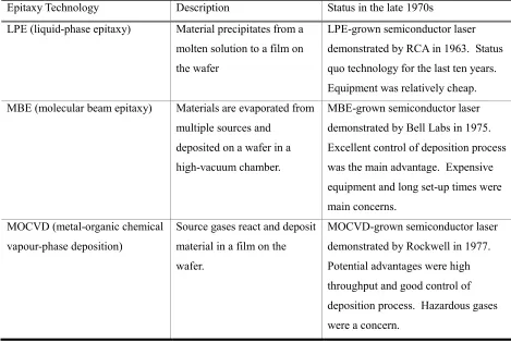
Table 1-7: Three Epitaxy Technologies: LPE, MBE, and MOCVD...41
Table 3-1: Top 10 Institutions in the Cummulative Number of Doctoral Degrees Granted 1965-1985 ...105
Table 3-2: Number of Articles and Co-Publications 1962-1985 ...108
Table 3-3: Number of Organisations and Inter-Organisational Co-Publications 1962-1985 ...109
Table 3-4: Scale and Scope of Research Networks ...115
Table 4-1: OMCS and Other Large Scale Projects 1962-1992...128
Table 4-2: Participating Firms ...129
Table 4-3: R&D Investment and Number of Firms in 1990 ...131
Table 4-4: Sub Research Groups in Joint Research Laboratory ...133
Table 4-5: Semiconductor Laser-Related Product Markets of Participants...137
Table 4-6: Patent Citation: OMCS and Participating Firms’ Private R&D ...139
Table 5-1: U.S. Firms in Semiconductor Laser R&D 1970-1975 ...156
Table 5-2: Japanese Firms in Semiconductor Laser R&D 1970-1975 ...156
Table 5-3: Changes in World Market Share in 1960-1986 ...177
Table 5-4: Semiconductor Laser and Final Products of the U.S. Firms 1984, 1987 and 1991...181
Table 5-5: Semiconductor Laser and Final Products of Japanese Firms 1984, 1987 and 1991...183
Table 5-6: Patent Citation by Japanese Firms...191
Table 5-7: Example of Venture Business in Semiconductor Lasers ...197
Table 5-8: Mobility of Top Fifty Engineers ...200
Table 5-9: U.S. Star Engineers...200
Table 5-10: Japanese Star Engineers ...202
List of Figures
Figure 1-1: Semiconductor Laser ...25
Figure 1-2: World Patents and Japan Patents (Accumulative)...32
Figure 1-3: Epitaxy Process...39
Figure 1-4: Separation Process ...39
Figure 1-5: Packaging Process...40
Figure 1-6: Timing of R&D and Profit ...48
Figure 2-1: Technological Innovation and Production Frontier ...70
Figure 2-2: Dominant Design, Product Innovation, and Process Innovation ....75
Figure 3-1: Number of Semiconductor Laser Publications ...99
Figure 3-2: Accumulative Number of Doctoral Degrees...103
Figure 3-3: Accumulative Number of Doctoral Degrees Per Capita ...104
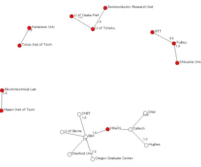
Figure 3-4: Direct and Indirect Connections ...110
Figure 3-5: The U.S. Collaborative Organisational Networks ... 111
Figure 3-6: Japanese Collaborative Organisational Networks ...113
Figure 3-7: Europe Collaborative Organisational Networks ...114
Figure 4-1: Cumulative Number of Patents in the Semiconductor Laser...144
Figure 5-1: LPE Technology...158
Figure 5-2: MBE Technology ...164
Figure 5-3: MOCVD Technology...165
Figure 5-4: The Number of Patents in LPE, MBE, and MOCVD...167
Figure 5-5: Technological Choice of U.S. Firms...169
Figure 5-6: Technological Choice of Japanese Firms...170
Abbreviations
Abbreviation Formal Name
AIST Agency of Industrial Science and Technology of Japan CALTECH California Institute of Technology
ETL Electrotechnical Laboratory (MITI’s Research Laboratory) GHQ General Head Quarter
He-Ne Helium-Neon
HP Hewlett-Packard Company IBM International Business Machines JAP Journal of Applied Physics JAPL Journal of Applied Physics Letters JTEC Japan Technology Evaluation Centre
KDD Kokusai Denshin Denwa (International Telegram and Telecommunication) LASER Light Amplification by Stimulated Emission
LPE Liquid Phase Epitaxy
MASER Microwave Amplification by Stimulated Emission
MBE Molecular Beam Epitaxy
MIT Massachusetts Institute of Technology MITI Ministry of International Trade and Industry MOCVD Metal-Organic Chemical Vapour-phase Deposition
NASA National Aeronautics and Space Administration NEC Nippon Electric Company, Ltd
NTT Nippon Telegraph and Telephone Corporation RCA Radio Corporation of America
OITDA Optoelectronics Industry and Technology Development Association OMCS Optoelectronics Measurement Control System
SCAP Supreme Commander for the Allied Powers
SEMATECH Semiconductor Manufacturing Technology Consortium
1.
Introduction
Following from Albert Einstein’s 1905 theoretical conception of the
photoelectric effect, an American physicist, Gordon Gould, invented Laser (Light
Amplification by Stimulated Emission of Radiation) in 1958. It was called “the
greatest invention of the century.”
A laser is an optical source that emits a narrow beam of coherent light. The
power in a continuous beam ranges from a fraction of a milliwatt to more than a
mega watt. The range of laser application is broad in scope ranging from
commercial uses to special military applications.
The semiconductor laser became one of the most important technologies
underlying the dramatic changes that took place during the last half of the 20th
century in information technology, and it has become the most widely used laser
since the 1980s. It is mainly used for information storage such as the compact disc
and digital videodisc system, which can store a 30-volume encyclopaedia set of
information on a disc and can access an arbitrary element of information in equal
time. It is also employed for fibre-optic communication, which permits digital data
transmission over long distances and at higher data rates than electronic
communication.
Reviewing the optoelectronics industry in the U.S. and Japan in 1996, the
Japan Technology Evaluation Center (JTEC) estimated that “Japan now dominates
some 90% of the world optoelectronics markets and can be expected to continue its
dominance for a number of years.”1 It also indicated, “Japan clearly led in consumer
optoelectronics, that both countries were competitive in communications and
networks, and that the United States held a clear lead in custom optoelectronics.”
“Japan’s lead in high-volume consumer optoelectronics and related technologies
1
gave it a dominant share of the overall global optoelectronics market.”2
Scrutinizing the development of semiconductor laser technology from 1960
to 1990, this thesis explores how the patterns of comparative advantages indicated
by the JTEC report emerged. How did Japanese firms gain technological
competitiveness in high volume product markets? How did the U.S. firms come to
be competitive in niche markets?
This chapter contains four sections. The first section aims to present key
issues of this study and to induce the research questions by overviewing the previous
theoretical literature about competition, knowledge spillover, and technological
change in technology-intensive industries. The second and third section introduces
semiconductor laser and its epitaxy technology, which is the most important
semiconductor laser technology. The last section presents this thesis’s approach to
these research questions. It introduces the research design, perspectives, and
measurement methodology. It also presents the sources and an outline of the
argument of the study.
2
1.1. Knowledge, Knowledge Spillover and Technological Change
3Technology and technological knowledge played an important role in
economic growth. The British Industrial Revolution (1760-1830) was the first event
of modern times in which technological changes reshaped society and accelerated
innovation. Indicating that the growth of the stock of knowledge played a important
role in modern economic growth, Kuznets incorporated knowledge in the framework
of economic analysis.4 He argued, “indeed, one might define modern economic
growth as the spread of a system of production, in the widest sense of the term,
based upon the increased application of science, that is an organized system of tested
knowledge.”5 However, Mokyr noted that Kuznets’s theory did not attract much
attention.6 One of the reasons was that economic historians found that the role of
scientific knowledge in the British Industrial Revolution was quite modest.7
The role of technological knowledge, however, significantly increased after
the Industrial Revolution.8 Pharmaceutical and chemical firms (e.g., Du Pont) were
probably the first to allocate an enormous amount of resources to R&D.9 Examining
three dominant technologies--the internal combustion engine, chemicals, and electric
power--in the U.S., Mowery and Rosenberg described how funding, institutional
3 The second chapter, Literature Review: Technological Development in Post-war Japan,
will more broadly review the previous studies of technological change in post-war Japan to show how this study aims to contribute to the broader line of previous arguments. This section focuses on the studies arguing the relationship between knowledge spillover and competition, which is the focus of this study.
4 Kuznets, Economic Growth and Structure. 5 Ibid, p.84.
6 Mokyr, "Innovation in an Historical Perspective: Tales of Technology and Evolution", p.
25.
7 On recent discussions on the role of scientific revolution in the British Industrial
Revolution, see Allen, "The British Industrial Revolution in Global Perspective: How Commerce Created the Industrial Revolution and Modern Economic Growth"; Khan and Sokoloff, "The Evolution of Useful Knowledge: Great Inventors, Science and Technology in British Economic Development, 1750-1930."
8
Mokyr, "Innovation in an Historical Perspective: Tales of Technology and Evolution."
9
settings (e.g., patent law), and R&D systems interacted to shape the path of
innovation.10 Examining the consumer electronics and computer industry, Chandler
et al. revealed that the firms internalised technological knowledge into their R&D
laboratories and placed knowledge creation in a central position in their business
strategies.11 It is generally accepted that both the stock and flow of technological
knowledge and the tight interaction among science and engineering became
indispensable to the competitive advantage of industry and firms, as well as modern
economic growth.12
Knowledge Spillover
Regarding knowledge, technology, and human capital as exogenous factors,
neo-classical economics used to view labour and capital as the only two factors of
production important for manufacturing. However, the new growth theory contends
that both knowledge and technology play significant roles in long-term economic
growth.13 New knowledge is a source of innovation and contributes to productivity
growth. Knowledge spillovers also play crucial roles in various economic contexts.
Much of the current literature in both economics and economic history agrees that
knowledge creation and spillover are important factors leading to economic growth.
Reviewing the previous literature, this section discusses the two standpoints on
competition and technological spillover, which induce the research questions.
Maintaining that technological knowledge is inherently a public good,
Kenneth Arrow focused on non-rivalness and non-excludability.14 First, an unlimited
10 Mowery and Rosenberg, Paths of Innovation: Technological Change in 20th-Century
America.
11 Chandler et al., Inventing the Electronic Century: The Epic Story of the Consumer
Electronics and Computer Industries.
12 Regarding the relationship between science and industry, see Rosenberg, "How
Exogenous Is Science?"
13 For example, Grossman and Helpman, Innovation and Growth in the Global Economy;
Grossman and Helpman, "Endogenous Innovation in the Theory of Growth"; Romer, "Increasing Returns and Long-Run Growth"; Romer, "Endogenous Technological Change."
14
number of agents can use the same technological knowledge at the same time.
Second, once a firm has publicly released technological knowledge, it is difficult for
the firm to keep other firms from using that knowledge. These characteristics of
technological knowledge play an important role in knowledge spillovers.
While no formal definition of knowledge spillovers exists, Griliches’s
definition has been most straightforward. He has defined knowledge spillovers as
“ideas borrowed by research teams of industry i from the research results of industry
j.”15 Following Griliches’s definition, this thesis defines technological knowledge
spillover as learning or knowledge externalities from another firm’s R&D.
Spillovers occur because new knowledge created by an organisation cannot
be kept perfectly secret in the organisation. Technological knowledge emerges in
numerous ways. Technological knowledge leaks out through patents, academic
papers, and academic presentations.16 It is also transferred when knowledge-bearing
employees change firms. Additionally, knowledge spillovers arise through informal
personal relationships.
Knowledge spillovers play significant roles in various economic and
business contexts. Following Schumpeter and Solow, recent economic growth
literature maintains the importance of knowledge spillovers in sustainable economic
growth. For instance, assuming that knowledge input in production increases
marginal productivity, Romer presented a model of long-run economic growth based
on the new growth theory.17 Developing economic growth models, Grossman and
Helpman proposed that technology spillovers, which bring about increasing returns,
are the engine of endogenous economic growth.18 In their model, the innovative
technological information, see Arrow, "Economic Welfare and the Allocation of Resources for Invention."
15 Griliches, "The Search for R&D Spillovers", p.13.
16 Appleyard has suggested that there are many different ways of knowledge sharing and
technological knowledge leaking. Appleyard, "How Does Knowledge Flow? Interfirm Patterns in the Semiconductor Industry", pp.139-140.
17 Romer, "Increasing Returns and Long-Run Growth"; Romer, "Endogenous Technological
Change."
18
activities of firms not only lead to the introduction of new products and the
improvement of product quality, but they also contribute to a general stock of
knowledge on which subsequent innovators can build. This knowledge base grows
over time, allowing innovation without the continual increase of R&D resources.
Taking the discussion of technological knowledge spillover one step down from the
national economy to corporate R&D, Griliches argued that technological spillover is
a source of increasing returns in R&D and enhances technological development.19
Bernstein and Nadiri calculated social and private rates of return and estimated the
effects of R&D spillovers.20 Their estimation found that R&D spillovers brought
important positive returns to both society and a firm and that the social return
exceeded the private return, even though there is significant variation across
industries in the differential between the social and private rate of return.
New knowledge in an R&D project affects the productivity of other R&D
projects. Therefore, R&D spillovers have been conceptualised as a positive
externality from the body of knowledge that other firms created. The previous
literature has attempted to gauge the broad importance of the spillover phenomenon
by looking at the average effect that other firms’ R&D has on the productivity of a
firm’s own R&D.21
19 Griliches, "The Search for R&D Spillovers", p.1. Grossman and Helpman also pointed out
that technology-entailed spillovers was the engine of economic endogenous economic growth. Grossman and Helpman, "Comparative Advantage and Long-Run Growth"; Grossman and Helpman, "Endogenous Innovation in the Theory of Growth."
20 Bernstein and Nadiri, "Research and Development and Intraindustry Spillovers: An
Empirical Application of Dynamic Duality."
21
Entrepreneurial Ventures and Spin off Engineers
One important issue--the effect of spillover--has received considerable
attention since the 1970s, when many information technology business ventures
spilled over from the 1960s in the area called Silicon Valley, California, in the U.S.22
Inventing the solid-state transistor in 1947 at Bell Telephone Laboratory with John
Bardeen and Walter H. Brattain, American physicist William B. Shockley
established Shockley Semiconductor Laboratory in Mountain View, California, in
1955 in order to commercialise his new transistor design. Spilling over from
Shockley Semiconductor Laboratory, many engineers began to establish new
ventures in the Stanford University area. For instance, eight engineers who had
worked with Shockley left Shockley Semiconductor Laboratory and established
Fairchild Semiconductor in 1956. In the 1960s, engineers spilled over from Fairchild
and established new ventures. Robert Noyce and Gordon E. Moore established Intel
Corporation in 1968. Shockley Semiconductor Laboratory and Fairchild
Semiconductor became the intellectual hubs for many semiconductor-related
business ventures. Supplying risk money to entrepreneurs, venture capitalists
supported these startups. Due to the ample supply of advanced engineers from
universities such as Massachusetts Institute of Technology (MIT) and Harvard
University, similar entrepreneurial spillovers emerged in the area of Route 128 in
Boston, Massachusetts, in the U.S. in the 1970s.23
Spilling over from intellectual hub organisations such as Fairchild
Semiconductor and MIT, numerous engineers began to establish
technology-intensive businesses. As a result of flexible labour mobility and risk money supplied
by venture capitalists, technological spillovers arose through knowledge-bearing
engineers and spun off from the intellectual hubs; new ventures were established.
22 On technology-intensive firms in Silicon Valley, see Freiberger and Swaine, Fire in the
Valley: The Making of the Personal Computer; Lécuyer, Making Silicon Valley: Innovation and the Growth of High Tech, 1930-1970, Inside Technology; Lee, The Silicon Valley Edge: A Habitat for Innovation and Entrepreneurship; Zhang, High-Tech Start-Ups and Industry Dynamics in Silicon Valley.
23
Entrepreneurship in this pattern of startups and knowledge spillovers is considered
an engine of economic and technological development. Pointing out the importance
of industrial clusters, Alfred Marshall suggested that knowledge spillovers facilitate
innovation within an industrial cluster.24 Jaffe also perceived knowledge spillovers
as a major cause of spatial industrial clustering.25 These reports have directed
attention to the construction of regional industrial clusters such as Silicon Valley and
Route 128, in which innovative firms spilled over from intellectual hubs.26
While the previous literature argued that technology-intensive ventures
played an important role in knowledge spillovers in technology-intensive industries
of the U.S. after the 1970s, many reports on the economic and business history of
post-war Japan agreed that this pattern of technological spillover was seldom
observed in post-war Japan. Compared to the U.S. and European countries, post-war
Japan experienced an under-developed labour market and low labour mobility.27 It
has been argued that employees did not have a strong incentive to leave their firms
in the middle of their careers under the lifetime employment system and
seniority-based wages.28 It has also been pointed out that the entrepreneurial and
technology-intensive spillovers were more limited in post-war Japan than in the U.S. These
arguments imply an important point to this study: technology-intensive startups
spinning off from the intellectual hub played an important role in knowledge
spillovers in the U.S., while they were fairly limited in post-war Japan.
24 Marshall, Principles of Economics, pp.267-277.
25 Jaffe, "Real Effects of Academic Research"; Jaffe, Trajtenberg, and Henderson,
"Geographic Localization of Knowledge Spillovers as Evidenced by Patent Citations."
26 For instance, Koepp, Clusters of Creativity: Enduring Lessons on Innovation and
Entrepreneurship from Silicon Valley and Europe's Silicon Fen; Porter, "Clusters and the New Economics of Competition."
27
Hazama, The History of Labour Management in Japan.
28
Technological Proximity
A second issue is related to competition, technological proximity, and
knowledge spillovers. Examining the conditions in which research consortia work,
Katz maintained that technological proximity plays an important role in inducing
technological spillover.29 It is necessary to have a certain technological similarity to
induce spillover effects. Griliches and Jaffe also contended that more technological
spillovers emerged if the firms that adopted similar technology and targeted similar
markets conducted R&D in the same technological areas.30 In other words,
technological spillovers are enhanced with increased technological proximity among
research engineers or organisations.
The Agency of Industrial Science and Technology of Japan (AIST) surveyed
key industrial technologies in 1983 and concluded that semiconductor laser
technology was one of the most competitive key industrial technologies. Based on
the questionnaire, this survey reported that a number of firms were competing in the
same sort of product market, thus stimulating technological change and industrial
development.31 This pattern of competitive strategy has been discussed in the
existing literature on the competitive strategy of Japanese firms.32 It has been argued
that Japanese firms tended to make similar technological choices and compete in
similar product markets. Much of the existing literature on the competitive strategy
of firms has taken a negative view of this pattern of competition.
Technology-intensive startups in the U.S. tended to target unexploited product markets and
establish a unique position with a different product mix and technological choice
from competitors; in contrast, Japanese firms tended to compete in the same product
29 Katz, "An Analysis of Cooperative Research and Development"; Katz, et al., "R and D
Cooperation and Competition."
30 Griliches, "The Search for R&D Spillovers",p.14; Jaffe, "Technological Opportunity and
Spillovers of R&D: Evidence from Firms' Patents, Profits, and Market Value", pp.994-995.
31 Kōgyō Gijutsuin Sōmubu Gijutsu Chōsaka (Agency of Industrial Science and
Technology), Wagakuni Sangyō Gijutsu no Taishitsu to Kadai, (Survey of Japanese Industrial Technology), pp.276-277.
32
mix with the same technological choices as competitors. Kim and Mauborgne
indicated the need for firms to exist apart from markets in which many competitors
intensively compete and to find untapped product markets, called “blue oceans.”33
Introducing the industrial organisation framework into a firm’s competitive strategy,
Michael Porter argued that it is essential for firms to take unique positioning in the
product market in order to hold sustainable competitive advantages.34 In Porter’s
account, strategy rests on choosing a unique position by offering a different mix of
value than competitors. Directing his attention to Japanese firms, he also pointed out,
“instead of choosing distinctive ways of competing, tailoring activities, and making
trade-offs, Japanese companies tend to proliferate products and features, serve all
market segments, sell through multiple channels, and emulate one another’s
production approaches.”35 Porter maintained that this strategy without significant
differences in activities is the classic strategic mistake.
While business studies take a negative view of this pattern of competition in
Japan, the previous literature about technological proximity and knowledge
spillovers implied that this pattern of competition might have played an important
role in inducing spillover effects. Putting this another way, the competing pattern of
Japanese firms might have played an important role in inducing technological
spillovers because this competition pattern assumes high technological proximity.
33 Kim and Mauborgne, Blue Ocean Strategy: How to Create Uncontested Market Space
and Make the Competition Irrelevant.
34 Porter, Competitive Strategy: Techniques for Analyzing Industries and Competitors; Porter,
Competitive Advantage: Creating and Sustaining Superior Performance; Porter, "What Is Strategy?"
35
Different Knowledge Travels Differently
These two points regarding spin off and technological proximity provide an
important basis for this thesis. It was regarded that entrepreneurial venture business
and spin off engineers play an important role in knowledge spillover in a technology
intensive industry on the one hand. On the other hand, the economists supposed that
a higher level of technological proximity would induce more spillovers.
Combining these two points, this thesis aims to scrutinize the technological
development of the semiconductor laser in an effort to show how firms’ competition
shaped the nature of knowledge spillovers and induced the different types of
knowledge spillovers.
The history of science and technology and economic history have explored
the concept of knowledge for more years than economists. Historians have revealed
the complex nature of knowledge and indicated that there were many different types
of knowledge. The most familiar categorization of knowledge is pure science and
applied science. Theoretical knowledge and practical knowledge is also one of the
most familiar categorisations. Michael Polanyi introduced two types of knowledge:
tacit knowledge and formal knowledge. 36 The former relates to knowledge
inarticulately rooted in an individual’s experience and observation. The latter relates
to theoretically based knowledge that may be rationally justified. Economic
historians have also categorized knowledge into several types. For example, pointing
out that the growth of human knowledge is one of the deepest and most elusive
elements in economic history, Joel Mokyr introduced two types of knowledge:
propositional and prescriptive.37 The former category, labelled Ω-knowledge,
consists of the stock of beliefs about natural phenomena and regularities. The latter
(λ-knowledge) includes the set of instructions or techniques for applying
propositional knowledge in economic production. Scholars in business management
36Polanyi, The Tacit Dimension. Following from Polanyi’s categorization, Nonaka and
Takeuchi examined how new knowledge was created in firms. Nonaka and Takeuchi, The Knowledge-Creating Company: How Japanese Companies Create the Dynamics of Innovation.
37
studies also have examined different types of knowledge. Pointing out that the
traditional categorisation of innovation as either incremental or radical is incomplete
and potentially misleading, Henderson and Clark introduced two distinctive types of
knowledge: component knowledge and architectural knowledge.38 The first is
“knowledge about each of the core design concepts and the way in which they are
implemented in a particular component.”39 The second is “knowledge about the
ways in which the components are integrate and linked together into a coherent
whole.”40 Examining organisational capability to utilise certain knowledge, Teece
classified knowledge into two depending on inter-organisational transferability: one
is contractually non-separable from the firm possessing it and the other is
contractually separable.41
This thesis assumes that depending on types of spillover knowledge from
other firms, the nature of knowledge spillovers may vary. This section classifies
knowledge into two categories; current technological domain specific knowledge
and lateral utilization knowledge, and it introduces two types of knowledge
spillovers. Current technological domain-specific knowledge (domain-specific
knowledge) relates to knowledge about a technology that one is currently
developing for a certain target. Lateral utilization knowledge relates to knowledge
about how one would use technology for a new target.
Take carbon fibre technology, for example. Carbon fibre is a highly durable
and flexible carbon filament thread, which is stronger and much lighter than steel. It
is widely used in airplane parts, high-performance vehicles, sporting equipment,
wind generator blades, and other demanding mechanical applications.
If one is currently developing carbon fibre for the wing of an airplane, all
technological knowledge created from R&D in this domain is classified as
domain-specific knowledge. For instance, knowledge about the material composition of
38 Henderson and Clark, "Architectural Innovation: The Reconfiguration of Existing Product
Technologies and the Failure of Established Firms", p.11.
39
Ibid., p.11.
40
Ibid., p.11.
41
carbon fibre for wings is classified into domain-specific knowledge. Knowledge
about the manufacturing process of carbon fibre for wings is also classified in this
category. In other words, all knowledge created in this domain is classified into
domain-specific knowledge. On the other hand, knowledge about how to apply the
carbon fibre, which one is currently developing for the wing, to a different target, is
lateral utilization knowledge. For instance, one may want to apply the carbon fibre
to a tennis racket. In this case, knowledge concerning how one uses the carbon fibre
in a tennis racket is classified into lateral utilization knowledge.
This thesis presumes that the conditions in which knowledge spillover occurs
vary depending on the types of knowledge spillovers. The previous literature in
economics on knowledge spillover indicated that technological proximity plays an
important role in inducing spillover effects. For instance, Griliches contended that
more technological spillovers emerged if the firms that adopted similar technology
and targeted similar markets conducted R&D in the same technological areas.42
While the previous literature assumed that higher technological proximity
would induce more technological spillover effects, this thesis argues that higher
technological proximity induces a higher level of domain-specific knowledge
spillover but reduces the possibility of lateral utilization knowledge spillover.
One can easily learn from others who have conducted R&D in a similar
technological domain. In this spillover, what one can learn from the others is
domain-specific knowledge. In other words, one can learn domain-specific
knowledge more from others who are researching in a similar domain with a similar
technological choice than others who are researching in a different area with a
different technological choice.
On the other hand, a higher technological proximity does not necessarily
bring about lateral utilization knowledge spillover. Furthermore, it reduces the
possibility of lateral utilization knowledge spillover. It is necessary to have a certain
complementary knowledge to obtain knowledge about how to apply current
42
technology for a different domain. If the carbon fibre manufacturer tries to begin to
apply carbon fibre to make tennis rackets, it needs to learn from those who have
researched this field and accumulated complementary knowledge. If everyone
conducts R&D in the same technological domain, it reduces the possibility that one
can access complementary knowledge and learn how to apply technology in a
different field. It must be noted that it is difficult to induce any knowledge spillover
from others, if their research area and technological choice are completely different.
However, it is reasonable to assume that high technological proximity would
increase domain-specific knowledge spillover and reduce the possibility of lateral
utilization knowledge spillover.
Research Question
There are two important governmental reports on the optoelectronics
industry and the semiconductor laser: the JTEC report and the AIST report. As
showed above, examining the world optoelectronics industry, JTEC reported that
Japanese firms were competitive in high volume consumer product markets, while
U.S. firms were competitive in the custom market. The simple but fundamental
question underlying this study is how the patterns of competitive advantages
reported by the JTEC emerged in the U.S. and Japan. In other words, the
fundamental research questions are the following.
Research Question 1: How did Japanese firms come to be competitive in the high volume market?
Research Question 2: How did the U.S. firms come to be competitive in the niche markets?
Surveying key industrial technologies in 1983, AIST designated
semiconductor laser technology as one of the most competitive key industrial
indicated that the firms’ fierce competition in the same semiconductor laser market
played an important role in technological development. 43 The JTEC survey
combined with the AIST’s survey revealed that Japanese firms competed in the
consumer electronics market with the same technological choices, whereas U.S.
firms assumed competitive advantages in niche markets.44 These points lead to
questions concerning how Japanese firms came to have a similar strategy in the
same market, and how the U.S. firms came to be competitive in niche markets.
These research questions are broken down into sub research questions. They will be
examined in detail in each chapter starting from the third chapter, Human Capital
and Research Networks.
Scrutinizing the development of semiconductor lasers based on the research
questions, this thesis shows that Japanese firms and the U.S. firms obtained different
types of knowledge spillovers in R&D competition. More concretely, while the U.S.
firms acquired lateral utilization knowledge spillover, Japanese firms obtained
domain-specific knowledge spillover more than lateral utilization knowledge. It
proposes two points:
The U.S. firms tended to bring knowledge spillovers which enriched and exploited potential and untapped product markets by
utilizing the fundamental technology of the semiconductor laser.
The pattern of competition of Japanese firms induced spillovers enhancing the development of the fundamental technology of the
semiconductor laser instead of exploiting niche product markets.
This paper draws a somewhat ironic conclusion from the case of
43 Kōgyō Gijutsuin Sōmubu Gijutsu Chōsaka (Agency of Industrial Science and
Technology), Wagakuni Sangyō Gijutsu no Taishitsu to Kadai, (Survey of Japanese Industrial Technology). pp.276-277.
44 Forrest et al., JTEC Panel on Optoelectronics in Japan and the United States Final Report,
semiconductor laser technology in the U.S and Japan. Since the U.S. firms were in a
better position to learn how to apply the semiconductor laser for untapped markets,
they differentiated their R&D and targeted niche markets. The more that firms
differentiated their R&D for untapped markets, the more lateral utilization
knowledge was spilt over in the industry through developed inter-organisational
networks and the high mobility of engineers in the U.S. As a result, because the
firms differentiated their R&D for small niche markets, the development of
fundamental semiconductor laser technology for mass markets was retarded in the
U.S. The highest volume market was eventually taken by Japanese firms, which had
difficulty in accessing lateral utilization knowledge. Many Japanese firms were
competing to develop epitaxy technology, which was the most economically and
strategically important semiconductor laser technology. The pattern of competition
of Japanese firms induced knowledge spillovers to enhance the development of
fundamental semiconductor laser technology instead of exploiting niche product
1.2. Semiconductor Laser
45The semiconductor laser, which is also called “Laser Diode”, is a tiny
electronics device mainly used in optical communication and optical information
storage. Figure 1-1 depicts an actual sized semiconductor laser. Its height is around
one centimetre. The diameter of the packaged semiconductor laser is around five
millimetres.
Figure 1-1: Semiconductor Laser
Copyright (C) 1998, Matsushita Electronics Corporation.
Laser stands for light amplification by stimulated emission or radiation. It is
an optical source of artificial light, which is typically near-monochromatic, single
wavelength and emitted in a narrow beam. Theodore H. Mainman succeeded in
radiating a laser beam by using a solid body pink ruby in 1960 in the U.S. It was the
first laser emission in the world. The semiconductor laser was invented in 1962.
Now there are many varieties of lasers; CO2 laser, YAG laser, He-Ne laser, ruby
laser, semiconductor laser, and so on. The power in a continuous beam ranges from a
fraction of a milliwatt to more than a mega watt. The range of laser application is
broad from commercial uses to special military uses.
Examples of applications46
• Materials working
• Measurement and inspection 45
On the mechanisms of semiconductor laser, see Appendix VI.
46
• Reading, writing, and recording of information
• Displays
• Communications
• Holography
• Spectroscopy and analytical chemistry
• Remote sensing
• Surveying, marking, and alignment
• Laser weaponry
• Laser-induced nuclear fusion
• Isotope enrichment
• Spectroscopy and atomic physics
• Measurement
• Plasma diagnostics
There are four reasons for taking semiconductor laser technology as a case
study. The first reason is the fact that the semiconductor laser is quite technology
intensive. Table 1-1 shows the R&D intensity of technology intensive industry in
Japan measured by R&D expense divided by sales. It illustrates that the
Communication, Electronics, and Electric Measurement industry in which the
semiconductor laser is classified, come to the second highest R&D intensity industry
next to the pharmaceutical industry. Moreover, laser technology was regarded as one
of the greatest inventions of 20th century. It became the symbol of “high tech” of the
Table 1-1: R&D Intensity in Japan
1980 1981 1982 1983 1984 1985 1986 1987 1988 1989 1990
Total 1.54 1.67 1.84 2.03 1.99 2.31 2.57 2.59 2.6 2.72 2.78
Total Manufacturing Sector 1.74 1.92 2.15 2.31 2.34 2.69 3.03 3.14 3.15 3.29 3.36
Pharmaceutical 5.45 5.85 5.56 6.59 6.49 7.04 6.89 6.96 6.94 7.5 8.02
Communication, Electronics and Electric
Measurement 3.94 4.21 4.72 4.85 4.6 5.25 5.63 5.78 5.66 6.1 6.12
Electric Machine and Instrument 3.35 3.8 4.17 4.4 4.45 5.1 5.5 5.61 5.53 5.89 5.36
Precision Machine 3.02 3.47 3.97 4.02 4.08 4.49 4.59 4.91 4.85 5.16 5.94
Grease and Paint 2.48 2.56 2.66 2.83 3.09 3.14 3.42 3.85 3.74 3.93 3.9
General Chemicals and Chemical Textile 1.85 2.01 2.17 2.32 2.47 2.8 3.56 3.76 3.92 4.09 4.01
Automobile 2.38 2.82 3.02 2.89 2.9 2.96 3.2 3.17 3.31 3.48 3.65
Source: Monbu Kagaku Shō, (Ministry of Education Culture Sports Science and Technology). Kagaku Gijutsu Shihyō 2004 Ban, (Science and
The second is related to the presence of laser technology. The laser was
invented in the late 1950s. Now the laser is widely used both in daily life and on
battlefields. The application areas of laser light are highly diversified, and include
measurement, information processing, alignment and construction, optical
communications, medical work, and instrumentation, printers, material processing,
pointers, radar, and also bombs. Table 1-2 demonstrates the presence of
optoelectronics production in GDP in Japan. It shows that the optoelectronics
presence in GDP steadily increased from 1983 and reached 1.08 percent of GDP in
1997. Optoelectronics was the basis of competitiveness of various industries such as
the consumer electronics industry and the computer industry. Optoelectronics is one
of the best representatives of the development of technology intensive industries in
Japan.
Table 1-2: Optoelectronics Production and Presence in GDP (Billion Yen)
1983 1984 1985 1986 1987 1988 1989 Optoelectronics 466 642 847 1,042 1,690 2,086 2,614 The Presence in Real GDP (%) 0.15 0.19 0.25 0.29 0.45 0.53 0.63
1990 1991 1992 1993 1994 1995 1996 1997 3,169 3,467 3,682 3,727 4,060 4,309 4,767 5,272 0.73 0.77 0.82 0.82 0.89 0.92 0.97 1.08
Source: Keizai Kikaku Chō, (the Economic Planning Agency Government of Japan).
Kokumin Keizai Keisan Nenpō, (Annual Report on National Accounts), 2000. Denpa Shinbun Sha, Denshi Kōgyō Nenkan (Annual Report on the Electronics Industries), 1983-1998. Current Price.
Semiconductor laser technology is the key technology of optoelectronics production.
In the optoelectronics market, the semiconductor laser has the biggest share in sales
Table 1-3: Laser Sales in Japan (Million Yen)
1980 1981 1982 1983 1984 1985 1986 1987
Semiconductor Laser 925 2,290 4,569 15,894 20,550 40,797 39,459 34,528
Gas Laser 2,080 2,188 2,382 4,999 6,658 8,027 7,614 7,282 Solid body Laser 300 1,564 827 1,282 3,883 3,663 2,920 2,229
1988 1989 1990 1991 1992 1993 1994 1995
29,411 33,641 40,200 38,067 42,965 44,479 54,624 71,102
8,512 12,546 15,595 16,114 12,004 10,747 14,915 19,681 2,976 3,310 636 4,094 3,683 3,300 4,900 5,283
Source: Denpa Shinbun Sha, Denshi Kōgyō Nenkan (Annual Report on the Electronics Industries), 1980-1995. Current Price.
Even though there is no statistical data allowing us to investigate in the 1970s, it is
assumed that the gas laser had the biggest share before 1981.47 The gas laser was the
dominant form until 1981. Table 1-3 shows that the semiconductor laser occupied
the biggest market share from the beginning of the 1980s and steadily increased its
sales. In other words, the semiconductor laser became dominant in the
optoelectronics market from the beginning of the 1980s. In spite of the presence and
significance of semiconductor laser technology and the optoelectronics industry,
however, the literature about it is very limited.
The third reason is related to its competitiveness. The industrialisation of
laser technology started in the 1970s. There have been no systematically recorded
statistics indicating the size of the optoelectronics market and its national share.
However, the Optoelectronics Industry Development Association (OIDA) and the
47 Suematsu Yasuharu, a professor of Tokyo Institute of Technology, noted, “Research and
Optoelectronics Industry and Technology Development Association (OITDA)’s
1993 survey allow us to estimate the size of the market and the market share of
Japan. 48 OIDA estimated that the world optoelectronics market totalled
approximately $70 billion in 1993.49 OITDA’s statistics indicated that Japanese
firms’ optoelectronics production was around $35 billion.50 From these statistics, it
is possible to estimate that Japanese firms had approximately a 50% share in the
world optoelectronics market. Japan Technology Evaluation Centre (JTEC) in the
U.S. provided a more aggressive estimation in 1996. It indicated, “Japan now
dominates some 90% of the world optoelectronics markets and can be expected to
continue its dominance for a number of years.”51 The most widely circulated
electronics journal in Japan said,
“Much of Japanese industrial technology was based on technological
import from the western countries. Based on high level production
technology, skilled labour, high quality control, and high flexibility to
environmental change, Japan improved the imported technologies and
exported them to the western countries. This is true in the automobile,
TV, and semiconductor industry.” “Optoelectronics, however, is the
technology that is made in Japan and can contribute to the world.”52
48 OIDA is the U.S. industry association representing 50 members, including both large and
small companies. It was established to promote optoelectronics worldwide and advance the competitiveness of its members in July 1991. OITDA is an industry association of Japan’s optoelectronics industry. It was established in 1980. Saxonhouse estimated the size of market with OIDA and OITDA surveys. Saxonhouse, "Optoelectronics in Japan: Some Economic Considerations."
49 Optoelectronics Industry Development Association, "Optoelectronic Technology
Roadmap; Conclusions and Recommendations."
50 Hikari Sangyō Gijutsu Shinkōkai (Optoelectronics Industry and Technology Development
Association), Hikari Sangyō no Dōkō, (Trends in Optoelectronics Industry).
51 Forrest et al., JTEC Panel on Optoelectronics in Japan and the United States Final Report,
p.xv.
52
In 1986, Fortune indicated that Japanese firms developed the most advanced
technological competence among technology leading countries in the
optoelectronics field (Table 1-4). Fortune asked ten scholars, business executives,
government officials, and foundation leaders in each field to rank the state of
research and development in the U.S., Japan, Western Europe, and the USSR on a
scale of 1 to 10. Table 1-4 shows the average points that the U.S., Japan, Western
Europe, and the USSR received in each technical field.
Table 1-4: Competitive Advantage of the Nations in Technical Field
Technical Field United States Japan West Europe USSR
Computer 9.9 7.3 4.4 1.5
Biochemical 8.9 5.7 4.9 1.3 New Materials 7.7 6.3 6 3.8 Optoelectronics 7.8 9.5 5.7 3.6
Source: Bylinsky, "Where the U.S. Stands", pp.18-36. Average of ten experts’ rankings.
It must be noted that this Fortune’s survey seemed not to follow a systematic method
to carry out questionnaire survey. For example, how Fortune selected scholars,
business executives, government officials, and foundation leaders were not
presented in the article. The instructions and questionnaires were not shown either.
However, it is important to note that the competitive advantage of Japan in
optoelectronics was presented in such a well-circulated non-academic journal.
The number of patents in semiconductor laser technology sheds light on the
technological competitiveness of the optoelectronics industry of Japan. Figure 1-2
shows the number of patents in semiconductor technology both in the world and in
Japan. It shows that Japanese firms, research institutions, and individual inventors
began to get patents from the 1970s and became active in getting patents in
Figure 1-2: World Patents and Japan Patents (Accumulative) 0 5,000 10,000 15,000 20,000 25,000 30,000 1 9 7 0 1 9 7 2 1 9 7 4 1 9 7 6 1 9 7 8 1 9 8 0 1 9 8 2 1 9 8 4 1 9 8 6 1 9 8 8 1 9 9 0 1 9 9 2 1 9 9 4 1 9 9 6 1 9 9 8 2 0 0 0
Patents of Japan based organizations Patents of Non-Japan
Source: Derwent Innovations Index. Calculated by the number of semiconductor laser patents in developed countries, which the Derwent Innovations Index covers, this graph sorted the patents by whether the patent is from a Japan base institution or not, not by the place where each patent assignee is located.
It also indicates that Japan’s annual number of semiconductor laser patents exceeded
that of patents excluding Japan’s in 1977 for the first time. Japan’s total cumulative
number of semiconductor laser patents has exceeded that of cumulative patents
excluding Japan’s from 1981 onwards. This graph indicates that the turning point
was 1981. Until 1981 the slope of both total patents excluding Japan’s and Japan’s
patents were quite similar. The slopes, however, diverged from 1981. Japan’s
accumulated patents exceeded those of the world from 1981, and the trends highly
diverged. Based on these data, it is possible to suppose, Japanese firms gained
technological competitiveness in semiconductor laser technology from the beginning
semiconductor laser from 1970-2000, the following table lists organisations playing
important roles in the technological development of semiconductor lasers in Japan.
1970s 1980s 1990s
Firm Number of Patens
Share
(%) Firm Number of Patens
Share
(%) Firm Number of Patens
Share (%)
1 Hitachi 52 17.8082 NEC 1468 15.9721 NEC 1644 9.7752
2 NEC 42 14.3836 Matsushita Elec Ind 1009 10.9781 Mitsubishi Electric 1257 7.4741
3 NTT 42 14.3836 Fujitsu 883 9.6072 Matsushita Elec Ind 998 5.9341
4 Matsushita Elec Ind 35 11.9863 Mitsubishi Electric 811 8.8238 Hitachi 907 5.393
5 Fujitsu 27 9.2466 Hitachi 785 8.541 Fujitsu 857 5.0957
6 Mitsubishi Electric 23 7.767 Toshiba 544 5.9188 Toshiba 835 4.9649
7 Sharp 13 4.521 Sharp 454 4.9396 Sony 826 4.9114
8 Canon 12 4.096 Canon 430 4.6785 Canon 776 4.6141
9 Toshiba 9 3.822 NTT 309 3.362 Sharp 602 3.5795
10 Agency of Industry 8 2.397 Ricoh 263 2.8615 NTT 602 3.5795
11 Sony 7 2.973 Oki Electric Ind 179 1.9476 Ricoh 464 2.7589
12 Sumitomo Electric Ind 3 1.274 Sony 173 1.8823 Sanyo 411 2.4438
13 Sanyo 2 0.6849 Seiko Epson 156 1.6973 Fuji Photo Film 321 1.9087
14 KDD 1 0.3425 Agency of Industry 149 1.6212 Nikon 284 1.6887
15 Sanyo 128 1.3927 Oki Electric Ind 283 1.6827
16 Fuji Photo Film 104 1.1315 Furukawa Electric 257 1.5281
17 Sumitomo Electric Ind 96 1.0445 Seiko Epson 240 1.427
18 Omron Tateishi 88 0.9575 Sumitomo Electric Ind 240 1.427
19 Konica 87 0.9466 Olympus 206 1.2249
20 Fuji Electric Mfg 83 0.9031 Semiconductor Energy Lab 166 0.987
Total 94.5205 89.2068 72.3986
This table indicates that the main actors were big electronics enterprises through
these periods. The main actors such as NEC, Hitachi, Fujitsu, Toshiba, Mitsubishi,
and Matsushita, were highly ranked through 1970s to 1990s. This study explores
how these firms were competing and came to be competitive from the 1980s.
The fourth reason is related to research ability and commercial sensitivity.
Research that examines the micro activities of a firm such as corporate R&D activity,
human resource management, and cost structure may confront a commercial
sensitivity problem. The commercial sensitivity may affect data availability.
Commercial sensitivity in this industry, however, is not critical for this study for two
reasons. Japan’s patent policy was a ‘first to file system’ and ‘automatic publication
policy.’ Under this patent system, firms had a strong incentive to apply for a patent
first. As a result, patent data can show much of the firms’ R&D activities. Of course,
patent is not the R&D activity itself but the outcome of R&D activities. Yet, it still
reveals the technological areas in which firms competed. This patent system reduces
the commercial sensitivity problem. In addition, the firms competed to publish their
R&D results in their corporate technical journals and in academic journals. These
publications also allow investigating the firms’ R&D activities. Of course, the firms
published only the successful R&D results. However, it still shows the areas in
which the firms focused their R&D and competed with each other. Second, more
than 20 years have passed since many of the epoch-making technological
innovations in semiconductor lasers emerged. Although semiconductor laser
technology is still key for optoelectronics, many of the technologies developed from
the 1960s to 1980s, which is the main focus of this study, have already become
“classic.” Many of the corporate engineers have already retired from their business.
Some of them have got positions at a university and started their second career as an
academician. They were willing to speak about their experiences in R&D to develop
such “classical technologies.” Twenty years old technologies are already “classical”
in this industry, even though some of them are still alive. Of course, it may be
difficult to touch current on-going important R&D activities and the amount of R&D
Although the sensitivity remains in certain areas, it is not crucial for data availability
for this study.
Semiconductor lasers are being used in various application areas such as
medical use, light for high-speed cameras, material processing, optical sensors, laser
pointers, measurement, optical disks, printers, barcode readers, and optical fibre.
The two biggest application areas have been optical communication and optical
information storage. Long wavelength semiconductor lasers (1.3µm - 1.55µm) are used for optical communication appliances such as optical fibres. 53 Short
wavelength semiconductor lasers (0.47µm – 0.85µm) are used for optical information storage and processing such as optical discs and laser printers. The following table
shows the production of optical communication and information storage / processing.
The parenthesis shows the share in total optoelectronics production and denotes that
these two areas were the main market of semiconductor lasers.
Table 1-6: Two Main Markets of Semiconductor Lasers (Million yen)
1985 1990
Optical Communication 252,714 (30%) 556,993 (18%) Optical Information Storage/ Processing 514,722 (61%) 2,464815 (78%)
Source: Tsūshō Sangyō Shō, (Ministry of International Trade and Technology), Denshi Kōgyō Nenkan (Annual Report on the Electronic Industry), 1993, p.615.
These two semiconductor laser markets are different, although
semiconductor lasers are the key devices in both markets. The long wavelength
semiconductor lasers were used in important social infrastructure such as
long-distance telecommunication and high broadband networks. Many industrialised
countries had their own telecommunication firms. Because the state-owned
telegraph and telecommunication company developed optical communication
system and used domestic firms for telecommunication-related manufacturing for its
social infrastructural appliances, the political economy of relations between the
government, the telecom company and the suppliers played a role in these markets.
The short wavelength semiconductor lasers, which were for optical information
53
storage, laser printers, barcode readers, medical use, pointers, and laser sensors,
were more consumer and industrial appliances in which governmental intervention
did not play an important role. Since it goes far beyond the scope of this study to
offer an exhaustive description of the development of semiconductor lasers, this
study mainly focuses on the development of semiconductor lasers for consumer and
1.3. Epitaxy Technology
Since the semiconductor laser is composed of many sub technologies, this
thesis focuses on the development of epitaxy technology. The Optoelectronics
Handbook indicated, “The most important process technology in semiconductor
lasers is epitaxy technology, which determines most of the quality of semiconductor
laser.”54 The Japan Patent Office classified semiconductor laser technology into five
categories: device, material, manufacturing, drive, and system technologies.55
According to the Japan Patent Office’s classification, epitaxy technology is
classified as a manufacturing technology. Surveying industrial technologies, the
AIST reported that Japanese firms were competitive in semiconductor laser
technology and in epitaxy technology in particular.56
Semiconductor laser manufacturing is categorized into three processes. The
first, the epitaxy process, involves making a semiconductor wafer by depositing a
very thin layer of single crystal materials over a substratum (Figure.1-3). This
process is the most important process in semiconductor laser manufacturing, since
the semiconductor layers seriously affect the quality and longevity of the
semiconductor laser. This process varies with combinations of semiconductors used
for the semiconductor laser.
54 Ōyō Hikair Electronics Handbook Henshū Iinkai (Applied Optoelectronics Handbook
Editorial Committee), Ōyō Hikari Electronics Handbook (Applied Optoelectronics Handbook), p.105.
55 Tokkyochō (Japan Patent Office), Korede Wakaru Handōtai Rēzā: Motto Tsukaō Motto
Ikasō Konna Gijutsu (Handbook of Semiconductor Laser).
56
Figure 1-3: Epitaxy Process
In the second process, the semiconductor wafer with layers is cleaved into
bars with a diamond cutter. Then the bars are diced into semiconductor laser chips.
Figure 1-4: Separation Process
Through these first two steps, a semiconductor laser chip is manufactured.
The last process is a packaging process so that the semiconductor laser chip can be
used as an electronic device. Leads are attached to the semiconductor tip, and the tip
is sealed in the package. After packaging, the final performance testing of optical
and electrical functions is conducted. (1) Epitaxy Process
1:Wafer Process(washing / etching)
2:Epitaxy(growth of semiconductor structure) 3:Zinc Diffusion
From Above
Side View
Semiconductor Layers
Figure 1-5: Packaging Process
The optoelectronics handbook noted, “Epitaxy technology is the most
important semiconductor laser manufacturing technology because the performances
of the semiconductor laser are highly dependent on epitaxy technology.”57 This
epitaxy process is important for two specific reasons.58 First, it determines the basic
performance of a semiconductor laser (e.g.,