6
I
January 2018
Alarm System Implementation on Field
Programmable Gate Array
Raj S Parikh1
1
Student, Dept. of Electrical Engineering, Maharaja Sayajirao University of Baroda, Vadodara, India
Abstract: In recent times, Field Programmable Gate Arrays have wide applications in market due to its advantage of having programmable interconnects. Alarm-system is the best solution to overcome house intrusion. The effective Alarm-system is available at low cost with which the user can built their own security system. In this paper, we present the design and implementation of the alarm-system. The design has been described using VHDL and implemented in the hardware using FPGA (Field Programmable Gate Array). This is installed in the hardware by ISE project navigator, a software of Xilinx. The system is a four code system that runs on FPGA with the sensor to sense correct pattern for code and the buzzer. The design involves a code-checker with which the system can change its states.
Keywords: Alarm-system ,FPGA, VHDL, code-checker, DCM, UTT
I. INTRODUCTION
FPGAs combine the programmability of processors with the performance of custom hardware. As they become more common in critical embedded systems, new techniques are necessary to manage security in FPGA designs. FPGAs provide a useful balance between performance, rapid time to market, and flexibility, they have become the primary source of computation in many critical embedded systems. Because major IC manufacturers outsource most of their operations, IP theft from a foundry is a serious concern. FPGAs provide a viable solution to this problem because the sensitive IP is not loaded onto the device until after it has been manufactured and delivered, making it harder for adversaries to target a specific application or user. Furthermore, modern FPGAs use bit stream encryption and other methods to protect IP once it is loaded onto the FPGA or an external memory. However, techniques beyond bit stream encryption are necessary to ensure FPGA design security. To save time and money, FPGA systems are typically cobbled together from a collection of existing computational cores, often obtained from third parties. These cores can be subverted during the design phase, by tampering with the tools used to translate the design to the cores or by tampering with the cores themselves. Building every core and tool from scratch is not economically feasible in most cases, and subversion can affect both third-party cores and cores developed in-house. Therefore, embedded designers need methods for securely composing systems comprising both trusted and untrusted components.
An Alarm-system mainly controls provides security, when the user is away from the place. The system is code based system, where a VHDL module introduced in it, named code-checker ensures that the correct code in feed in the system.
II. DESIGN OVERVIEW FOR THE ALARM SYSTEM
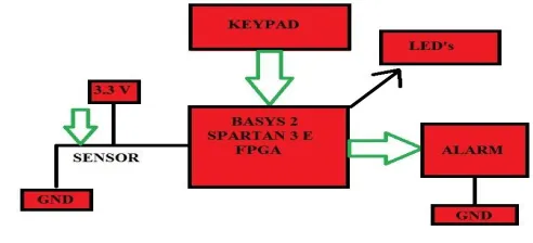
[image:2.612.149.395.572.684.2]The essential components that are used for the alarm system are Keypad for the entering the code, Sensors for sensing the code that is entered, Basys 2-Spartan 3E FPGA board, the Buzzer used as alarm.
Keypad here acts as input for the system from where the code is feed. The pushbuttons present on the basys 2 board is used as the keypad. The input is here is sensed by sensor in case the door or the window is open. The data from the sensor is send to FPGA in form of 1/0. If the sensor is open then 1 as the data is send to FPGA or-else sensor will be grounded. So 0 will be sent to FPGA. Here the alarm shown in the fig1 acts as the output. The Buzzer is installed in the Alarm and it will be activated in case the sensor is open and it sends the data ‘1’ in the FPGA. The system will have two states. First is the ‘Armed’ state and second is ‘Disarmed ‘state. The LED’s shown in the figure will indicate system is in Armed or Disarmed state.
The code entered through pushbutton will turn-on the LED, if code is wrong the alarm (Buzzer) will continue to ring. As the system is the 4-code system, the Led will glow sequentially as the code is entered.
III. DESIGN OF THE CODE-CHECKER
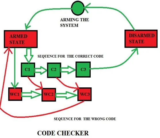
[image:3.612.144.422.250.490.2]The code checker is the pivotal part of the design for alarm system. Its function is to ensure that correct code is entered by the user. If the code-checker is not present in the system then it leads to malfunction. The code-checker has several states that is shown in the figure below.
Figure 2: Design for the Alarm System
The figure shows two states in the code checker that are the ‘Armed State and the ‘Disarmed State’. A user can shift the system from Armed to Disarmed State by entering correct sequence of code. The sequence for correct code is shown in the fig 2. The user enters code in sequence as C1, followed by C2 and C3, and the last code which disarms the system and it goes to Disarmed State. The cycle from Disarmed State can be armed as shown as “Arming the system” by entering two codes. Here if the first or the second code entered is wrong then system remains in Disarmed State. While if the system is working in the Armed State and if wrong codes are entered as shown in fig 2 (as WC1-WC2-WC3) it remains in Armed state and sensor senses the wrong codes and activates the alarm. (Sequence for the Wrong code is shown).
If the first code or second code is entered as correct codes and the other remaining codes are entered are wrong the pattern would follow the previous sequence i.e. Sequence for the Wrong code.
IV. FINITE STATE MACHINE TEMPLATE
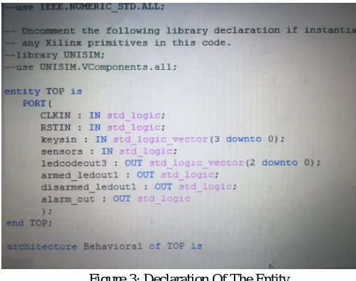
The family for FPGA used here is Spartan 3E and device is XC3S100E with package CP132. Here the VHDL module is used and different signals are used here. The system is made synchronous by addition of the clock (‘CLKIN’) signal in process. The reset (‘RSTIN’) signal is also given to reset the system to its initial parameters. The keys (pushbuttons) are represented in the entity as the “KEYSIN: STD_logic_vector (3 downto 0)” this represents the vector form for 4 keys.
Figure 3: Declaration Of The Entity
The output as declared in the entity as shown in the figure 3 are explained further. The ledcodeout3 is representation for the leds, it will glow if correct code is entered. They are represented in the vector form, as there are 3 leds. armed_ledout1 and disarmed_ledout1 are declared in the entity to represent ‘Armed State and the ‘Disarmed State’ respectively as explained in the design for the code checker. The alarm_out is shown which is used when “Arming the system”.
There are two choices for the selection of Finite state machine. “Mealy vs. Moore Styles” These are two well-known implementation styles for state-machines. The main difference between Mealy and Moore styles is the Mealy state-machine determines the output values based on both the current state as well as the inputs to the state-machine where Moore determines its outputs solely on the state. In general, Moore type of state-machines implement best in FPGAs and Mealy method for CPLDs (Complex programmable logic devices).
[image:4.612.125.484.489.672.2]Apart from it, in the design an addition Digital Clock Manager (DCM) is also added. It can be used as phase shift or as multiplication and division of the frequency and can increase or decrease the time duration. An Ip-core in ISE project navigator is selected for the purpose of addition of DCM to the design. In the design the input frequency for the external clock signal given is 50 MHz and the DCM converts this to 100 MHz by the Clk*2 multiplier which is further feed as the internal clock to the system. The figure shows the DCM where CLKIN is feed as 50 MHz and in the output CLK2X is selected which multiplies the frequency by 2. So the CLK2X signal acts as the input for the entire system, as the clock signal with frequency of 100 MHz.
.
Figure 4: Digital Clock Manager
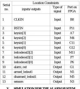
A. Addition of location constrains
1:
Serial no.
Location Constraints
inputs/ outputs Type of signal
Port on FPGA
1 CLKIN Input B8
2 RSTIN Input P11
3 keysin[3] Input A7
4 keysin[2] Input M4
5 keysin[1] Input C11
6 keysin[0] Input G12
7 ledcodeout3[2] Input M11
8 ledcodeout3[1] Input P7
9 ledcodeout3[0] Input P6
10 alarm_out Output G1
11 armed_ledout1 Output N5
12 disarmed_ledout1 Output M5
13 sensors Output N3
V. SIMULATION FOR THE ALARM SYSTEM
The simulation for the entire system is done, where system is is assumed to be unit under test (UUT). A test bench is created for this purpose. The UUT is instantiated as a module in the test bench.
The ISIM simulator is used for the alarm system simulation.
For the ISIM simulation the Netlist is converted to Simulation model. The steps for simulation includes the Behavioral/VHDL simulation for describing hardware. Post synthesis simulation is 2nd step for the process. Further post translate simulation and Post map simulation is carried. And the last step is Post (PAR) place and route simulation.
[image:5.612.178.435.87.373.2]The results for the simulation are shown below. For the codes that are entered in a pattern of 4-digit code as “0000, 0100, 1000, 1000, 0001”.
Figure 5: Simulation of Alarm System
[image:5.612.120.491.483.680.2]VI. CONCLUSION
This VLSI system is further modified for the many applications. It can be used in office for automatic door close system. The system can be used for automatic switching of street lights according to availability of daylight. It can also be used in automatic door lock system in houses, cars and offices after fixed time slot or fix duration. It can be used in remote interface which give a more reliable program. It is also use in industry in many applications. By adding video camera (for cost effective purpose), this system can be used as low cost home security system for apartments. We can provide 6V, 4 or 5 Ah battery back up to our system so that in case of power failure our project works properly The Alarm system implemented here on FPGA has many advantages in terms of inputs and outputs, power consumption, less wiring is used, comparatively a low cost system. The system is designed and implemented using VHDL language, which is the basic part of system. The location constraints are added to ease the process and system can be easily adjusted on FPGA.
A path toward ensuring the security of the tools and the resulting product is necessary to provide accountability throughout the development process.
REFERENCES
[1] Timothy Sherwood, Ryan Kastner, Timothy Levin, “Managing Security in FPGA Based Embedded Systems “
[2] Raqibull Hasan, Mohammad Monirujjaman Khan, “Microcontroller Based Home Security System with GSM Technology” [3] Madhuri R Mukkawar, S.D sawant “Home Automation through FPGA Controller”
[4] El-Medany, W.M. and El-Sabry, M.R. “GSM-Based Remote Sensing and Control System using FPGA”. Proceedings of International Conference on Computer and Communication Engineering Kuala Lumpur, 13-15 May 2008, 1093-1097.
[5] Van Der Werff, M., Gui, X. and Xu, W.L “A Mobile-Based Home Automation System” Proceedings of the 2nd International Conference on Mobile Technology, Applications and Systems. Guangzhou, 15-17 November 2005, 1-5.