Technology (IJRASET)
Design of Multiple Input DC-DC Converters
Manish Sharma1, Upendra Tomar2
Department of Electrical Engineering, Vikrant Institute of Technology& Mgmt, Gwalior Abstract- A new two-input DC-DC converter suitable to draw power from two different dc sources feeding a common dc-bus is
presented in this paper. This is a two-switch converter belongs to fifth-order family and performs bucking operation for one dc source while it allows both bucking as well as boosting feature with the second source. The salient feature of the proposed converter is that both the sources either individually or simultaneously supply power to the downstream load at reduced ripple current. This feature is particularly attractive for photovoltaic power processing applications. A digital voltage-mode controller is designed for downstream dc-bus regulation while the current controller regulates the power from the weak input power source. A 24 V, 100 Watt converter performance is analyzed and compared with the simulation observations.
I. INTRODUCTION
Reliability,accuracy and better load regulation are main issues of modern power supply .Demand of Switch-mode power converter is increasing day by day in various application such as hybrid vehicles and telecom power supply. .In order to utilize maximum energy from more than one energy source ,such as fuel cell.,battery,solar array and wind energy various multi input converter has been proposed in the recent year. Depending upon the applications one could select a feasible topology by considering many feature like reliability, cost and flexibility. Multi input converter has advantage of higher system efficiency high power density, light weight and small size.
A DC-to-DC converter is an electronic circuit or electromechanical device which converts a source of direct current (DC) from one voltage level to another. It is a type of electric power converter. Power levels range from very low (small batteries) to very high (high-voltage power transmission). DC -DC converter is one of the most important and widely used devices of modern power applications. Power electronics field in the last decade has been the development of switching-mode converters with higher power density and low electromagnetic interference. Light weight, small size and high power density are also some of the key design parameters. Several different types of switch-mode dc-dc converters belongs to buck, boost and buck-boost topologies, have been developed and reported in the literature to meet variety of applications . Major concern in the recent dc distribution systems, such as in automotive and telecom power supply systems, is to meet the increased power demand and reducing the load on the primary energy source, i.e. built-in battery. This is possible by adding additional power sources in parallel to the existing battery source. The additional power sources can be: (i) renewable energy sources such as photovoltaic (PV) or wind, (ii) fuel cell storage power The objective of this paper is to generate a two input topology by using pulsating source cell derived from six non isolated converter such as buck, boost buck-boost ,Cuk , SEPIC and Zeta. The single-ended primary-inductor converter (SEPIC) is a type of DC/DC converter allowing the electrical potential (voltage) at its output to be greater than, less than, or equal to that at its input. The output of the SEPIC is controlled by the duty cycle of the control transistor. A SEPIC is essentially a boost converter followed by a buck-boost converter, therefore it is similar to a traditional buck-boost converter, but has advantages of having non-inverted output (the output has the same voltage polarity as the input), using a series capacitor to couple energy from the input to the output (and thus can respond more gracefully to a short-circuit output), and being capable of true shutdown: when the switch is turned off, its output drops to 0 V . SEPICs are useful in applications in which a battery voltage can be above and below that of the regulator's intended output. For example, a single lithium ion battery typically discharges from 4.2 volts to 3 volts; if other components require 3.3 volts, then the SEPIC would be effective.
Technology (IJRASET)
power supply systems, is to meet the increased power demand and reducing the load on the primary energy source, i.e. built-in battery. This is possible by adding additional power sources in parallel to the existing battery source. The additional power sources can be: (i) renewable energy sources such as photovoltaic (PV) or wind, (ii) fuel cell storage power. Power sources supplementing other resources are normally categorized as hybrid power source and the corresponding scheme is called hybrid distributed generation systems. DC to DC converters are used in portable electronic devices such as cellular phones and laptop computers, which are supplied with power from batteries primarily. DC-to-DC techniques that use transformers or inductors work at much higher frequencies, requiring only much smaller, lighter, and cheaper wound components. Consequently these techniques are used even where a mains transformer could be used; for example, for domestic electronic appliances it is preferable to rectify mains voltage to DC, use switch-mode techniques to convert it to high-frequency AC at the desired voltage, then, usually, rectify to DC. The entire complex circuit is cheaper and more efficient than a simple mains transformer circuit of the same output.
Integration of renewable energy sources to form a distributed generation system is a viable option for the hybrid vehicles, automotive industries and even in remote stand-alone power supply system. In order to efficiently and economically utilize renewable energy resources it is necessary to tap the energy as and when it is available and then store for subsequent utilization. Nowadays, electric double layer capacitors are coming up in the energy storage systems in addition to the conventional battery systems. However, in all these cases the power conversion efficiency and it’s control is major challenge for the power supply designer. The efficiency improvement with higher power density, from the steady-state point of view, of the distributed energy generation is one of the considerations for the designer. The other constraint while designing such system is to evolve simple and reliable power control strategy.
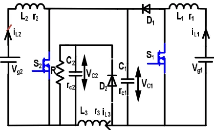
[image:3.612.203.422.405.538.2]To address some of the above issues, multi-input converters, with different topology combinations, are evolving. Although several power conversion topology configurations can easily be developed, but an integrated converter with bucking, buck-boost feature is desired in most of these schemes. To this affect, there is not enough literature covering the development of converter and control schemes for such applications. Furthermore, literature covering design aspects of digital controllers for such kinds of converters is also limited. In order to bridge this gap, a new two-input dc-dc converter is proposed in this paper and then digital controllers have been designed to ensure dc-bus voltage regulation together with power distribution control of the input dc power sources.
Fig. 1. DC-DC CONVERTER CIRCUIT DIAGRAM
Several compensator design approaches have been reported in the literature for Op-Amp or IC based analogue controllers. However, in the case of digital controller design, two main approaches are widely used, that is: (i) digital redesign method (DRM), (ii) direct digital design method (DDDM). In the first case, the compensator is designed in the conventional way by using s-domain transfer functions together with linear system theory and the resulting compensator is transformed into the digital domain using appropriate z-transformations. On the other hand, in DDDM, the compensator design is carried out in the z-domain itself and hence there is no need for s -to- z-domain transformation. In view of these features here DDDM is used for the robust digital controller design.
II. MODELINGOFTWO-INPUTDC-DCCONVERTER
Technology (IJRASET)
of operation.Depending upon the magnitude of duty ratios ,three different scheme are possible. Scheme 1:d1>d2 Scheme 2: d1<d2 and Scheme 3: d1=d2. In first scheme (d1>d2) The circuit is going to operate under four different modes in one switching cycle .In this paper scheme 2(d1<d2) is considered in which circuit exhibits three mode operation in one switching cycle In the power conversion process it performs boosting operation for one dc source, buck-boost conversion for the second source. It has the following salient features (a) both the dc sources are supplying continuous currents and hence their ripple current is low, (b) lesser filtering requirement on the input side, (c) automatic load transfer on to the first dc source if the second dc source capacity, weak source with limited power supplying capacity, is less than the load demand, and (d) simple control strategy, with or without overlap of duty ratio signals, as there are only two switching devices need to be controlled.
For scheme 2 (d2>.d1) converter exhibits three mode of operation in a switching cycle .(a) mode-1:S1,S2 both are ON and diode D1,d2 are OFF.(b) 2:S2,D1 are ON and S1,D2 are OFF.(c)3:S1,S2 both are OFF and D1,D2 both are ON.During mode-1 inductor Lmode-1 and L2 are linealy charging by there respective sourse voltages Vgmode-1 and Vg2 and capacitor Cmode-1 charges inductor L3,capacitor C2 discharges through load.In mode-2 inductor L2 charges linearly and inductor L1 discharges through capacitor C1 and energy stored in inductor L1 will transferred to buffer capacitor C1 .In mode-3 energy stored in capacitor C1 and second energy source (Vg2) will transfer power to the load simultaneously.
So dynamics of the system can be described by the set of state space equation in each mode is given by The circuit can operate either in continuous or discontinuous inductor current mode. But, the proposed converter is mainly for higher load power requirement, where one dc source unable to meet the complete load demands and hence the inductor currents are almost all the times are continuous. In view of this the converter is analyzed here for continuous current mode of operation. Here the circuit operation also depends on the type of controlling signal used for switching devices S1 and S2, and the two switching devices, (S1 and S2), can be synchronized either with trailing-edge or leading edge operation. Each of these schemes has their own advantages and limitations and detailed discussion on the suitability and application requirements will be discussed in the final paper. Furthermore,
depending on the load demand and available power with each dc source three different cases will arise, which are: (i)
d
1
d
2,
(ii)1 2
,
d
d
(iii)d
1
d
2.
In the first two cases the circuit undergoes three different structural changes, while in the last case only twodifferent operating modes in one switching cycle. In this paper the
d
1
d
2case is analyzed for the trailing-edge synchronizedswitching signals. Applying volt-sec balance to inductors gives the voltage conversion ratio of this converter as
1 1 2 2
1
2.
o
V
V d
V d
d
From this equation it is clear that the load voltage is controlled by the both the switch duty ratiosignals and also depends on both input dc sources. The analysis of the remaining two different cases is quite similar to one
presented in this paper. For
d
1
d
2case the switching sequence in one switching cycle is: (i) mode-1: S1 and S2 both ON, (ii)mode-2: S1-ON and S2-OFF, (iii) mode-3: Diode- ON. In each mode of operation the power stage dynamics can easily be described by a set of state equations given by:
u
B
x
A
x
K
Kk k
y
C x
F u
(1)where
1 2 3 1 2 ,T
L L L c c
x i i i v v
1 2 ,T
g g
u V V
and k=1,2,3 for mode-1, mode-2 and 3, respectively.
The above equation describes the small-signal dynamics of the proposed converter, with the converter state variables depending on the two control variables, d1 and d2. In order to design suitable control strategies based on d1 and d2, it is essential to know the degree of interaction between the control loops. Details of control loop interactions using relative gain array theory and loop design aspects will be discussed in the final paper.
III. DIGITALCONTROLLERDESIGN
Technology (IJRASET)
The control schemes can be interchangeable from one to other depending on the source power supply capacity. However, use of current-control loop for heavier source limits the load supplying capacity and hence it is not recommended. In view of this difficulty it is always recommended to use current-control loop for the weaker source and connected to the circuit portion that gives buck-boost feature. DC-bus voltage regulation loop should be closed together with the heavier source. Detailed mathematical treatment will be presented in the final paper to support above discussion. For decoupled digital controllers design two different loopgains have been defined here, one for current-control loop while the second one for the dc-bus voltage regulation loop. In any case the digital compensator is designed using sisotool of the MATLAB in the frequency domain. Pole-zero placement technique is used and then final design is arrived. Fine tuning of the compensator is performed to ensure relative stability margins, i.e. gain margin> 6 dB, 350<phase margin<750 and reasonable crossover frequency, which normally depends on the order of the converter under consideration.
0.0506(
0.97)
( )
(
1)
ciz
G
z
z
(2)13.502(
0.8384)(
0.8326)
( )
(
1)(
0.272)
cvz
z
G
z
z
z
(3)IV. SIMULATIONSTUDIESANDEXPERIMENTALRESULTS
To extract the salient features of the proposed converter and to verify the load distribution together with dc-bus regulation capability a 24 V, 96 Watt two-inputdc-dc converter system was considered in this studies and its parameters are listed in Table I. PSIM is used for simulation purpose. In these studies DC source-1 considered as heavier source having sufficient power supplying capacity, more than load demand, while DC source-2 considered as weaker source with its power supplying capacity less than the load demand.
For a load demand 96 W, the load distribution pattern on the two input dc sources is shown in Fig. 5. In this simulation it has been kept current limit of 2 A on the dc source-2 and its maximum power delivering capacity is 24 W. In the load demand of 96 W dc-source-1 supplies 72 W, while source-2 supplies 24 W. When the dc source-2 supplying its full rated power then any additional load coming on to the converter is going reflect on dc source-1. To illustrate this feature the load resistance is changed from 6 to 4 Ω and
the corresponding results are shown in Fig. 6. It is clear from the simulation results that load voltage is almost constant and the additional load demand is transferred on the dc source-1.
0 10 20 30 40 50 60 V0 0 1 2 3 4 I(R)
0 0.005 0.01 0.015 0.02 0.025 0.03
Ti me (s) 35 36 37 38 39 40 Vg2
Technology (IJRASET)
V. CONCLUSION
A new two-input DC-DC converter suitable for drawing power from two different dc sources and feeding to common dc bus was proposed in this paper. Modes of operations have been analyzed and then decoupled control-loops were designed to distribute the load demand on both the input sources. Voltage-mode control strategy was used to ensure dc bus voltage regulation, while current-control loop was implemented to restrict the load division on the second source. Simulation and experimental results were in agreement with the theoretical predictions. Detailed comparison of simulation and experimental results for different conditions will be given in the final paper.
REFERENCES
[1] Hirofumi Matsuo, Wenzhong Lin, Fujio Kurokawa, Tetsuro Shigemizu, Nobuya Watanabe, “Characteristics of the Multiple-Input DC–DC Converter,” IEEE Trans. on Ind. Electron, vol. 51, no. 3, pp.625-631, Jun. 2004.
[2] Jian Liu, Zhiming Chen, Zhong Du, “A new design of power supplies for pocket computer system”, IEEE Trans. on Ind. Electronics, 1998, Vol. 45(2), pp. 228-234.
[3] K. P. Yalamanchili, M. Ferdowsi, Keith Corzine, “New Double input dc-dc converters for automotive applications", IEEE Applied Power Electronics Conference (APEC), 2006, CD-ROM proceddings.
[4] R. D. Middlebrook, Cuk. S, “A general unified approach to modelling switching converter power stage”, IEEE Power electronics specialists conference, 1976, pp. 13-34.
[5] D. Maksimovic and R. Zane, “Small-Signal Discrete Time Modeling of Digitally Controlled PWM Converters”, IEEE Trans. on Power Electronics, vol. 22, no. 6, pp. 2552-2556, Jun. 2007.
[6] Krishna Mohan. B, “Robust Digital Voltage Mode Controller for Fifth-Order Boost Converter,” IEEE Trans. Industrial Electron., vol. 58, no. 1, pp. 263-277, Jan.2010.
[7] M. Veerachary, “Two-loop controlled buck-SEPIC converter for input source power management,” IEEE Trans. On Industrial Electronics, Vol. 59(11), pp. 4075-4087, 2012.