Implementation of an Efficient Multiplier Architecture
over a Conventional Methods using Ancient Indian Vedic
Sutra
Bhushan M. Shelke
LecturerNUVA C.E.T.,R.T.M.N.U. Nagpur,Maharashtra (INDIA)
Shubhangi A. Wakode
LecturerNUVA C.E.T.,R.T.M.N.U. Nagpur,Maharashtra (INDIA)
ABSTRACT
Fast multiplication is very important in processing of digital signals like DSP for convolution, Fourier Transform, etc. Many conventional methods are used for designing a multiplier for processing a digital signal. In this paper, A fast method for multiplication based on Ancient Indian Vedic mathematics is proposed. The whole of Vedic mathematics is based on 16 sutras (formulae). Among the various methods of multiplication in Vedicmathematics, Urdhava Tiryakbhyam (Vertically and Crosswise) is discussed in detail. This is the general multiplication formula applicable to all cases of multiplication. For implimentation of a efficient Architecture simple Boolean logic is combined with Vedic formulas, which reduces the partial products and sums generated in one step.The coding is done in VHDL and synthesis is done using Xilinx ISE 9.1i simulator. Results are compaired with several conventional techniques.
Keywords
Vedic mathematics, Sutra,Urdhava Tiryakbhyam, VHDL.
1.
INTRODUCTION
The Vedic Mathematics approach is totally different and considered very close to the way a human mind works. In this work, try to present multiplication operations and the implementation of these using both conventional, as well as Vedic mathematical methods in VHDL (VHSIC Hardware Description Language). Vedic mathematics is the name given to the ancient system of mathematics, a unique technique of calculations based on simple rules and principles with which any mathematical problem can be solved like arithmetic, algebra, geometry or trigonometry. Vedic Mathematics (1965), which is considered the starting point for all work on Vedic mathematics. It was rediscovered from the ancient Indian scriptures between 1911 and 1918 by Sri Bharati Krishna Tirthaji (1884-1960), a scholar of Sanskrit, mathematics, history and philosophy [1]. Conventional mathematics is an integral part of engineering education since most engineering system designs are based on various mathematical approaches. The need for faster processing speed is continuously driving major improvements in processor technologies, as well as the search for new algorithms. A multiplier is one of the key hardware blocks in most digital signal processing systems [2]. Performing athematical calculations especially multiplication, a computer spends a considerable amount of its processing time, an improvement in the speed of a math coprocessor for performing multiplication will increase the overall speed of the computer. The multiplier is a fairly large block of a
computing system. The amount of circuitry involved is directly proportional to the square of its resolution i.e. A
multiplier of size ‘N’ bits has ‘N^2’ gates. Apply Vedic Sutras to binary multipliers using carry adders.
In particular, develop an efficient binary multiplier architecture that performs partial product generations and additions. Here, the computation time involved is less. The combinational delay and the device utilizations obtained after synthesis is compared. The proposed Vedic multiplier based Circuit seems to have better performance in terms of speed.
1.1 Urdhava Ti ryakbhy am
S u t r a [image:1.595.322.533.440.568.2]The meaning of this sutra is “Vertically and crosswise” and it is applicable to all the multiplication operations. Figure 1 represents the general multiplication procedure of the 4×4 decimal digit multiplication. Let us consider the multiplication of two decimal numbers (1234 × 8765).
Figure 1 : Multiplication implementation using Urdhva Tiryakbhyam Sutra [3].
get 7 as the sum and set it down as the middle part of the answer. Then 2 and 3 is multiplied vertically, get 6 as their product and put it down as the last the left hand most part of the answer.
Figure 2 : Multiplication of 21 X 32 using Urdhva Tiryakbhyam Sutra.
1.1.1 Mathematical representation of Urdhava
Ti ryakbhyam sut ra
Assume that X and Y are two numbers, to be multiplied. Mathematically X and Y can be represented as:
,
Assume that, their product is equal to Z. Then Z can be represented as:
Where (Ai , Bj € (0,1,2,...,9) and ‘N’ may ne any number [4]. From the above expression, it can observed that each digit is multiplied consecutively and shifted towards the proper positions for partial product generation. Finally the partial products are added with the previous carry to produce the final results.
1.1.2 Bi nary real i zat i o n of Urdhav a
Ti ryakbhyam sut ra
Cosider a 8X8 bit binary number as A and B. So, bit multiplication will be as follows.
A = A7A6A5A4A3A2A1A0
B = B7B6B5B4B3B2B1B0
Make the partition into equal part of A and B.
AH = A7A6A5A4,
AL = A3A2A1A0.
BH = B7B6B5B4,
BL = B3B2B1B0.
Finally, according to Urdhava Tiryakbhyam Sutra,
A×B=AL×BL+AH×BL+AL×BH+AH×BH
The final equition shows the result multiplication using Vedic Sutra.
2.
DESIGN & IMPLEMENTATION
The Vedic multiplier is implemented using VHDL and also other multipliers like booth multiplier and shift-add multiplier are also implemented. VHDL code is completely synthesizable. The synthesis is done using Xilinx Synthesis
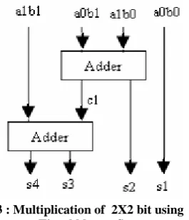
Tool (XST) available with Xilinx ISE 9.1i. The design starts first with Multiplier design, that is 2X2 bit multiplier as shown in figure 3. Here, “Urdhva Tiryakbhyam Sutra” Algorithm for multiplication has been effectively used to develop digital multiplier architecture. This algorithm is quite different from the traditional method of multiplication, which is to add and shift the partial products.
Figure 3 : Multiplication of 2X2 bit using Urdhva Tiryakbhyam Sutra.
For Multiplier, first the basic blocks, that are the 2x2 bit multipliers have been made and then, using these blocks, 4x4 block has been made by adding the partial products using adder circuits and then using this 4x4 block the 8x8 bit multipler block is implemented. The figure 4 shows implementation of 8X8 bit multiplier using Urdhava Tiryakbhyam sutra. The 8 bit input A and B are given to the 4X4 vedic multiplier block which generate the output to be manipulate into adder circuit to obtained the output given as,
[image:2.595.362.495.154.309.2]X×Y = ( Z1 5- Z8) & ( Z7- Z4) & ( Z3- Z0)
Figure 4 : Hardware realization of 8x8 bit multiplication using Urdhava Tiryakbhyam Sutra.
The architecture of 16X16 Vedic multiplier using Urdhva Tiryagbhyam Sutra is shown in Figure 5. The 16X16 Vedic multiplier architecture is implemented using four 8x8 Vedic multiplier modules and two16 bit binary adder stages. The resultant output is given as,
[image:2.595.322.537.446.596.2]Figure 5 : H a r d w a r e r e a l i z a t i o n o f 1 6 x 1 6 b i t m u l t i p l i c a t i o n u s i n g U r d h a v a T i r y a k b h y a m
S u t r a .
Finally, 32X32 bit Vedic Multiplier as shown in figure 6 has been made using the four 16X16 bit Vedic multiplier modules and two 32 bit binary adder stages. The resultant output is given as,
[image:3.595.58.271.341.483.2]X×Y = ( Z6 3- Z3 2) & ( Z3 1- Z1 6) & ( Z1 5- Z0)
Figure 6 : H a r d w a r e r e a l i z a t i o n o f 3 2 x 3 2 b i t m u l t i p l i c a t i o n u s i n g U r d h a v a T i r y a k b h y a m
S u t r a .
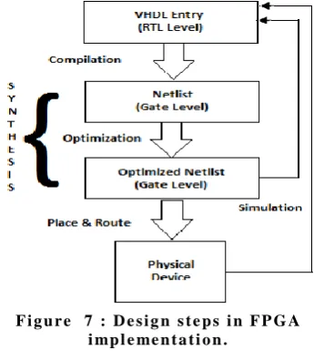
2.1 Design steps in FPGA implementation
FPGA (Field Programable Gate Array) device is used for implementation of Vedic Multiplier designed using HDL (Hardware Description Language), here it is VHDL. As shown in figure 7, there are four basic building blocks in FPGA implementation.
1. The design starts with VHDL Entry level refers to RTL level.
2. The design compilation producess Netlist upto the Gate level.
3. Optimization process designed the optimized view of optimized Gate structure.
4. This stage helps to prove the manifests of the design structure by simulation process.
5. The combination of step (2) and (3) equally called as Synthesis Process.
6.Final stage is the implementation on physical device with the help of Place and Route process.
7. As the FPGA device is reconfigurable, the entire procedure can be done several times.
F i g u r e 7 : D e s i g n s t e p s i n F P G A i mp l e me n t a t i o n .
3.
RESULTS AND DISCUSSION
In this work the algorithms are implemented in VHDL and logic simulations are done using Xilinx project navigator vession 9.1i. The Xilinx families are used for simulation are as given below,
Xilinx : Spartan3 3s50pq208-5.
Xilinx : Vertex2P 2vp2fg256-7.
T a b l e 1 : V e d i c mu l t i p l i e r u s i n g U r d h a v a T i r y a k b h y a m S u t r a – C o m b i n a t i o n a l D e l a y i n
V a r i o u s D e v i c e s ( n s ) .
D e v i c e 8 X 8 1 6 X 1 6 3 2 X 3 2
S p a r t a n 3
s 5 0 p q 2 0 8 - 5 . 2 3 . 4 2 2 4 3 . 3 9 8 7 9 . 8 4 8
V e r t e x 2 P
[image:3.595.341.514.346.544.2]T a b l e 2 : S h i f t - A d d mu l t i p l i e r - C o mb i n a t i o n a l D e l a y i n V a r i o u s D e v i c e s ( n s ) .
D e v i c e 8 X 8 1 6 X1 6 3 2 X3 2
S p a r t a n 3
3 s 5 0 p q 2 0 8 - 5 . 2 7 . 1 3 3 5 0 . 9 6 8 9 6 . 3 5 2
V e r t e x 2 P
2 v p 2 f g 2 5 6 - 7 . 1 4 . 8 7 5 2 7 . 2 4 0 5 1 . 1 8 2
T a b l e 3 : B o o t h mu l t i p l i e r - C o mb i n a t i o n a l D e l a y i n V a r i o u s D e v i c e s ( n s ) .
D e v i c e 8 X 8 1 6 X1 6 3 2 X 3 2
S p a r t a n 3
3 s 5 0 p q 2 0 8 - 5 . 2 5 . 7 5 6 5 9 . 2 3 8 1 1 7 . 8 4 3
V e r t e x 2 P
2 v p 2 f g 2 5 6 - 7 . 1 5 . 8 1 5 3 6 . 0 7 1 6 3 . 7 4 1
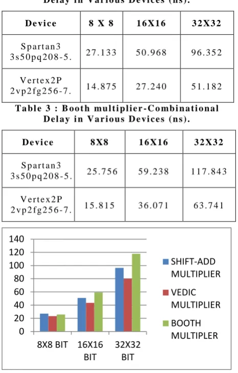
F i g u r e 8 : G r a f i c a l r e p r e s e n t a t i o n o f c o mb i n a t i o n a l d e l a y ( n s ) f o r X i l i n x S p a r t a n 3
( 3 s 5 0 p q 2 0 8 - 5 ) f a mi l y f r o m T a b l e 1 , 2 , 3 .
From figure 8, it is seen that the vedic multiplier requires less time than conventional multipliers. The efficiency of Vedic Multiplier for each method is obtained, as shown in table 4.
T a b l e 4 : E f f i c i e n c y o f V e d i c mu l t i p l i e r o v e r a c o n v e n t i o n a l me t h o d f o r X i l i n x S p a r t a n 3
( 3 s 5 0 p q 2 0 8 - 5 ) f a mi l y f r o m t a b l e 1 , 2 , 3 .
T e c h n i q u e 8 X8 1 6 X1 6 3 2 X 3 2
S h i f t a d d
M e t h o d 1 3 . 6 7 % 1 4 . 8 5 % 1 7 . 1 2 %
B o o t h
M e t h o d 1 2 . 8 5 % 1 4 . 7 1 % 1 7 . 0 7 %
F i g u r e 9 : G r a f i c a l r e p r e s e n t a t i o n o f c o mb i n a t i o n a l d e l a y ( n s ) f o r X i l i n x V e r t e x 2 P
( 2 v p 2 f g 2 5 6 - 7 ) f a mi l y f r o m T a b l e 1 , 2 , 3 .
Simillarly, Figure 9 shows the efficient result of Vedic Multiplier for a Combinational delay over a conventional methods and it is numericaly shown in table 5.
T a b l e 5 : E f f i c i e n c y o f V e d i c mu l t i p l i e r o v e r a c o n v e n t i o n a l me t h o d s f o r X i l i n x V e r t e x 2 P
( 2 v p 2 f g 2 5 6 - 7 ) f a mi l y f r o m t a b l e 1 , 2 , 3 .
T e c h n i q u e 8 X 8 1 6 X 1 6 3 2 X 3 2
S h i f t a d d
M e t h o d 0 9 . 0 6 % 2 6 . 7 3 % 3 2 . 2 4 %
B o o t h
M e t h o d 1 8 . 0 3 % 3 5 . 5 7 % 3 6 . 4 1 %
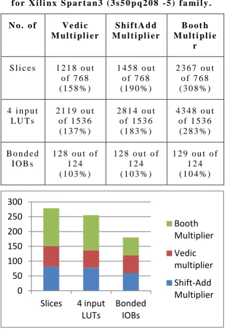
From table 4 and 5, it is seen that as increase in the number of input bits, the performance of the Vedic Multiplier is gradualy increases. As shown in table 4 and 5, the Shift-Add multiplier is more efficient than Booth multiplier in time utilization. This is also observed that the utilization of space is effectively efficient in Vedic Multiplier over a Conventional Multipliers. Validation of space efficiency is proven by Xilinx simulator. The obtained results are shown in table 6,7,8 for Xilinx Spartan3 (3s50pq208-5) family.
T a b l e 6 : D e v i c e U t i l i z a t i o n S u m m a r y o f 8 X 8 b i t V e d i c a n d C o n v e n t i o n a l M u l t i p l i e r f o r
X i l i n x S p a r t a n 3 ( 3 s 5 0 p q 2 0 8 - 5 ) f a mi l y .
N o . o f V e d i c M u l t i p l i e r
S h i f t A d d M u l t i p l i e r
B o o t h M u l t i p l i e
r [ 5 ]
S l i c e s 6 6 o u t o f 7 6 8 ( 8 % )
6 8 o u t o f 7 6 8 ( 8 % )
9 6 o u t o f 7 6 8 ( 1 2 % )
4 i n p u t L U T s
1 1 4 o u t o f 1 5 3 6 ( 7 % )
1 1 9 o u t o f 1 5 3 6 ( 7 % )
1 7 8 o u t o f 1 5 3 6 ( 1 2 % )
B o n d e d I O B s
3 2 o u t o f 1 2 4 ( 2 5 % )
3 2 o u t o f 1 2 4 ( 2 5 % )
3 2 o u t o f 1 2 4 ( 2 5 % )
0 20 40 60 80 100 120 140
8X8 BIT 16X16 BIT
32X32 BIT
SHIFT-ADD MULTIPLIER
VEDIC MULTIPLIER
BOOTH MULTIPLER
0 10 20 30 40 50 60 70
8X8 BIT 16X16 BIT
32X32 BIT
SHIFT-ADD MULTIPLIER
VEDIC MULTIPLIER
[image:4.595.315.545.72.231.2] [image:4.595.52.285.88.453.2] [image:4.595.315.544.330.425.2]T a b l e 7 : D e v i c e U t i l i z a t i o n S u m m a r y o f 1 6 X 1 6 b i t V e d i c a n d C o n v e n t i o n a l M u l t i p l i e r
f o r X i l i n x S p a r t a n 3 ( 3 s 5 0 p q 2 0 8 - 5 ) f a mi l y .
N o . o f V e d i c M u l t i p l i e r
S h i f t A d d M u l t i p l i e
r
B o o t h M u l t i p l i e
r [ 5 ]
S l i c e s 3 1 0 o u t o f 7 6 8 ( 4 0 % )
3 6 7 o u t o f 7 6 8 ( 4 7 % )
4 9 9 o u t o f 7 6 8 ( 6 5 % )
4 i n p u t L U T s
5 4 1 o u t o f 1 5 3 6 ( 3 5 % )
6 4 1 o u t o f 1 5 3 6 ( 4 2 % )
9 2 3 o u t o f 1 5 3 6 ( 6 0 %
)
B o n d e d I O B s
6 4 o u t o f 1 2 4 ( 5 1 % )
6 4 o u t o f 1 2 4 ( 5 1 % )
6 5 o u t o f 1 2 4 ( 5 2 % )
T a b l e 8 : D e v i c e U t i l i z a t i o n S u m m a r y o f 3 2 X 3 2 b i t V e d i c a n d C o n v e n t i o n a l M u l t i p l i e r
f o r X i l i n x S p a r t a n 3 ( 3 s 5 0 p q 2 0 8 - 5 ) f a mi l y .
N o . o f V e d i c M u l t i p l i e r
S h i f t A d d M u l t i p l i e r
B o o t h M u l t i p l i e
r
S l i c e s 1 2 1 8 o u t o f 7 6 8 ( 1 5 8 % )
1 4 5 8 o u t o f 7 6 8 ( 1 9 0 % )
2 3 6 7 o u t o f 7 6 8 ( 3 0 8 % )
4 i n p u t L U T s
2 1 1 9 o u t o f 1 5 3 6 ( 1 3 7 % )
2 8 1 4 o u t o f 1 5 3 6 ( 1 8 3 % )
4 3 4 8 o u t o f 1 5 3 6 ( 2 8 3 % )
B o n d e d I O B s
1 2 8 o u t o f 1 2 4 ( 1 0 3 % )
1 2 8 o u t o f 1 2 4 ( 1 0 3 % )
1 2 9 o u t o f 1 2 4 ( 1 0 4 % )
F i g u r e 1 0 : G r a f i c a l r e p r e s e n t a t i o n o f a v e r a g e d e v i c e u t i l i z a t i o n ( % ) f o r Xi l i n x S p a r t a n 3
( 3 s 5 0 p q 2 0 8 - 5 ) f a mi l y f r o m T a b l e 6 , 7 , 8 .
Similar results are obtained for the validation of space efficiency of Vedic Multiplier over a Shift-Add and Booth Multiplier by using Xilinx Vertex2P (2vp2fg256-7) family and it is shown in table 9,10,11.
T a b l e 9 : D e v i c e U t i l i z a t i o n S u m m a r y o f 8 X 8 b i t V e d i c a n d C o n v e n t i o n a l M u l t i p l i e r f o r
X i l i n x V e r t e x 2 P ( 2 v p 2 f g 2 5 6 - 7 ) f a mi l y .
N o . o f V e d i c M u l t i p l i e r
S h i f t A d d M u l t i p l i e r
B o o t h M u l t i p l i e
r
S l i c e s 7 6 o u t o f 1 4 0 8 ( 5 % )
8 1 o u t o f 1 4 0 8 ( 6 % )
1 1 7 o u t o f 1 4 0 8 ( 8 % )
4 i n p u t L U T s
1 3 3 o u t o f 2 8 1 6 ( 5 % )
1 7 3 o u t o f 2 8 1 6 ( 6 % )
1 9 8 o u t o f 2 8 1 6 ( 7 % )
B o n d e d I O B s
3 2 o u t o f 1 4 0 ( 2 2 % )
3 2 o u t o f 1 4 0 ( 2 5 % )
3 3 o u t o f 1 4 0 ( 2 3 % )
T a b l e 1 0 : D e v i c e U t i l i z a t i o n S u m m a r y o f 1 6 X1 6 b i t V e d i c a n d C o n v e n t i o n a l M u l t i p l i e r
f o r X i l i n x V e r t e x 2 P ( 2 v p 2 f g 2 5 6 - 7 ) f a mi l y .
N o . o f V e d i c M u l t i p l i e r
S h i f t A d d M u l t i p l i e r
B o o t h M u l t i p l i e
r
S l i c e s 3 1 0 o u t o f 1 4 0 8 ( 2 2 % )
3 8 5 o u t o f 1 4 0 8 ( 2 7 % )
4 1 7 o u t o f 1 4 0 8 ( 2 9 % )
4 i n p u t L U T s
5 4 1 o u t o f 2 8 1 6 ( 1 9 % )
5 9 5 o u t o f 2 8 1 6 ( 2 1 % )
6 3 9 o u t o f 2 8 1 6 ( 2 3 % )
B o n d e d I O B s
6 4 o u t o f 1 4 0 ( 4 5 % )
6 4 o u t o f 1 4 0 ( 4 5 % )
6 5 o u t o f 1 4 0 ( 4 6 % )
T a b l e 1 1 : D e v i c e U t i l i z a t i o n S u m m a r y o f 3 2 X3 2 b i t V e d i c a n d C o n v e n t i o n a l M u l t i p l i e r
f o r X i l i n x V e r t e x 2 P ( 2 v p 2 f g 2 5 6 - 7 ) f a mi l y .
N o . o f V e d i c M u l t i p l i e r
S h i f t A d d M u l t i p l i e r
B o o t h M u l t i p l i e
r
S l i c e s 1 2 1 8 o u t o f 1 4 0 8
( 8 6 % )
1 9 5 8 o u t o f 1 4 0 8
( 1 3 9 % )
2 3 6 7 o u t o f 1 4 0 8
( 1 6 8 % )
4 i n p u t L U T s
2 1 1 9 o u t o f 2 8 1 6
( 7 5 % )
3 3 1 4 o u t o f 2 8 1 6
( 1 1 8 % )
4 3 4 8 o u t o f 2 8 1 6
( 1 5 4 % )
B o n d e d I O B s
1 2 8 o u t o f 1 4 0 ( 9 1 % )
1 2 8 o u t o f 1 4 0 ( 9 1 % )
1 2 9 o u t o f 1 4 0 ( 9 2 % )
0 50 100 150 200 250 300
Slices 4 input
[image:5.595.315.543.83.696.2] [image:5.595.53.284.307.645.2]The grafical representation of average device utilization is shown in figure 11 for the simulation results shown in table 9,10,11.
F i g u r e 1 1 : G r a f i c a l r e p r e s e n t a t i o n o f a v e r a g e d e v i c e u t i l i z a t i o n ( % ) f o r Xi l i n x Ve r t e x 2 P
( 2 v p 2 f g 2 5 6 - 7 ) f a mi l y f r o m T a b l e 6 , 7 , 8 .
F i g u r e 1 2 : G r a f i c a l r e p r e s e n t a t i o n o f t o t a l me m o r y u s a g e ( M e g a b y t e ) f o r X i l i n x S p a r t a n 3
( 3 s 5 0 p q 2 0 8 - 5 ) f a mi l y .
F i g u r e 1 3 : G r a f i c a l r e p r e s e n t a t i o n o f t o t a l me m o r y u s a g e ( M e g a b y t e ) f o r X i l i n x V e r t e x 2 P
( 2 v p 2 f g 2 5 6 - 7 ) f a mi l y .
Figure 12 and 13 are based on the result obtained for the total memory usages by FPGA family used for synthesis using Xilinx Simulator.
The simulation results for a 8X8 bit,16X16 bit, 32X32 bit Vedic Multipliers using Vedic Sutra Urdhava Tiryakbhyam is shown in figure 14,15,16 respectively.
F i g u r e 1 4 : T h e r e s u l t s o f 8 X8 b i t mu l t i p l i c a t i o n b y V e d i c M u l t i p l i e r u s i n g U r d h a v a T i r y a k b h y a m S u t r a .
F i g u r e 1 5 : T h e r e s u l t s o f 1 6 X1 6 b i t mu l t i p l i c a t i o n b y V e d i c M u l t i p l i e r u s i n g U r d h a v a T i r y a k b h y a m S u t r a .
F i g u r e 1 6 : T h e r e s u l t s o f 3 2 X3 2 b i t mu l t i p l i c a t i o n b y V e d i c M u l t i p l i e r u s i n g U r d h a v a T i r y a k b h y a m S u t r a .
4.
CONCLUSIONS
The performance of the proposed multiplier using Vedic Sutra proved to be efficient in terms of speed, space and power. As the input bits increases, relatively the efficiency of the circuit is also increases. The main advantage is delay increases slowly as input bits increase. It is also demonstrated that this
design is quite efficient in terms of silicon area/speed. By using these ancient Indian Vedic mathematics techniques, the world can reach new heights of performance and excellence for the cutting edge technology devices.
0 50 100 150 200
Slices 4 input
LUTs
Bonded IOBs
Booth Multiplier
Vedic Multiplier
Shift-Add Multiplier
0 50 100 150 200 250 300 350
8X8 BIT 16X16 BIT
32X32 BIT
Shift-Add Multiplier
Vedic Multiplier
Booth Multiplier
0 100 200 300 400
8X8 BIT 16X16 BIT
32X32 BIT
Shift-Add Multiplier
Vedic Multiplier
[image:6.595.54.525.100.504.2] [image:6.595.315.546.104.247.2] [image:6.595.53.282.110.244.2]5.
REFERENCES
[1] Vedic mathematics or sixteen simple mathematical formulae from the Vedas by Jagadguru Swami Shri Bharati Krishna Tirthaji Maharaja, General Editor – Dr. V. S. Agrawal , First Edition : Varanasi ,1965.
[2] Kabiraj Sethi , Rutuparna Panda : “An Improved Squaring Circuit for Binary Numbers”, (IJACSA) International Journal of Advanced Computer Science and Applications, Vol. 3, No.2, 2012.
[3] G.Ganesh Kumar, V.Charishma : “Design of High Speed Vedic Multiplier using Vedic Mathematics Techniques”, International Journal of Scientific and Research
Publications, Volume 2, Issue 3, March 2012 ISSN 2250-3153.
[4] P. Saha, A. Banerjee, A. Dandapat, P. Bhattacharyya :” Vedic Mathematics Based 32-Bit Multiplier Design for High Speed Low Power Processors”, international journal on smart sensing and intelligent systems vol. 4,No. 2 june 2011.
![Figure 1 : Multiplication implementation using Urdhva Tiryakbhyam Sutra [3].](https://thumb-us.123doks.com/thumbv2/123dok_us/8068567.778785/1.595.322.533.440.568/figure-multiplication-implementation-using-urdhva-tiryakbhyam-sutra.webp)