SERIAL DRUM
I
II
I
I.
I
••
• 1 I
• I
•
•• I
•
•
F-15(24)
TYPE
24
I
• I
II
I •
I •
•
•
TYPE
SERIAL DRUM
24
PREFACE
This manual contains inrormation on the principles or operation,
in-stallotion, operation, programming, and maintenance of the Digital
Equipment Corporation Type 24 Serial Drum. The Serial Drum is
de-signed for use as a data storage device to augment the main memory
of a computing system. Section 1 of this manual presents
informa-tion of a general nature which is applicable to the entire machine.
Section 2 explains the principles of operation of the Serial Drum as
a system and of each functional element of the system. Sections 3
through 6 present information and procedures which allow personnel
to install, operate, program, and maintain the equipmenL Reference
material ,pertaining to the engineering drawings of the machine is
contained in Section 70
TABLE OF CONTENTS
SECTION 1
I NTRODUCT ION
Page
Functional Description 0 0 0 • 0 • • • 0 0 0 0 0 0 0 0 Q • 0 • 0 0 • 0 • • • • • • • 0 0 • • • • 0 1-1
Physical Description 0 Q Q 0 . 0 • • • • 0 . 0 0 Q . 0 " 0 0 • • • 0 • • • • 0 • • 0 . . . 1-2
Specifications 0 • • 0 • • • • Q • • • • • • • • • Q 0 . , 0 • • 0 0 0 • • Q • • • • • • • • • 0 • • Q ' 1-5
Abbreviations .... 0 0 • • • 0 0 • • 0 0 • 0 • 0 • 0 • 0 • 0 0 • • • • • 0 0 • • • • • • • • • Q • • • 1-5
SECTION 2
PRINCIPLES OF OPERATION
Recording and Playback Techniques ...•... Q • • • • • • • • • • • • • • • • 2-1
Block Diagram Discussion ... 0 • 0 0 • • 0 0 • • • • • • • • • • • • • • • • 0 • • 0 • • 2-1
Drum Core Location Counter .... 0 , 0 • • • • • • • • • • • • • • • • • • • 2-1
Drum Track Address Register 0 • 0 0 0 0 0; 0 • 0 • • • 0 0 • • • • • • 0 • • • • 0 2-1
Drum T rack Address Decoder .... 0 • • • • • • • • • 0 • 0 • • • • • • • Q • 2-4
Drum Head Selection. 0 • • G O . C • • 0 0 • • • • • 0 • • • • • 0 • • • • • 0 • • • 2-4
Drum Sense Ampl ifiers 0 0 • • 0 • • • 0 0 0 • • • • • • • • 0 • • • • 0 0 • 0 • 0 • • 2-4
Drum Control o . 0 0 • 0 • • 0 • 0 0 • 0 0 • 0 • 0 • 0 • 0 0 • 0 • • • 0 • • • 0 " 0 • • • 2-4
Drum Data Control 0 0 • 0 • 0 0 0 0 • • 0 0 • • 0 • 0 • • • 0 • • • • • • • 0 • • • • 0
2-5
Drum Final Buffer 0 • • 0 • • 0 • • 0 • 0 0 0 • • 0 • • • 0 • • • • • • • • 0 • • • • • •
2-5
Drum Serial Buffer ... 0 • 0 • • • • • 0 0 0 0 • • • • • • • • • • • • • • •
2-5
Read/Write Parity o. 0 0 0 • • 0 0 0 0 • • 0 • • • 0 • • • • • • • • • • • • • • 0 • •
2-5
Write Data and Writer .... 0 • • 0 • 0 • 0 • • • • • • • 0 • • • • • 0 • • • • • •
2-5
Power Supply and Distribution .. Q 0 • • • • • • • • • • • • • • • • • • • • 0 2-8
Write Cyc Ie ... 0 • 0 0 • • • • • • 0 • 0 0 • • 0 • • • • 0 • • • • • • • 0 • • • • • • • • • • 2-9
Read Cycle. 0 • • 0 • • 0 • • • • • • • • • 0 0 0 0 0 • • • 0 0 • 0 0 • • • • 0 • • • 0 0 • • • Q • • • • 2-11
SECTION 3
INTERFACE
SECTION
4
INSTALLATION AND OPERATION
Page
Site Requ i rements . . . • • . • . . . • . . . • . . . 4- 1
Signal and Power Connections. . . •. • . • . . . • . . • . • . • • . • . . . . • .
4-1
Controls and Indicators . . . • . • . . . • . . • . . . • . . .
4-2
Equipment Turn-On and Turn-Off. . . • . • • • . • • • . . • . . . • . • . •
4-4
SECTION 5
PROGRAMMING
Instruction Codes ...••....••...••.•••••••..•.••..•
5-1
Program Timing ... I} • • • • • • • • • • • • • • • • 5-2
Program Sequence ....•...•...•.•.•.•..•.•....•••.
5-4
SECTION
6
MAINTENANCE
Preventive Maintenance. . . • . . . • . • . • . . .
6-1
Mechanical Checks ...•.•...•..•••••••..•..••
6-2
Power Supply Checks . . . • • . • . • . . .
6-3
Timing Checks. . . • . . . • . . . • . . • . . . • • . . . .
6-3
Drum Sense Ampl ifier Checks .. . . • . . . • . . . .
6-4
Drum Clock Head Spacing Checks. • . . . • . . • • . • .
6-4
Drum Data Head Spac ing Checks ... . . • . . • • . • . . .
6-6
Marg ina I Checks ...••...•...••... e o . . • • • .. .. • • • • 6-8
Corrective Maintenance. . . • . . . . • • • • • . . • . . .
6-10
Preliminary Investigation. . . • . . .
6-11
System Troubleshooting ...••...••...
6-11
D iagnosti c Program ...•...•...
6-12
Signal Tracing. . . • • . . . • • . . . .
6-19
Aggravation Tests ...•...•...
6-20
Circuit Troubleshooting;; .... ;; ...•.. ; . ; ; . : 0 : : = " 6-20
Repair
0 .... 0 .... 0.0...
6-22Validation Test
0 ... 0 .... 0 ... 0...
6-25Log Entry ... 0 • • • • • • • • • • • • • • • • • • • • • • • • • • • • • 6- 25
SECTION 7
ENGINEERING DRAWINGS
Power Supply and Control ... 0 , • • 0 • • • • • • • • • • • • • • • • • • • • • • • • 7-1
Modu I es ... 0 0 • • • 3 • • • • • • • • • • • • • • • • • • • • • • 7 -1
Log ic 0 • 0 • • • • 0 • • 0 0 • • • • • • • 0 • 0 • • 0 • 0 0 • 0 • 0 0 0 • • • 0 • 0 • • • • • • • • • • • • • • 7 - 2
[image:8.613.106.537.66.751.2]Miscellaneous. 0 • • • " • 0 • 0 • • • • • • • • 0 • 0 • • • • • • • • • • • • • • • • • • • • • • • • • 7-2
Figure
1-1
1-2
2-1
2-2
2-3
2-4
5-1
6-1
6 ... 2
Table
3-1
3-2
APPENDIX A 1
TELEPRINTER SUBROUTINES
LIST OF ILLUSTRATIONS
Typical Type 24 Serial Drum. c • • • • • 0 • • • • • • • • • • • • • • • • •
Component Locations .. c c • • • 0 0 • 0 • • • 0 • • • • • • • • • • • 0 • • • •
Typical Recording and Playback Timing ... .
Type 24 Serial Drum Block Diagram ... 0 • • • • • • •
Drum Surface Information
Drum Head Configuration
Program Timing 0 • , • • • • • • " • 0 • • • • • • • • • • • • • • • • • • • • • • • •
Drum Clock Head Assembly .... 0 • • o • • • • • • • • • • • • • • • • • •
Drum Data Head Assembly ... 0 • • •
LIST OF TABLES
Inputs to 24 From PDP-4 ... 0 • 0 • • • • • • • • • • • • • • • • • • • • • •
Ou tpu ts From 24 to PD P-4 ... .
vii
x
1-4
2-2
2-3
2-6
2-7 .
5-3
6-5
6-7
3-2
Table
5-1
6-1
DrawingRS-72S
RS-S13
RS-1304
RS-1537
RS-4102
RS-4110
RS-4112
RS-4113
RS-4115
RS-4127
RS-4216
RS-4217
RS-4301
RS-4303
RS-4401
RS-4410
RS-451S
RS-4521
RS-4522
RS-4604
RS-46060-24602
0-24603
0-24604
0-24605
0-24606
Type 24 Serial Drum Instruction List ... .
Maintenance Equipment ...•...•.
LIST OF ENGINEERING DRAWINGS
Power Supply ...•....••...
Power Control ...•...•.•...•.••..
Delay ...•••..•...•..•....••.•....•...
Drum Sense Amplifier ...•..•.•...•..••.••.
Inverters ...•...••.•..•...•
Diode Unit ... .
Diode ... .
Diode ...•...
Diode ... e I • • • • • • • • • • • • • • • • • • • • • • • • • • • • • • • • • • • • •
Capacitor-Diode Gates ...•..•...•..
Quadruple Flip-Flop ... .
Four-Bit Counter ...••.•...•.•
Delay ...•.••...
Integrating Single Shot ... .
Variable Clock ...•.•...
Pu Ise Generator .•...•.•..•...
Drum NRZ Writer ...•...•...
Drum X Select ... .
Drum Y Select ...•...•...
Pulse Amplifier
Pulse Amplifier ...•...
DSB, Control & Parity ...•...
Drum Control ...•...
Drum Core Location Counter ...•...
Drum Data Channel ...••...
Drum Final Buffer
&
Data Channel ...•...Drawing
D-24607
E -24608
D-2461l
C-24612
E-10208
D-2460T
D-24609
D-24619
D-24613
A-24614
A-24617
Drum Track Address Reaister .. _ - - - ---.;;;---~. & - Decodina (X& - . . . . , , , y) ..••.• #
DrumX& Y Select and Drum Heads ..••....•••.•..•.
Flow Diagram .. 0 • • 0 0 • • • • 0 e 0 0 • 0 • • • • • • • • 0 0 • • 0 • • • • 0
Timing Diagram ••...• 0 • 0 • • • • • • • • • • • • • • • • • • • • • • • •
Terminal Designation Layout. 0 • • • • • • • • • • • • • • 0 • • • • •
. Utilization Module List ....•• 0 . . . 0 • • • • • • • •
Wiring Diagram (Logic) (2 sheets) ••••.•••••••••••• ~. Wiring Schedule {Drum} • 0 • • • • • • • • • • • • • ~ • • • • • • • • • •
Indicator Cable Breakout 0 • 0 • • • • • • • • • • • • 0 • • 0 • • • • • •
Wire Run List (Cab Ie connectors to Logic) (5 sheets) •. 0
Wire Run List (Logic to Indicator Panel) (5sheets} .••••
ix
Page
7-25
7-27
7-29
7-31
7-33
7-35
7-37
7-41
7-43
7-45
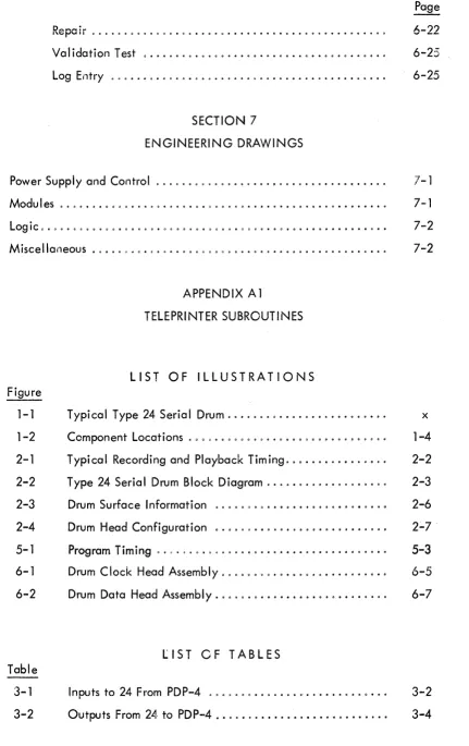
Figure 1-1 Typical Type 24 Serial Drum
SECTION L
INTRODUCTiON
The Digital Equipment Corporation (DEC) Type 24 Serial Drum system serves as an auxiliary data storage devi ce for either of the Programmed Data Processors PD p~; or PD P-4 0 Information
in the computer can be stored (written) in the Sedal Drum and re!rieved (read) in the blocks or 256 computer words 0 After programmed Hnitia~izcrrBonu 256~word blocks of data are transferred
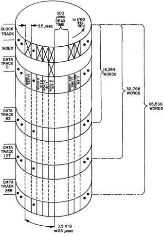
between the computer and the Serial Dr\Jm o~tomaHcal!y; transfer of each word being inter-leaved with the running computer program 0 Serio' Drums are equipped to store either 64, 128u
or 256 data blocks! providing a memorry capabnHy of ]6384u 3276817 or 65536 computer words.
Each word is transferred between the computer and the Serial Drum in parallel (18 bits at a time) and is written or read on the drum surface in series (one bit at a Hme) &
Since application of the Serial Drum is more common ~n a PDP-4 computing system than in a PDP-l system, this manual and the engineering dnaw~ngs assume the machine is connected to a PD P-4. When the Sed es Drum is connected to another computer! a II references in th!s manua I to signal origins and destinations and to data Dnterrupt functions in the PDP-4 can be interpreted to refer to circuits performing similar functions 0
FUNCTiONAL DESCRiPTiON
The basic functions of the Type 24 SerDal Drum are data storage and retrieval17 core memory
address control fl track se!ection17 data request and transfer control i error checkingg and power
supply and distribution. Functional operation of the machfine is initiated by receipt of lOT pulses from the computer. Two computer instructions produce an of the 101' pulses required to enact a 256-word transfer between the COMputer and the Serna I Drum 0
In response to an lOT pulse the Serial Drum requests that the computer enter a data break to transfer a block of information. Eighteen-bit computer words are transferred to the Type 24 one word at a time and are written around the drum one bit at a time when the lOT pulse in-dicates a data in direction ~ Information bits are sensed on the drum one bit at a timet and transferred to the computer one word at a time when the lOT pulses indicate a data in direction ef transfer. During a write cycle a parity bit is generated for each word received from the cemputer; so. that 19-bit werds are written on the drum surface 0 In reading data from the drum
the parity of the word is checked to assure proper transmission. Error circuits in the machine check for parity error during read cycles and check data transmission timing during both read and write eye les. If bits are picked up or dropped out, if data received from the computer is late during a write cycle, er if data is late in being stored in the core memory during a w.rite cycle, an error signal is sent to the computer.
Befere transfers occur, the initial computer core memory address to send or receive data is set into' a register in the Serial Drum 0 This register is automatically incremented by one at the
end ef each werd transfer. Transfers of each block of 256 words is performed at ene track, or address, in the drum. The track address is also transferred to the Serial Drum from the computer befere transfer ef the first word. At the completion of the transfer of the last werd in a bleck this register is automatically incremented by one to simplify the programming ef centinueus block transfers en censecutive tracks 0
Centrel circuits within the Serial Drum request the computer break cycle fer each werd trans-ferred, indicate the cempletien of a block transfer by means ef a flag t signal the detectien er an errer and the direction of the block transfer fJ in additien to' perferming the nermal internal
centrel eperatiens.
PHYSICAL DESCRIPTION
The machine is censtructed ef a DEC computer cabinet 21 5/8 inches wide, 25 3/4 inches deep, and 67 7/16 inches high 0 All indicaters are lecated en a panel at the frent ef the
ma-chine. Maintenance centrels are lecated on the plenum deor inside the deuble rear deers. Pewer and signal cables enter the cabinet through a pert in the bettem. The pewer cable is permanently wired to' the equipment and the two. signal cables mate with cennecters which are mounted on the front of the cabinet, facing the center of the machine 0 Four casters allow
mobility of the machine which weighs 500 pounds with a 16384 or 32768-word memoryu and
t:.t:.n __ •• _-'_ ••• :"L. .... .t..&:.&:.').t.._ ... ~-' _ _ _ ...
~~v fJVUi lu~ vv I i i i U V..J..JvV-VVVI U i!lel/IV! y 0
The cabinet is constructed of a welded steel frame covered with sheet steel. Double front and rear doors are held closed by magnetic latcheso
A
full-width plenum door provides mounting for the power control, power supply u and switch pane! inside the double rear doors 0 Theple-num door is latched by a spring-loaded pin at the top. The indicator panelu racks of logic;
and cable connector panel is attached to the front of a cabinet 0 Module racks are mounted
on the front of the cabinet with the wiring side outwards/1 so that modules are accessible by opening the plenum door 0
A
fan mounted at the bottom of the cabinet draws cooling air througha dust fi Iter in the bottom.v passes it over the electronnc components, and exhausts it through openings in the cabinet 0 The memory drum housing is permanently mounted on braces above
th e fan assemb
I
y .A coordinant system is used to locate racksu modu les and cable connectorsg and terminals!, Each
5
1/4 inch position on the front of the cabinet is assigned a capital letter, beginning withA
at the top, as indicated on Figure 1-2. Modules are numbered from1
through 25 fromleft to right in a rack, as viewed from the wiring side. Connectors are numbered from 1 through 6, from left to right as viewed from the front of the machine. Blank module and connector
locations are numbered. Terminals on a module connector are designated by capital letters from top to bottom. Therefore, D09E is in the fourth location from the top(D)u the ninth mod-ule from the left (09), and the fifth (E) terminal from the top of the module. Components mounted on the plenum
do
0 ra r e. n.o t identHied by location 0 Engineering drawing E-10208shows the system for locating terminal blocks and standoffs mounted on the logic racks 0 The
location of printed-wiring boards in the memory drum housing is indicated on engineering drawing 0-24619.
INDICATOR PANEL
BLANK TYPE 813
POWER CONTROL
LOGIC 1 C
LOGIC 1 D
TYPE 728 POWER SUPPLY LOGIC IE
SWITCH PANEL
PLUG PANEL
BLANK BLANK
BLANK
BLANK
I
I
!
BLANK , I , IFRONT VIEW BACK VIEW
Figure 1-2 Component Locations
[image:15.613.65.253.47.662.2]Dimensions:
Service Clearances:
Weight:
Power Required:
Power D issi pat ion: Power Control Point: Initial Starting Delay: Signal Cables:
Temperature:
Drum Motor:
Magnetic Head Interference:
Write Current:
Pulse Repetition Rate: Word Transfer Time:
Block Transfer Cycle:
(l drum revolution)
SPECIFICATIONS
23 1/2 inches wideg 27 1/16 inches deep, 69 1/8 inches high
8 3/4 inches in front 14 7/8 inches in back
500 pounds for 168384- and
32,768-word memory
550 pounds for 65, 536-word memory 115 volts/ 60 cyc les, single phase, 8-ampere starting current, 5-amperes runn ing current
450 watts
Loco I or remote (computer)
10 minutes
Two, 50 wire, shielded
32 to 105 degrees F operating range 4 degrees F/minute maximum rate of change
20 degrees F maximum allowable instan-taneous change
115 volts, single phase, 2 pole, induction, capac itor start and run
Maximum interchannel read cross talk at least 25 db below nominal signal leveL Maximum noise in any channel at least 25 db below nominal signal level. 80 mill iamperes
305 microseconds 6605 microseconds
17.3 millisecond
ABBREVIATIONS
The following abbreviations are used throughout this manual and on engineering drawings. AC
ACB
Accumu lator in computer
Buffered outputs of Accumulator in computer
ACT
AMP
AMPH
ANS
B
CaMP
COND--DCl
OCT
DOC
DE
OF and DFB
DIC
DNG
- OS
DSB
DT and DTR
DTD
EXT
F
lOS
lOT
MA and MAR
MB
PA
PAR
PC
ABREVIAT IONS (continued)
Active
Amplifier
Amphenol connector
Answered
Break (computer state)
Complement
Conditioned or enabled
Drum Core Location Counter in Serial Drum
Drum Control element in Serial Drum
Drum Data Channel in Serial Drum
Data error
Drum Final Buffer in Serial Drum
Data Interrupt Control in computer
Data No Good flip-flop
Device Selector in computer
Drum Serial Buffer in Serial Drum
Drum Track Address Register in Serial Drum
Drum Track Address Decoder in Serio I Drum
External
As a subscript means final or last bit of information; the bit after the least
signi-ficant data word bit ~
Wnpuf. Oui-pu" II a I C Sk:I t ' I n :,...,..-:1 "--t"",, II I :"Y : ... a ' 1 . '" "'omn,·tet" I...,"" •
Input Output Transfer
Memory Address Register in computer
Memory Buffer Register in computer
Pu Ise ampl ifier
Parity
Power Control (Type 813)
PE
PG
PIC
R
RD/WR RQ
R/wp
S
SA
TRA
WD
XA
XB
YA
YB
ABREVIATIONS (continued) Parity error Pulse generator
Program Interrupt Control in computer Read
Read/Write flip-flop Request flip-flop
Read/Write Parity element in Serial Drum As a subscript means the first or initial bit of information; the bit preceding the most significant data word bit.
Sense amplifier Transfer
Write Data flip-flop
Most significant octal digit of X address Least significant octal digit of X address Most significant octal digit of Yaddress Least significant octal digit of Yaddress
SECTION 2
PRINCIPLES OF OPERATION
RECORDING AND PLAYBACK TECHNIQUE
The Type 24 Serial Drum utilizes Manchester non-return-to-zero (NRZ) or phase modulation recording to enhance the operating margins at the high densities used. This recording tech-nique produces playback head voltages which are either fully positive or fully negative at
read strobe time. Therefore the effective playback signal is twice the ampl itude of that pro-duced by other recording methods in which the sense ampl ifier must discriminate between the presence or absence of uni-directional flux. Data and signal patterns produced in recording and playback of information in the Serial Drum are indicated in Figure 2-1.
BLOCK DIAGRAM DISCUSSION
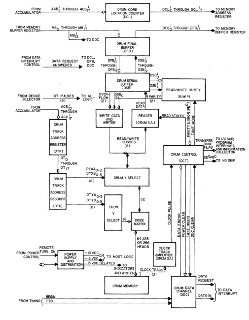
Major functional elements of the Serial Drum are shown in Figure 2-2. Complete information transfer flow and timing of operations in the Serial Drum are indicated in engineering drawings 0-24611 and C-24612.
Drum Core location Counter (DCl)
The DeL is shown on engineering drawing D-24604 to be a 16-bit flip-flop register which con-tains the computer core memory address to or from which the next word is to be transferred. Before tr<;msfer of the initial word in a block, the address of the first word is set i"nto the DCl from the computer accumulator. As each word is transferred the DCl is automatically incre-mented by one.
Drum Track Address Register (DTR)
The DTR is an 8-bit fl ip-flop register which contains the address of the drum track selected for transfer o~ a data block. The drum track (which may be considered as the data block address in the drum or as the address of the selected drum head) is set into the Serial Drum, during program initialization! from the accumulator of the computer. At the completion of a success-ful block transfer (if the DE
O
'
PEa flag is a0)
the DTR is incremented by one to simplifyCI
<t
w
a::
TIME IN MICROSECONDS
DSBo (Example of word to be written)
WRITE DATA FLIP-FLOP
HEAD CURRENT
DRUM SURFACE FLUX
HEAD VOL TAGE (Input to Sense Amplifier at terminals F and H) AND SENSE AMPLIFIER SLICE LEVEL (terminal S)
READ STROBE
SENSE AMPLIFIER LEVEL (terminal M)
SENSE AMPLIFIER OUTPUT
L
(t erminal L) DSBs7 14 21
I I I I I I I I I I I I I I I I I I I I I I I I 28
rAM TRANSFER
_ _ ---oJ 0
I
1 ':1 0 o oL
fCOMPLEMENT
~'---il
,
10=
l-'=II
~ILJI
+1 SATURATE
:-=\
~
/ \
/ l
L
O~ ~~~
- I SATURATE '
-+ 0 SATURATE
~ ~
/ \ / \
/ \ (
c=J
c=J~V-0 SATURATE
- t
--t
-f
f----~t---Figure 2-1 Typical Recording and Playback Timing
[image:21.612.102.531.54.706.2]FROM ACB~ THROUGH ACB I~ __
ACCUMUlATOrn~---~---~~---<~~ lOCATION COUNTER DRUM CORE
(DCl)
DCL~ THROUGH DCL 117 ~ TO MEMORY
~---:---~----~~~~ADDRESS
REGISTER
I I
FROM MEMORY MBa THROUGH MB 17
BUFFER REGISTER~---...!01.----'---.!..!.---'l r---"'---'-'---.~ DFB6 THROUGH DFB 117 . - TO MEMORY BUFFER REGISTER
FROM DATA INTERRUPT CONTROL
l
MBI~ ()- -... ~ .. TODDC
TO DCl.
DATA REQUEST DFB.
ANSWERED. DOC
DRUM FINAL BUFFER "" (DFB)
DFB6 ~ DSB6
THROUGH THROUGH
DFBI~O DSBI~
~~~---~DSBb
~---~
DRUM SERIAL
BUFFER !""";G DSB'
H
{ DSB)
READ/WRITE PARITY
~~---~~
FROM DEVICE lOT PULSES ~ TO ALL OVER- DSBO ~~ PARITY (R/W P)
SELECTOR (5) r ' LOGIC F(L
20)W (2)'r---IC:;}"4 READ (2) _ _ ...:.~~--.._..J o~ ~~
FROM ACB Ib ~ • OAT A -~
ACCUMULATOR'---... THROUGH
i
I WRITE DATA READER ~READ STROBE ~ ~
ACB I7 AND ' a:: Q
WRITER (DRUM SA) W 3;
<t ~~ a::<{
~I-DRUM TRACK ADDRESS REGISTER (DTR) READ/WRITE BUSSES (2)
TRANSFER TO I/O SKIp,
() PROGRAM
~~
DTO THROUGH
DTI7 DTXAO_3
DTXBO_~
(8) .... DRUM X SELECT
DRUM
TRACK
ADDRESS
DECODER
(DTD)
DTYAO_3 r---"'"
DTYBO_~ 32
REMOTE FROM POWER TURN Ott.
CONTROL ..
(8) ". DRUM
<
Y
SELECT ~ DIODE
MATRIX
<.
64,128
OR 256
HEADS
SUPPLY -J5 VDC":' TO MOST LOGIC
POWER + 10 VDC ...
i
AND ...
. - -_ _ _ _ _ .L-l'--' _ _ ... DONE INTERRUPT.
FLA~ND INFORMATION r---COLlECTOR
DRUM CONTROL DEQp~
(OCT) r--+TO I/O SKIP
~""lI~~r---<r-}~-r-lIAr-~-W CI) ...J ::> a. ~ u o ...J U CLOCK TRACK AMPLIFIER
(DRUM SA)
~---t~.. DISTRIBUTION - 15 VDC 0 LAYED;; TO
INDICATORS CLOCK TRACK'
AND WRITE~t J (2) DRUM MEMORY
_ ... _" .... 'n ... '..., DATA REQUEST
DRUM DATA CHANNEL
(DOC)
BEGIN ..
FROM TIMING{-1...T7..!..2B~ ______________________________________ ... ~
~}TO
DATA [image:22.618.51.557.41.692.2]DATAI~ INTERRUPT
...
_---Figure 2-2 Type "24 Serial Drum Block Diagram
,
,
programming of C(IlI'i-inuous transfers at successive drum tracks, Engineering drawing 0-24607
shows the OT R.
Half of the drum track selection is performed by decoding of the OTR flip-flop outputs in the
DTD. As shown on engineering drawing 0-24607 Q the DTD consists of two groups of eight
2-input diode gates, one group for the X address and one for the Y address 0 The eight X address
outputs function as a two-digit octal address which is further decoded in the Drum X Select
logic 0 The eight Y address outputs serve a sim ilar function 0
Drum Head Selection
Final selection of a drum head is performed in the Drum X and Y Select circuits shown on
en-gineering drawing E-24608 and in the diode matrix within the drum housing. The 16 FIELD
LOCKOUT switches each inhibit a Type 4521 Drum X Select Module when closed and so
pre-vent accidental writing in 16 addresses 0
Drum Sense Ampl ifiers
Two Type 1537 Drum Sense Amplifier modules convert information sensed
by
the magnetic headsof the drum into digital pulse data. Information recorded on a clock track is sensed
by
theclock head and supplied to the sense amplifier shown on drawing D-24603 as the Clock Track
Amplifier. The output from this sense amplifier is applied to the Drum Control (DCT) to
estab-lesh the basic clock rate of all drum operations. The sense amplifier shown on drawing 0-24602
as the Reader samples the signals picked up
by
the selected data head and produces a puLse toset a
1
into the Drum Serial Buffer (DSB) when the read strobe signal occurs during the maximumnegative excursion of the head signal.
Drum Control (OCT)
The basic timing pulses for the machine are generated in the OCT from pulses received from
the Clock Track Amplifier 0 The DCT also contains a 4-state device consisting of four negative
diode gateso Each state of this device corresponds with and initiates one of the four machine
control states: idleu transfer, activeu or transfer done 0 This logic is shown on engineering
drawing 0-24603.
Drum Data Control (ODC)
Engineering drawing D-24605 shows the DDC 0 Circuits within the DDC control the transfer of
each word between the computer and the Drum Serial Buffer 0 The DDC establishes the read/
write status of the machineq makes the data break request for a computer break cycleq indicates
the detection of an errorq and designates the direction of the ensuing data transfero
Drum Final Buffer (D.FB)
The DFB is an l8-bit register which serves as a buffer between the computer Memory Buffer Register and the Drum Serial Buffer 0 Words are transferred in parallel (18 bits at a time) under
control of the computer Data Interrupt Control 0 During the drum writ'lngu DFB holds the next
word. During drum reading, DFB is empty and is prepared to accept information read from the DSB and place it into core memory under control of the Data Interrupt Control 0 The logic
cir-cuits which compose the DFB are shown on engineering drawong D-24606 0
Drum Serial Buffer (DSB)
As shown on the top and left side of engineering drawing D-24602, the DSB is an l8-bit shift register which is a serial-to-parallel-converter during drum reading/1 and a para!!el-to-serial-converter during drum writing 0 Information is read from the drum into DSB serially and
trans-ferred to DFB in parallel. During drum writingq a word is read from DFB into DSB and written
serially around the drum.
Read/Write Parity (R/WP)
As each bit of a word is written on the surface of the drumi the R Parity fiip~flop counts the number of binary 1s and produces a 19 bit to provide an odd parityo When data is read from the drum this flip-flop counts the 1s again and sets the Parity Error flip-flop if an even number is detected in anyone word 0 The condition of the Parity Error
fi
ip-f!op is ind. cated in theDCT as one of the two possible causes of an error condition. These circuits are shown in area C4 and C5 of engineering drawing D-24602.
Write Data and Writer
DATA TRACK
o
3.5 X 19
~66)Jsec
16,384 WORDS
32,168 WORDS
Figure 2-3 Drum Surface Information
65,536 WORDS
contents of the most significant bit of the OSB. This logic is shown in the lower right corner of engineering drawing 0-24602.
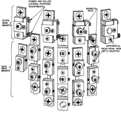
[image:25.615.137.472.54.539.2]CLOCK HEAD MOUNTS
DATA HEAD MOUNTS
r
PUSHER AND PUllER (lATERAL POSITION) ADJUSTMENTS
. . ...
I~
Figure 2-4 Drum Head Configuration
Drum Memory
DIFFER TlAl (HEAD-DRUM
PROX-IMITY) ADJUSTED
The rotating drum assembly is designed with minimum cross-section for proper heat transfer and dissipation. It is mounted on separable inner-ring angular-contact bearings which are pre-lubricated for life. Preloading is accomplished b~1 springs at the top end of the unit. The magnetic coating on the surface of the drurY, ~s ' GRIMACOII # 6037-X high density
dis----=--
L. ... _~ __ ... ,J ... ,J 1 ... "'9'" f-", if-c tin,,1 tinichtJ~::a;:)lUII, IICUI-"'UICU ... "'" ... t"t" ... _ ... . Dynamic rlJnOlJt is less than 0.0001 inch
total indicator reading.
[image:26.620.77.552.48.499.2]The motor which turns the drum is of special design to provide the fastest starting time com~
patible with minimum power input and losses at synchronous speed e The fan for this single-phase" two-pale, inductioni capacitor-start and run motor is fastened to the bottom of the spindle. Ambient air is drawn through a shroud and over the finned motor housing 0 This air current takes away heat from the motor preventing local ized temperature rise.
Four panels allow ready access to the drum without disassembly of signai or power connectors. Thus, adjustments of spacing or clock bit al ignment can be made under operating conditions 0
The drum housing is designed so that the fan action of the drum circulates air around the drum and head mounts so that the temperature dHferentiai is kept to a minimum within the housing 0
This internal circulation, together with the external discharge from the motor fang also tends to maintain a minimum differentia~ from inside to outside so that repeated stops and starts can be made without endangering head contact 0 Actual
I
imits of ambient temperatures should bemaintained to 55° Fahrenheit and 115° Fahrenheit with a rate of change not to exceed 15°
Fahrenheit per hour.
The location of tracks and words on the drum are indicated schematically in Figure
2-3
and the relative position of head mounts and the major components of the mounts are shown in Figure2-4.
Power Suppiy and Distribution
The Serial Drum operates fron a single source of 1 15-voit , 60-cycle, single-phase power 0
Control and overload protection of this power w!thin the machine is exercised by a Type 813
Power Control. Operation of the power control can be controlled by the MAINT ON/OFF switch on the switch panel or by means of a contact closure provided by the computer. The ac output of the power control operates the drum motor, fan motor, and the Type 728 Power Supply. The -15 volt output of this supply which operates the indicator panei is controlled
by
a 10 minute time delay relay in the power control 0 Therefore the indicators do not light until
ten minutes after the drum motor has been energizedi at which time the drum has reached
synchronous speed and is ready to transfer data 0
The Type 728 Power Supply produces the normal module operating voltages of +10 vdc and -15 vdc. These outputs are connected to each rack of logic through a color-coded connector
---' a "oggle s'w:"ch a" "l...e .,: .... l..." s:-'e ,..,c e"'-l... "''''eIK as seen ,c"" ... ~h8 ... "'...1,.1 8 s;,..Ie
I\A~"g;nal-UIIU I I !I I ! II! !I~I!I 1\,,1 VI \,,1,-, •• 1\,,1 (} I I b V , I I ' " .11"''''' .... ' , ... , • in .... " •
check terminals are provided on these connectors which are connected in common to all racks,
so that an externa I power supply can be connected to any connector to rna rgina I check a II racks.
The color coding of these connectors is as follows; from top to bottom:
a. Green, + 10 vdc marginal-check supply b. Red, + 10 vdc internal supply
c. Black, ground
d. Blue, -15 vdc internal supply
e. Yellow, -15 vdc marginal-check supply
Three single-pole double-throw switches at the end of each rack of logic allow selection of either the normal internal power supply or the external marginal-check power supply for dis-tribution to the logic. The top switch selects the +10 volt supply routed to terminal A of all modules in that rack. In the down position the fixed internal +10 volt supply connected to the red terminal is supplied to the modules, and in the up position the marginal-check voltage supplied to the green terminal is supplied to terminal A of the modules. The center switch performs the same selection as the top switch for connection of a nominal +10 volt level to terminal B of all modules. The bottom switch selects the -15 volt supply to be routed to ter-minal C of all modules. In the down position the fixed";'15-volt output of the internal power supply, received at the blue terminal, is suppl ied to the modules whi Ie in the up position the marginal-check voltagel connected to the yellow terminal, is supplied to terminal C of all modules.
WRITE CYCLE
Two lOT commands write a block of 256-words on a drum track. lOT 706046 dears the Drum Core Location Counter and clears the Drum Final Buffer. It then loads the Drum Core Location Counter with the contents of AC
2_17, the computer Information Distributor. This information '~ indicates the core memory address of the first word to be transferred. The Read-Write flip-flop
Buffer Register is transferred to the Drum Final Buffer. When the request is made the Data No Good (DNG) flip-flop is set to a 1 and the Data Request Answered signal clears this flip-flop.
"'~-If another request is initiated before the DNG fiip~flop is cleared, signifying that incorrec!t information is in the Drum Fina I Buffer Ii' a Data Error (DE) resu Its.
~
The second lOT 706106 clears the Drum Track Address Register and the error flip-flops at time
pulse 7, and then loads the track address into the DTR at time pulse 1 of the next cycle._ A ,", I'
N. -. - - ---_ .~r, r,t,
,~_~'."1puter break cycle is initiated to bring the first word to be written from the DFB to the DSB and loads DS~ unconditionally with a binary 1 and brings the second word to be written from core memory into the DFB ~ After a delay of 200 microseconds the transfer request (TRA) state is set. This delay allows the track selection capacitor-diode gates to set up. After a period -of O.to 17 milliseconds (up to one drum revolution time) the clock track initiates the first timing
",- :,_, __ .. r - ~ .Z -(,. l_.~
pu Ise and the system timing passes to the drum, At the ¢B clock time the DSB is shifted, bring-ing the next bit to be written into the DSB
O fl ip-flop and bringing a 0 into the DSBS. At this time the bit arriving in the DSB
O is jammed into the Write Data fl ip-flop. At the ¢ A time the Write Data flip-flop is complimented, creating the proper flux transition on the drum
sur-, ' , . ; , \ ) ' . ; ( ) f['.} ," ~I •
face. After 18 bits have been written all zeros
wil(~xist
in the DSB'and a 17-input AND gate wi II detect this condition and create an overflow. As each of the 18 bits is written the R Parity flip-flop is complimented for each 1 recorded. Since this flip-flop was originally set to 1, after the 18th bit is written it contains the proper odd parity bit 0 When the overflowoccurs the state of this fl ip-flop is jammed into the Write Data fl ip-flop and is recorded as the odd parity bit.
After the parity bit is recorded a data request is made to the computer 0 The present contents
of the DFB are read into the DSB and the next word to be written is brought into the DFB via a request to the computer 0 After 256 words are writtenl a flag is sensed in the Program Inter-rupt and the decision to continue writing the next block, or to initialize a new core memory location and track address, or to halt I is made by the program 0 A continue instruction writes the next block of 256 words 0 This instruction may be given any time during the 300 microsecond
READ CYCLE
Two lOT commands read a biock of 256 words. lOT 706006 dears the Drum Core Location Counter, clears the Drum Final Buffer and loads the Drum Core location Counter from the In-formation Distributor (AC
2_17) with the core memory address into which the first word wi
II
be read from the drum. The Read/Write flip-flop is set to the read status and produces the Data In signal which is suppl ied to the computer. This signal inhibits generation of the core read strobe pulse so that the Memory Buffer Register remains cleared and allows insertion of new data. lOT 706106 clears the Drum Track Adqress Register at T7 time and loads the new track address, from which information is to be read, at the next cycle. A binary 1 is unconditionallyloaded into DSB
17 and 200 microseconds later a transfer request state (TRA) is set. When the first timing mark on the drum occurs the transfer commences. Bit one is read into DSB
S. For each 1 that is read the R Parity flip-flop, which was originally set to 1, is complimented. After reading nineteen bits and shifting the information through the DSB, DSB
17 arrives at DSB
F and an overflow condition is created. This overflow initiates a Take Word signal which transfers the assembled word in the DSB into the DFB. It creates a data request condition in the computer so that the Memory Buffer Register takes the word in DFB and inserts it in core memory at the address specified by the DCl. This Take Word signal tests the state of the R Parity flip-flop. Since R Parity was originally set to
1
i and each1
that was read into DSBcompl iments R Parity f then at the end of 19 bits (18 bits plus the parity bit) the R Parity
flip-flop must contain a 0 if the parity was correct during writing and the correct number of
1s
and Os were read. If R Parity is a1
at Take Word time a parity error wiII
resuIt.
The computer has 66 microseconds in which to take the word which exists in the DFB and insert it in core memory, 'so that the DFB may be cleared and ready to receive the next word from DSB. At the end of a 256-word transfer the drum transfer done flag is set to 1 and creates a program interrupt. The programmer now has the option of giving a continue instruction to bring the next successive block of 256 words into core memory, initial izing a new core memory location and track address, or terminating the transmission.SECTION 3
INTERFACE
All logic signals which pass between the computer and the Serial Drum are standard DEC levels or standard DEC pulses. A standard DEC level is either ground potential (0.0 to -0.3 volts) or -3 volts (-3.0 to -4.0 volts). Standard DEC pulses are 2.5 volts in amplitude (2.3 to 3.0 volts) and are 0.4 microsecond in duration. Positive pulses are referenced to the standard negative
level and negative pulses are referenced to ground potential.
Throughout the manual standard DEC ground-potential signals are symbol ized by an open dia-mond and standard DEC negative levels are indicated by a sol id diadia-mond. Open and sol id ar-row heads are used to symbolize standard DEC positive and negative pulses,:' respectively. In addition to the logic signal inputs a contact closure in the computer power control circuit provides the remote turn on signal to the power supply and distribution network in the Serial Drum. This signal is used to energize or de-energize the Serial Drum from the computer in normal operation. The effect of this signal can be disabled during maintenance ,operations to control power application and removal via a switch on the Serial Drum.
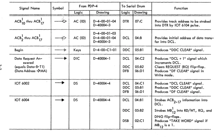
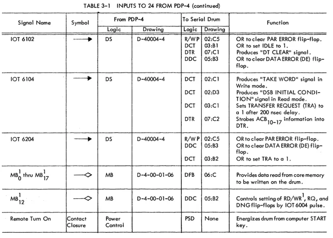
Input signals to the Serial Drum are listed in Table 3-1 and output signals are listed in Table 3-2. Numbers in the Serial Drum Drawing column of these tables indicate the engineering drawing number when prefixed by D-246. The letter and number following the colon indicates the horizontal and vertical coordinates on the engineering drawing where the signal can be found. Signal origins in Table 3-1 and signal destinations in Table 3-2 are given for inter-face with a PDP-4 computer. When planning interinter-face between the Serial Drum and another computer these tables can be used as a guide for connection to circuit elements performing similar functions.
Note that input signal levels to the DCl, DFB, DTR, and DDC must be present for at least 3 microseconds before receipt of the lOT pu Ise or T7B pu Ise wh ich strobes the data contents into the flip-flops. This delay is required to allow settling of the capacitor-diode gate at the in-put of each fl ip-flop.
TABLE 3-1 INPUTS TO 24 FROM POP-4
-Signal Name Symbol From POP-4 To Seria I Drum Function
logic Drawing logic Drawing
-1 1 .::: .. i
AC (10) 0-4-00-01-04 07:C Provides track address to be strobed ACB
10 thru ACB17
----<>
I I OTR0-40004-3 into OTR by lOT 6104 pu Ise.
I
I
0-4-00-01-031 1
---{(;>
I
ACB
2 thru ACB 17 .', I AC (10) 0-4-00-01-04 OCl O4:B Provides initial address of data tran
0-40004-3 fer into OCl e
s-
.-Begin
1>
Keyso
-4-00-C 1-01 DOC 05:B1 Produces IIOOC ClEAR" signal 0
-Data Request An-
Ii>
DIC 0-40004-1 DCl 04:C2 Produces "DCl + 1" signal whichswered increments DClo
(equals Data-B"T1) DOC 05:B2 Clears REQUEST (RQ) flip-flop.
(Data Address
=>
MA) DFB 06:01 Produces IIDF ClEARIl signal inWrite mode.
-lOT 6002
--.
OS 0-40004-4 DCl O4:Cl Produces "OCl ClEARIl signal.DOC 05:B1 Produces IIDOC CLEAR" signal. DFB 06:01 Produces IIOF ClEARIl signal.
-lOT 6004
--.
OS 0-40004-4 DCl 04:B1 Strobes ACB2_17 information into DCl.
DOC 05:B2 Strobes
MB~2
into RD/WT I RQJ' an dDNG flip-flops.
DSB 02:C1 Produces "TAKE WORD" signal if
. ,
MB12 is a 1 .
.
[image:33.793.52.753.66.513.2]-W
I
W
Signal Name
()T 6102
()T 6104
()T 6204
1
1"BO thru MB 17
1 "B 12 .
R
,emote Turn OnTABLE 3-1 INPUTS TO 24 FROM POP-4 (continued)
Symbol From 'POP-4 To Seria I Drum
Logic Drawing Logic Drawing
...
OS 0-40004-4 R/WP 02:C5OCT 03:81
OTR 07:Cl
DOC 05:83
•
OS 0-40004-4 OCT 02:C1OCT 02:03
OCT 03~Cl
OTR 07~C2
..-
OS 0-40004-4 R/WP 02:C5DOC 05:B3
OCT 03:B2
- - 0
MB 0-4-00-01-06 OFB O6:C----<>
MB 0-4-00-01-06 DOC 05:B2Contact Power PSO None
Closure Control
Function
OR to clear PAR ERROR flip-fl Ope
OR to set IDLE to 1.
Produces "OT CLEAR" signal.
OR to clear OAT A ERROR (DE) i·
"lip-flop .
Produces "TAKE WORD" signa
I
inWrite mode.
Produces "OSB INITIAL CON[
)1-TION" signal in Read moden
Sets TRANSFER REQUEST (TRA ) to
a 1 after 200 nsec delay 0
Strobes ACB
10_17 information
OTR.
into
OR to clear PAR ERROR flip-flo
p.
ip-OR to clear DATA ERRip-OR (DE) fl
flop.
OR to set TRA to a
1.
Provides data read from core mel to be written on the drum.
Controls setting of RO/WR 1, R( ONGflip-flops by lOT 6004 pi
mory
~, and ulse.
[image:34.794.62.740.66.551.2]TABLE 3-1 INPUTS TO 24 FROM PDP-4 (continued)
-Signal Name S ymbol From PDP-4 To Serial Drum Function
====1===
logic Drawing logic DrawingT7B
..
Timing 0-4-00-01-01 DOC 05:03 Produces a "T7C" pu Ise after 1 nsec which clears the DFB in the Read mode, increments the DFB in the Writ emode, and clears the DATA NO GOOD (DNG) flip-flop in the DOC"
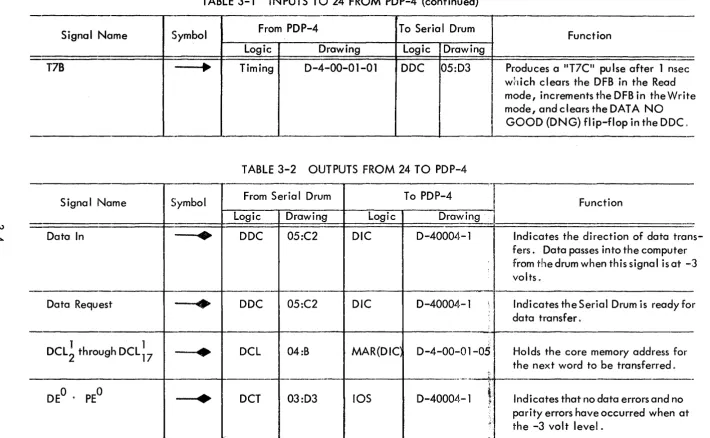
TABLE 3-2 OUTPUTS FROM 24 TO PDP-4
.--,
Signal Name Symbol From Serial Drum To PDP-4 I Function
.- logic Drawing logic Drawing
I
Data In
•
DOC 05:C2 DIC 0-40004-1 Indicates the direction of data trans-fers. Data passes into the computer from the drum when this signal is at -3
volts.
-
-Da ta Requ es t
..
DOC 05:C2 DIC 0-40004-1 Indicates the Serial Drum is ready fo rdata transfer .
.
-1 1
DCl 04:8 MAR(DIC~ 0-4-00-01-05 Holds the core memory address for DCl
2 through DCl 17
•
the next word to be transferred 0
"
.- ----..
-r
DEO . PEO
•
OCT 03:03 lOS 0-40004-1i
Indicates that no data errors and no parity errors have occurred when at~.
the -3 volt level.
[image:35.794.49.759.65.503.2]Signal Name
1 1
DFBO through DFB 17
T ransfer Done Flag
~~--TABLE 3~2 OUTPUTS FROM 24 TO PDP-4 (continued) !
i
I
Symbol I From Serial DrumI
I
Logic Drawingt
-.
..
I
DFB 02:B•
OCT 03~A4!
I
~ t
f
,
-~J---~-~-L-. --~
Logic
MB (Ole)
lOS
PIC
-.-.-~~.
ToPDP-4
J
FunctionDrawing
I
~
D-4-00-01~06 ~
D-4004-1---1
I
!IProvides data read from dru m which moryo is to be writf'en in core me Signals completion of a bio fer when reverting to ~3 vo
ck
trans-l"ts (Nomi-nally ground level) 0
[image:36.794.68.758.76.235.2]SECTION 4
INSTALLATION AND OPERATION
SITE REQUIREMENTS
The installation site must provide floor space at least 14 inches wide and 28 inches deep to accomodate the Serial Drum. At least 9 inches must be provided in front of the cabinet and
15 inches at the back of the cabinet to allow opening of the doors for maintenance.
A source of 115-volts (±17 volts), 60 cycle, single-phase power must be supplied by the site.
Th!s ·o··rce must be -a-able I II :> U ~ jJ' I 0' I su-ply'ing jJ' I ,-L._ I I i C 8 " am---- "'-a-'-:ng s' ... _- _. · .... en" -nd .v= " ! - " C I C ; ) I I I I I VI~C '"'VII ... ..,.V-"'II l:;: n -mpe"e •
running current required by the Serial Drum.
Ambient temperature at the installation site can vary between 32 and 105 degrees Fahrenheit (0 to 41 degrees Centigrade) without deleterious affect upon equipment operation. For normal operation an ambient temperature range from 70 to 85 degrees Fahrenheit is recommended. Note that rapid changes in temperature adversely affect the operation of the drum memory only when the covers are removed. Therefore, the installation site should be capable of maintaining a relatively stable temperature during drum maintenance, such as during the drum head spacing checks.
SIGNAL AND POWER CONNECTIONS
All signal connections to the Type 24 Serial Drum are made at connectors F 1 and F2 on the plug panel at the front of the machine. To mate with these connectors, a cable should con-tain an Amphenol connector of the 115-114P series with a housing 1391 and wire clamp 3057. Maximum signal cable length should not exceed 25 feet. The input and output signals are de-fined in Tables 3-1 and 3-2 and their wiring connections are given on sheets 1 and 2 of the en-gineering drawing A-24614.
A grounded, wire power cable is permanently attached to the machine. A standard three-prong male power plug at the end of this cable allows connection to a power source at least
18 feet from the cabinet.
CONTROLS AND INDICATORS
All manual control of the Serial Drum is exercised by means of toggle switches on the switch panel at the rear of the machine. The function of these switches is as follows:
MAINT ON / OFF
REMOTE ON/OFF/LOCAL ON
FIELD LOCKOUT
(0 through 7 and 10 through 17)
Allows maintenance personnel to select the norma I or stop-on-error mode of opera-tion. In the OFF position the equipment functions normally and data errors or
par-i ty errors can be detected via the error flag only at the end of a 256-word block.
In the ON position detection of data error or parity error by the machine in-hibits generation of clock signals (¢Ai
Read Strobe, and
¢s)
so thatall
data transfer stops and the contents of aII
re-gisters can be observed to locate the cause of the error.Allows local or remote control of machine energization. In the REMOTE ON posi-tion the machine is energized by a con-tact closure in the computer. The OFF and LOCAL ON positions function as a normal power switch.
Each switch allows a group of 16 con-secutive tracks (4096 words) to be inhib-ited during writing so that the information stored on those tracks cannot be acc iden-tally destroyed.
Visual indication of the machine status and register contents is given on the indicator panei. The functions denoted by these lamps are as follows:
TRACK ADDRESS (8)
CORE LOCATION (16)
FINAL BUFFER (18)
SERIAL BUFFER (18)
Light to indicate ONEs in the Drum Track Address Register.
Light to indicate ONEs in the Drum Core Location Counter.
Light to indi cate ON Es in the Drum
Fi-na Buffer.
light to indicate ONEs in the Drum Se-ria
I
Buffer.READY (RD and WR)
(2)
TRA
ACT
FLAG
OVERFLOW
REQUEST
PE
DE
Indicate the machine is in ejther the read or write mode 0 Either of these lamps light
to indicate that the initial delay following energization of the power control has
e-lapsed and the machine is ready for use.
Lights to acknowledge receipt of lOT pu Ises and indicate that the machine has been taken out of the idle state and is waiting for clock pu Ises to be read from the drum to assure that the drum is in the correct position before initiating a transfer 0
Lights to indicate that the machine has been taken out of the transfer state and is actively engaged in a data transfer. Lights to indicate that a block transfer has been completed and the machine has been taken out of the active state 0 The
machine remains in this state until the flag is cleared when the machine is set to either the idle or the transfer state. Lights to indicate that a 19-bit word has been assembled in the DSB and is ready for transfer to the DFB in the read mode, or that a 19- bit word has been transferred from the DSB to the drum in the write mode 0
Lights to findicate that a data request sig-nal has been sent to the computer to re-quest a data break to transfer a word. Lights to indicate that the machine has detected a parity error after read-in from drum to core. If the MAINT ON/OFF switch is OFF when a parity error occursi' the drum error flag is set to 1 i if the switch is ON u the flag is set to 1 and the
trans-fer is terminated,
DE (continued) or when writing the next word to be writ-ten has not been received by the DFB).
If the MAINT ON/OFF switch is OFF when a data error occurs, the drum error flag is set to 1; if the switch is ON I the
flag is set to 1 and the transfer is terminated. This condition occurs either because de-vices with higher priority are connected to the Dahl Interrupt Control, or because the instruction being executed at the time of the data request takes longer than 66 microseconds for completion.
EQUIPMENT TURN-ON AND TURN-OFF
Operation of the Type 24 can be controlled locally by operation of a switch, or' remotely from a signal received from the computer. Control point is selected at the REMOTE ON/OFF/ LOCAL ON switch on the switch panel. In normal use this switch is left in the REMOTE ON position with the circuit breaker in the ON position. For maintenance operations this switch is set to the LOCAL ON position to apply power and to the OFF position to remove power. Power is not controlled by manual operation of the circuit breaker. Note that the circuit breaker must be in the ON position to allow either local or remote control of primary power in the Serial Drum
by
means of the switch; setting the switch to the REMOTE ON position alone is not sufficient for remote operation.SECTiON 5
PROGRAMMING
INSTRUCTION CODES
The functions performed by lOT pulses in the Serial Drum are listed in Table 3-1. Combining these pulses and adding the skip group yields the instruction list given in Table 5-1 .
Octal
Code
706006
706046
706101
706102
706106
706201
706204
TABLE 5-1 TYPE 24 SERIAL DRUM INSTRUCTION LIST
Mnemonic
Code
drlcrd
drlcwr
drsf
drcf
drlblk
drsok
drcont
Operation
load the Drum Core location Counter with the core memory location information in Accumulator bits 2 through 170 Prepare to read one block of information from the drum into the specified core location.
*
load the Drum Core location Counter with the core memory location information in Accumu lator bits 2 through 170 Prepare to write one block of information into the drum from the specified core location.'*
Skip next instruction if the drum transfer done flag is a 10 {The block transfer RS complete.}o
0Clear the drum transfer done fiag and the DE 0 PE
error flag 0
Load the Drum Track Address Register with the con-tents of Accumulator bits 10 through 17. Clear the drum transfer done flagi clear the DEO. PEO error flagg and begin a transfer (reading or writing) 0
*
Skip next instruction if the drum transfer done flag is not a 1.
o
0
Clear the drum transfer done flag! clear the DE . PE error flag and begin a transfer.
*The Drum Core Location Counter is incremented after each word transfer and the Drum Track Address Register is advanced to the next position at the end of each block transfer if the drum error flag is not set to a 1 and the MAINT ON/OFF switch is in the OFF position.
[image:42.615.60.557.237.710.2]PROGRAM TIMING
Two instructions cause the transfer of a 256-word block" The first (drlcrd or drlcwr) specifies the core memory location of the block and the direction of transfer (drum-to-core or core-to-drum)" The second instruction (drlblk) specifies the block or track number and initiates the transfer. Transfer of each word is performed during a data break, under control of the computer Data Interrupt Control, and is interleaved with the running program"
The timing of a block transfer is shown in Figure 5-1. A transfer begins when the continuously rotating drum reaches the index mark, 3 Q 5 microseconds before the beginning of the data track
(word 0, bit 0)" A 300-microsecond interval separates the end of a block from its beginning" Because the selection of a read-write head requires 200 microseconds stabilization time, a new track must be specified during the first 100 microseconds of the 300 microsecond interval for continuous transferring. If selected tracks are consecutive, uninterrupted transferring may be programmed merely by specifying continuation, since the block number is automatica Ily in-cremented at the end of each successful block transfer and core memory location is automatically incremented at the completion of each word transfer" The continuation instruction (drcont) can be given at any time during the 300-microsecond interval.
The drum transfer done flag is set to 1 upon completion of a block transfer, causing
a
program interrupt. The flag is cleared when a drcf instruction is issued specifically for that purpose, or automatically when either tha drblk or drcont transfer instruction is given" The drum transfer done flag is associated with bit 17 of the computer in-out read status instruction"The DE
O
"
PEO
error flag should be checked at completion of a block transfer. If this flag is a 1 it indicates either of the following conditions:(a) A parity error has been detected after read-in from drum to core memory. If the MAINT ON/OFF switch is in the OFF position when a parity error occurs, the error flag in the computer is set to 1; if this switch is in the ON position, the error flag is set to 1 and the transfer is terminated"
(b) The data request signa I from the drum was not answered by the computer within the 66-microsecond period. The data transmission is terminated and the error flag in the computer is set to 1. This condition occurs either because
... he ..
de":c""su,:"'h
I... ";gher p"";or:tv ,.. .. e con ... e,.. ... e,J "'0 ... J,..,,,,,, "'''mpu+c " D"+,, In+e .... "p+V I I I VI c; V Y I Q I I I I ' 1 / \,AI 1111 "". \.AI I~I~"""'" I I v l ... , . . . .
CLOCK TIMING
START/DONE FLIP-FLOP
TRANSFER DONE FLAG
lOT PULSE 706102 (or 706106 or 706204)
rOT PULSE 706106
66ps
~ ~I
I
~ ~3.5}JS Ind •• time ~1111·· ·1
f4..---
300psec - - - -. .111·· ·1111
012 '--v---' 17P 01.2 17POI
l .. J l J l _ _ ... ~_
Word 255
l
lOT 706204 maYn~~tgi~3~iO transfer onI
Latest time instruction may be given to transfer on next index.
"'~I---200)Jsec --~~~I
Figure 5-1 Program Timing
Word 0 Word I
Control, or because an instruction requiring longer than 66 microseconds for
completion was in progress at the time the data request was made.
The programmer should be aware of the settings of the FIELD LOCKOUT switches to avoid
at-tempting to write at track addresses which are inhibited by switches being in the up position.
The octal addresses inhibited by each switch are as follows:
Switch Addresses Switch Addresses
0 0000 to 0017 10 0200 to 0217
1 0020 to 0037 11 0220 to 0237
2 0040 to 0057 12 0240 to 0257
3 0060 to 0077 13 0260 to 0277
4 0100 to 0117 14 0300 to 0317
5 0120 to 0137 15 0320 to 0337
6 0140 to 0157 16 0340 to 0357
7 0160 to 0177 17 0360 to 0377
[image:44.615.89.524.82.400.2]