STANDARD ftICROSYSTEMS
CORPORATION
s=.=:s======
=====:=*== ... ::'11
ARC NET
LOCAL
AREA
NETWORK
CONTROLLER
DESIGNER'S
GUIDE
PUBLICATION
900.C06ATable
oi
Contents
1.0
GENERAL INFORMATION . . • . . . .
1.1 ARCNET-PC FAMILY DESCRIPTION
. . . • . .
1.2
ARCNET FAMIL. Y FEATURES:
• • . . • . . .
2.0
SPECIFICATION3
.
.
. . .
.
.
.
.
.
.
. .
2.1
2.2
2.3
ARCNET-PC FAMIL.Y BLOCK DIAGRAM
2.1.1 ARCNET- PC100. 200, 300
. • .
2.1.2 ARCNET-PCll0, 210, 310:
. • •
PHYSICAL SPECIFICATIONS • • •
TOPOLOGICAL SPECIFICATIONS
• • .
2.3.1 ARCNET-PC 100,110
• • •
~
.
2.3.2 ARCNET-PC 200, 210 •
2.3.3 ARCNET-PC 300, 310 • •
2.3.4 TOPOLOGY EXAMPLE • •
·
. .
3.0
ARCNET-PC SWITCH CONFIGURATION
·
. .
.
.
. .
3.1 SWITCH GROUPS OVERVIEW
· · ·
3.2 SWITCH GROUP _2 SETTINGS
·
·
·
·
· ·
·
·
·
3.2.1 SWITCHES 1
- a
NODE ADDRESS VAL.UE
·
3.3 SWITCH GROUP _1 SETTINGS
·
·
·
· ·
·
· ·
3.3.1 SWITCHES 1
- ·6 1/0ADDRESS VAL.UE
·
·
·
·
· .
.
·
·
·
·
·
·
·
· · ·
·
3.3.2 SWITCHES 7
-
10
RAM SUFFER ADDRESS VALUE
4.0
ARCNET-PC JUMPER CONFIGURATION
S.O
ARCNET-PC REGISTER:5 • • • •
· . .
.
.
.
.
.
.
.
6.0
ARCNET-PC MEMORY
ADORE~SING•
·
. . .
·
.
·
. .
.
.
7.0
THEORY OF OPERATION • •
·
.
.
·
.
.
7.1 Addre •• Decodin9
·
·
·
·
•
·
·
·
•
·
·
·
·
· ·
7.1 Addre •• Decodin9
·
·
·
•
·
·
·
· ·
·
•
· ·
7.2 Int.ern.l Addre •• -D_t._ Sua
·
·
·
7.3 Wa.t.t. St.at._ Gener_t.or
·
·
0 0
· ·
0
7.4 Int.arrupt..
•
.
•
·
·
· ·
· · · ·
0
· · ·
0
70S Cable Tranac:eiver
·
0
·
• •
· ·
•
·
·
•
·
·
1
1 2
3
3 3 3
"
"
"
"
5 5
6 6 IS IS 6 7
7
s
s
s
S
9 9 9 9
10
8.0
PROGRAMMING
CON~IOERATION~• • • . • • • • • • . • • •
10
1.0
GENERAL
INFOR~ATION1.1 ARCNET-PC
FA~ILY OE~CRIPTIONSMC'a ARCNET-PC
i • •ily o£
n.twork controll.r bo.rd. prov1dea the
u •• r with a .iaplifi.d int.rf.c. b.tw •• n
the
IBM
PC
bu.
and an
ARCNET .odifi.d tok.n p ••• ing
~ocalAr •• Network. Th. ARCNET-PC, 1n
addition, provid.. the
co.pl.t. controll.r for
the
local area
network,
which
r •• ult. in
virtually
u •• r
transparent
network
op.ration and control.
The ARCNET loc.l
ar.. n.twork
wa.
origin.lly d.v.lop.d by the
O.tapoint Corporation a. a high p.rfor •• nc. local ar.a n.twork used
to
int.rconn.ct
.ophi.tic.t.d
co.puting
.y.t....
Now
the
p.rfor •• nce capabiliti.. of thi. n.twork . r . avail.bl. to u •• ra of
IBM PC .nd PC
co.patible co.put.r .y.t
•••• The
ARCNET-PC fa.ily
incorporat..
the Standard Micro.y.t • • • •
ingle chip COM 9026
~ocalAre. Network Controll.r .nd COM
9032
ARCNET
Local
Are. N.twork
Tran.c.iv.r
LSI
circuit. to
provide
co.pl.te ARCNET
protocol
h.ndling on • •
ingle
bo.rd. A 2K on-bo.rd
Oat. Packet
Buff.r 1s
u •• d
to
provide
four
p.g.. o£
p.ck.t .tor.ge. Thi.
..y be
dyna.ic.lly u •• r
d.£in.d
to
provide double
bu££.r1ng
for both
tran •• i t and
rec.iv. £unction •• Th.
controll.r •• y b. polled or
interrupt driv.n. An on-board 8K
PROM .ock.t
i • •
v.il.bl. to the
u •• r for auto boot PROM in.t.ll.tion thu • •
n.bling • £loppy-le •• PC
to acce •• a
~oc.lAr..
N.twork. Th.
• ••
ory
•• pp.d
Data Packet
Bu££er, I/O- •• pp.d COM 9026 Controll.r .nd 8K PROM .ock.t provlde a
flexible well round.d PC
~oc.lAr •• N.twork Controller.
ARCNET-PC100. PCll0 - The ARCNET
PC100
contain.
the SMC HVC9068
hybrid RG-62/U
co.xi.l tran.ceiv.r which connect. co.puter. to the
ARCNET TOKEN PASSING LOGICAL
RING
Con£igur.tion
C1.e.
Free Fora
Tre.
topologyl. The
.axi.u. d1.t.nce for
co •• un1cation b.tween
activ. d.v1c. unit. 1. 2000#. The
ARCNET-PCllO cont.in. the a.ae
logic, but i • • Sur£ac. Mount.d H.l£ Slot bo.rd.
ARCMET-PC200.
PC2l0
Contain.
the SMC
90S8
High
Iap.dance
Tran.c.1vee hybrid that .llow. up to 8 ARCNET- PC200'. to
b. d.iay
ch.1n.d
Oy~a .ax1.u. di.tance o£ 1000'.The PC2l0 i . a .hort slot
SMT
v.r.~oao£
the ARCNET-PC200 and both th ••
e unit. ar. co.p.tible
with the PCl00. PCll0# ••
ARCMET-PC300.
PC3l0
Contain.
a Fib.r Optic Tran.c.iv.r hybrid
th.t will
allow
ARCMET-PC300'S,
PC3l0'.
to co •• unicat. over a
di.t.nc. o£
4000'
between
activ. unit. and i . well .uit.d a. a
tr.n •• i •• ion ••
diu. i n .
h~ghnoi.e/RF
.nviron ••
nt.
The
PC310 i . a h.l£ .lot Sur£.ce Mount Device. ver.ion o£ the
ARCNET-PC300.
1.2 ARCNET FAnILY FEATURES
•
?rov~de.a
s~mpl~f~ed ~nterf~cebetween
IBM/IBM
comoatlbie
personal computers and the ARCNET
~od~£~edtoken
paaa~n9Local
Area Network.
•
Compat~ble w~thARCNET ba.eband coax
tran&m~&.ionnetwork
•
U.e. Standard Micro.y.t ••• • COM 9026 LAN
Controller and
COM
9032 LAN
Tranaceiver .to aimplify the phYSical and
l~nklevel
ARCNET protocols.
•
Co_plete network controller
•
2.5 Megabit data rate
•
On-board 2K Data Packet Buffer hold.
up to
four data packets
to
prOVide double buz£ered trana.it and receive
£unc~iona•
Multi tran •• iasion .edia capability
- COAX
CABLE~FIBER OPTIC
•
On-board Transceiver hybrid provide. 9reater
reliab~lity•
On-boerd
aK
x
a
PROn socket
•
Base addre.. of
ax
PROB and
Data Packet
Buffer ia switch
a.lectable in 64K s.g.ents
•
COM 9026 I/O ba •• addre..
i . .witch .electabl.
in
16 byte
s.g.ent.
•
Controller .ay b. polled
or interrupt driven with interrupts
2.0
SPECIFICATIONS
2.1 ARCNET-PC FAMILY BLOCK DIAGRAM
!PC,XT
:or AT
I 1
• j t I I I I I
PC
bus
LEGEND:
2.1.1 ARCNET- PC100, 200, 300:
I
II
...--.
JP7
I:: 1
JP6
L....J
i i
112345678<3101
I
ISWl
,...--,
I I
I 1
I
I
!
IC1
1I 1
L-J
IC2
i12345678:
1 I
!
....---...., SW2
PROM skt.1
I
I I I
'OEVICE
I
ORIVER,
,
.,
!,
i:::::iJP5-JPl
!
~
______________________________
~,I
I
~I ! I ! ! t I , I I ! I I ! ! , I ! ! ! I I
62 pin PC BUS
2.1.2 ARCNET-PCll0, 210, 310:
i i
I
IC2
jI
J'
P1
1 : :i
I
I
JP2
i
I
I ,
, i
ICl
!
II--I
1
123456781sW2'
...
- - . . . !IOEVICEI
l-J
I
I
I
I
ORIVER
I I
C 1
I
,.---.
I
• I :
I
I
PROM skt.l
I
I I
I
SWl
1 . . -_ _ -.J1 I II
I
j
123":5678910
Ii:
: : : :
JP3-JP7
J
I
I
, I , t 1 I ! , I , I I I ! I ! I ! • 1 l
62
pin PC BUS
Cl
Cl
BNC RG62 Coax Connector/SMA 200 aicron Fiber Optic Connect.or
ICl
SMC COM 9026 LAN Controller
SWl
1-1
IIO Address Select.
IC2
SMC
co.
9032 LAN Transceiver
SWl
7-10
Meaory buz£er addre ••
SW2
1-1 Node Address select.or
P"-'C
... l .... 1uOr...&T ...
Y.a;.P.I _ _
---.P...3C!.&.1
CLQ TYP).
Extended tiaeout Juapers:
JP1. JP2
JP3 - JP7
Interrupt selector Juapers:
JP7. JPI
JP! - JPl
• DEVICE DRIVERS
ARCNET-PC100, 110 - SMC9068 HYBRID RG62/U COAX TRANSCEIVER
ARCNET-PC200. 210 - SMC9058 HIGH IMPEDANCE RG62/U HYBRID TRANSCEIVER
ARCNET-PC300. 310 - FIBER OPTIC TRANSCEIVER
2.2 PHYSICAL SPECIFICATIONS:
ARCNET Controller:
Cable Tranacelver:
Network Iaple.entation:
Syste. Bu.:
Me.ory:
Power Require.ent:
Phyaical Oi.en.ion.
ARCHET-PC100.200,300:
ARCHET-PCllO,210,310:
Environ.ental Operation:
Coax Connector:
Fiber Optic Connector:
SMC COM 9026 LAN Controller
SMC COM 9032 LAN Tranacelver
Coapatible with Oatapolnt ARCNET LAN
network .pecificationa.
U.ea a baae bana
ayate. with
RC62/U(93 oha> coax or
200aicron atep index fiber optic cable.
Co.patible with IBM Peraonal Coaputer Bua
2K x 8 Static Raa Oata Packet Buffer
8K x 8 PROM Location
.5
volt.
e
SOO .a • •
ax.--5
volt • • 42.S .a • •
ax.
8.S"
by 3.S"
5.25"
by
3.9"
0
0to
70
0C
I.olated Cround BHC
SMA
200
aicron atep index ain91e fiber
- POWER REQUIREMEHTS for the PC200,210 would have an increa.e
o£ 60 aa • •
S volt.
10 aa • -S volt.
2.3 TOPOLOGICAL SPECIFICATIONS
2.3.1 ARCNET-PC
100.110
The PC100.ll0
product. are
u.ed in a Free-Fora Tree topology
with the following di.tance re.triction.:
1
2000
£eet ••
xi.u. di.tence
between
active
hub. and/or
ARCNET-PC 100.110 controller board ••
2
100 £eet .axi.u. di.t.nce between pa •• ive hub port and an
active hub port or ARCNET-PC 100,110 board.
2.3.% &RCMET-PC 200.
210
The ARC ••
T-PC 200.210 controller board. are u.ed in a phyalcal
Bu. Foraat
topology while
retaining a
logical Token Paaalnq
ring
£oraat. The topological re.triction. are a. £ollowa:
1
Maxiaua bu. length o£ 1000
PC200,210
board.
tapped
connector ••
£eet
with
up
to 8
ARCNET-oss
the bu. u.in9 "T" coaxlal
2
Each end o£ the bu. i . to
be
terainated by
either an
2.3.2 ARCNET-PC 200. 210 cont.
3
For extended
Bua lenqtha.
a single PC200 node on a
1000ioot bu.
can be
replaced by
one port
oi a
2Port SMC
ACTIVE
~INKwhich can
then extend the bu. an
addit~onal1000 teet with up to
7
ARCNET-PC200,
210
unit. tapped
oit.
An ARCNET-PC 200 or PC210 CAN be used
~nplace ot
ARCNET-PC 100 or ARCNET-PCll0 ii i t ia uaed
in conJunction
with a
liT"and Ter.inator on the PC100 coaxial cable - See diagram.
2.3.3 ARCNET-PC 300, 310
The ARCNET-PC 300, 310
are Fiber OptiC ARCNET board. that cen
be used in a network with the iollowing conatraint.:
1
Maxi.u. diatance ia 4000 ieet oi
200 aicron
tiber optic
cable.
2
To
uae
300,310
ior
uae
OPT ior
with
an
exiating ARCNET network, the ARCNET-PC
can be connected to either an SMC ACTIVE LINK-OPT
with PC200,210 baaed ayate. or an SMC ACTIVE
HUB-u.e with .ultiple Fiber OptiC ARCNET unita.
2.3.4 TOPOLOGY EXAMPLE
The
iollowing
ex •• ple
o£
a
phyaical
network
layout
is
intended to deaonatrate the interconnectability o£ SMC ARCNET:
I
ACTIVE
TO ANOTHER
2000~--ACTIVE
HUB
IFIBER OPT
9
CJ
ARCNET r - - t r - - t
PC210S~ ~O
!
1000~
MAXIMUM
Ij:
I
~---~ ~
!
Ii
~~---100~~ ~ ~ ~
1
I I I
2boo.
4 00'
~ 1111~
~
t
I
I
PASSIVE 1-100'
- - IPC100
I
HUB
j .
I
!
ACTIVE
i
I·
.
1
LJ
1"'--P-C-l-l
o.l...rl~
jr-l-P-C-2-00---'
~----~I I~
______
~I
~INK-OPTI
4000 '
i
I
---I.
II
!ARCNET-PC3101
~
....--.
LJ
ARCNET-PC200.
==
1000~"AX
~
i •DOD
0 6
3.0
ARCNET-PC SWITCH CONFIGURATION
3.1 SWITCH
GROUP~OVERVIEW:
A
switch
is equivalent to logical 1 when rocker or slide
~sset to
the down poa1t1on and logical 0 when the rocker
or slide
~sset to
the up position. Th • •
witch •• within the Switch Group represent the
binary equiv.lent o£ the addre •• value reqUired tor proper
so£t~areoperation.
R.£er
to
your
So£tw.re
docu •• ntat1on
ior
the proper
addre •• and int.rrupt valu •••
3.2 SWITCH GROUP _2
SETTING~:3.2.1 SWITCHES 1 - 8
NODE ADDRESS
VA~UEAll the .witch •• in
Switch
Group
*2
ar. us.d
to
s . t the
.t.tion .ddr....
Th • •
t.tion .ddr ••• v.lu. MU.t b. unique to
e.ch .t.tion. Th.
~S8tor the nod • •
ddr ••• i • •
witch 1.
EXAMP~E:
.witch ••
12 3 4 5
&
7
8
SWITCH
I~
U -
- U U U
~I
U • up. on. clo •• d
GROUP 2
- D D -
D • down. o££. op.n
Thi • • •
tting h • • • value o£ 4 • 8 · 12 D.ci •• l or
OC HEX ior
a .tation .ddr ••• or NODE 10 o£ OC.
3.3
~WITCHGROUP _1
SETTIHG~:3.3.1 SWITCHES 1 - 6
1/0ADDRESS
VA~UESwitch •• 1-6
••
tthe baa.
IIO
addr ••• who •• v.lu. i . 16 ti.e.
the
Hax
value o£ the .witch ••• Th.
~sa£or the
IIO
Addre ••
1 •• witc. 6.
EXAMPLE:
SWITCH
GROUP 1
.witch ••
1 2 3 4 5 6
U • Up. on. clo ••
d
D • down. o££. op.n
4.0
3.3.2
SWITCHES
7 -
10
RAM BUFFER ADDRESS
VA~UESwitches
7-10
set
the
ba.e addre •• (eegment) of the memory
buf£er who.e value i .
64 KCor
10000
HEX] time.
the value of
the
binary
repre.entation
o£
the .witche •• The
~SBfor the
Bu££er Addre •• i • •
witch
10.
EXAl'!PLE:
SWITCH
GROUP
1.witche.
7
a
9 10
- U
D D D
-u •
up. on. clo.ed
D • down. o££. open
The value o£ the above .etting i . equal
to
Deci •• l or
E HEX
which i . u.ed a. a RAl'!
EOOO:O
a..
4 "2::
14busier addre •• o£
ARCNET-PC JUKPER CONFIGURATION
JUKPER
PC100 TYPE
PCllO TYPE
FUNCTION
.IPl
.IP?
COM 9026 INTR • IRQ?
.IP2
.IP6
COM 9026 INTR • IRQS
.IP3
.IPS
COM 9026 INTR • IRQ4
.IP4
.IP4
COM 9026 INTR • IRQ3
.IPS
.IP3
COM 9026 INTR • IRQ2
JP6-
JP2
COM 9026 ET2 (Nor.ally open)
JP7-
JP1
COM 9026 ET1 (Nor.ally open)
- Re:ter t.o Ext.ended Ti.eout. Funct.ion in Appendix A.O
~.O
ARCNET-PC REGISTERS
ADDRESS
REGISTER
A3
A2
Ai
AO
0 0 X 0
COM
9026Int.errupt. Ma.k/St.at.ua Ragiater
0 0 X
1
COM 9026 Co •• and R.giat..r
1 0 X X
ARCNET-PC So£t.ware R ••• t.
X • Don't. Car ••
S •• App.ndix A.O COM
9026 Dat.a
Sh •• t. £or
bit. d.£init.1ona o£
.ach r.giat..r.
6.0
ARCHET-PC REftORY
AOORE~~INGADDRESS
MEMORY
A19
Ala
A17
A16
Al~A14
X
x
x
x
o
o
2K X a Dat.a Pack.t. Bu££er
x
x
x
x
1
o
aK
x
a Pro.
Addr ••• bit.. A19
t.hrough
A16
are
.elect.d by
swit.ch •• 7
t.hrough 10 in .w1t.ch group 1 r •• pect1vely.
7.0
THEORY OF OPERATION
While r •• d1ng
t.h1 • •
ec:t1on
re£.r t.o
Appendix C.O - ARCNET-PC Block
01agr...
For. det.iled d1.cu •• 1on o£ t.he COM 9026 r.£er t.o t.h. dat.a
.heet in Appendix A.O.
7.1 Addrea& Decoding
The
ARC.ET-PC
f.aily 1. an
1nt..r£ace
between t.he IBM Per.onal
coaputer and t.he ARCHBT aod1f1ed token pa •• 1ng local
ar.a net.work.
The on-board
2K X a data packet busier and aK X a proa ar • • • •
ory
.app.d in t.he control .y.t
•• ' • • •
aory
addre • • •
pace,
wher.a. t.he
COM
9026reg1.ter. and
ARCNET-PC ao£tware re.et function are 10
.apped in the control .y.te
•• 10 addr • • • •
pece.
Addre..
lin •• A19
througb
A16
coapare with .w1tch •• 51-7 througb Sl-10 to produce
7.1 Addre •• Decoding
c~nt.MREQ-
~.further
decoded
to
produce .ignal. RIM- to acc •••
~he9026. RAM- to acce •• the additional 2K X S ra., and PROM- to accesa
the 8K
X S
pro..
The COM 9026 receivea .1gnal RIM- and produces
all
bu. controlling .1gnal. to
allow
the
proce •• or
.ynchron~%.dscce •• to the data packet buffer.
Addre •• line. A9 through
A4 co.pare with .witche. 51-1 to 51-6 to
produce .1gnal IOREQ- when a proce ••
or
cycle reque.t. acca •• to a
COM
9026
ragi.ter.
or
w1.he.
to
perfor. an ARCNET-PC soitwara
re •• t.
Signal IOREC- 1. decoded further to produce .1gnal.
RIOREQ-to acce..
the COM 9026 reg1.ter. and RESREC- to ace e •• the
ARCNET-PC .oftware re.et circuitry.
The COM 9026
receive • •
1gna1
RIOREQ-and
produce. all
bu.
controlling .1gnal. to allow the proc •• sor
.ynchron1zed acce •• to COM 9026 reg1.ter..
RESREC-
enable. a
on.-ahot
t1.er,
of
approx1.ately
200 .1111.econd., to re.et the COM
9026 .nd COM 9032 under .oftware control.
While RESREC- i . active,
the proce ••
or .hould not
try to acce •• COM 9026 Reg1.ter. or the
O.ta Packet Buffer.
7.2 Internal Addre •• -Oata Bu.
All gating of addre • • •
nd d.ta on the
internal bu.
<IAIO throu9h
lAS .nd
IAD7 through
IADO) i . controlled by
the COM
9026.
For
det.11ed t1_ing .p.C1£ic.t1on • • •
e .ppend1x A.O.
S1gn.l. AOIE- and
ILE- .llow chip. A10
.nd A27
<74LS244) to gate lower .ddre •• and
d.t. r •• pect1v.ly onto
the
1ntern.l
bu..
S1gn.l. WAIT. R/W-,
RIOREQ-, .nd
RIM- allow d.t. on the internal bu. to b. driven onto
the IBM bu. by A26 (74LS373).
S1gn.l AlE- allow • •
ddre •• line. A10
through AS to .ddre •• the r._ bu£fer.
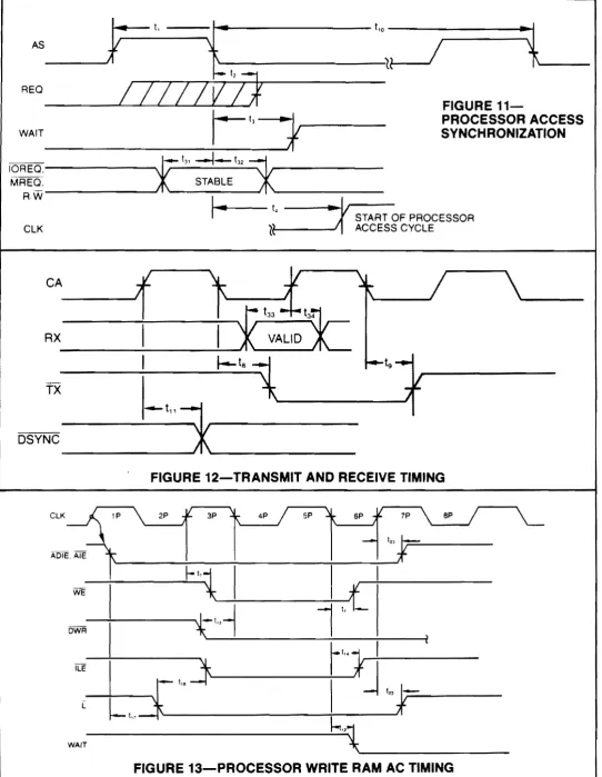
7.3 Wait Stat. G.n.rator
The COM 9026 e££ect • •
rbitrat1on .nd .ynchronou • •
cce •• to the data
p.cket buzzer and COM
9026 reg1.ter. through the u.e of
the
IIOCHRDY line.
Th.
CO.
9026
••••
r t
• •
1gn.l WAIT.t the . t . r t of a
proce ••
or 7.3 W.it St.te Generator cont •
7.4 Interrupts
The
ARCNET-PC
Interrupt
Circutt con.tsts oi Jumpers JPl through
JP7, ana ele.ents oi
A24 (74LS244).
The
COM 9026
1s capable oi
as.erting
signal
INTR
when
certain
statua bits becoae true.
Awrite to the COM 9026 MASK register speciiie. whtch status
b~tscan
generate
the
interrupt.
Ju.pera JPl through JP5 connect
s~9nalINTR to interrupt line. IRQ7 ana IRQS through IRQ2.
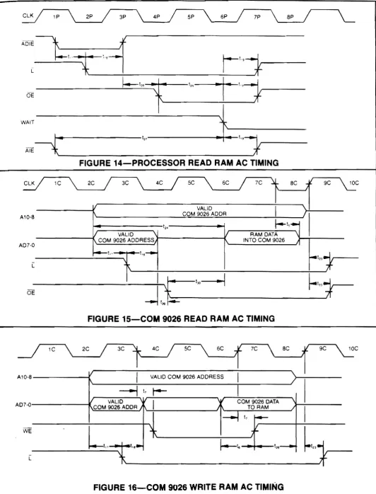
7.S Cable Tran.ceiver
The cable tran.ceiver con.ist. o£
the
CON
9032.
either
the SMC
HVC9058 or SMC HVC9068 hybira coaxial ariver, ana BNC connector J1.
The cable tran.ceiver. £unction
i . to convert TX
pulae. iroa the
COM
9026
to
a
£or.at required
by
Oatapoint ARCNET local area
network .peci£ication •• and
.1.0 to convert signal. iro.
the cable
to
NR2
aata
required
by
the
CON 9026 RX input.
The
D.tapo~ntARCNET i.ple.entation u.ea a ba.eband ay.te. with
RG62/U(93
~hM)coax.
For
a
detailed
di.cu •• ion
o£
this
imple.entation.
see
Appenaix B.O.
'.0
PROGRAftftING CONSIDERATIONS
For a de.cription o£
ba.ic
re£er
to Technical
Note
Progra •• ing the COM 9026.
COM
9026
progra •• ing considerations.
TN5-2.
AppendiX
B.O,
.ection
t1tled
When u.ing the ARCNET-PC .o£tware re.et £unction. an IO reaa
or IO
write to
10 loc.tion XX8H. where
XX value.
are deter.ined by IO
addre.. .election .witche..
will
produce
approxi.ataly
a
200
ailli.econd re.et o£ the
COM 9026
and COM 9032.
Dur1ng the t1me
--COM 9026
Local Area Network Controller
LANCTM
FEATURES
=
2.5 M bit data rate=
ARCNET"local area network controller Modified token passing protocol=
Self-reconfiguring as nodes are added or deleted from network=
Handles variable length data packets=
'6 bit CRC check and generation=
System efficiency increases with network loading=
Standard microprocessor interfaceC
Supports up to 255 nodes per networksegment
C Ability to interrupt processor at conclusion of commands
=
Interfaces to an external' K or 2K RAM buffer:J Arbitrates buffer accesses between processor
and COM 9026
c:::
Replaces over 100 MSI/SSI partsC
Ability to transmit broadcast messages==
Compatible with broadband or baseband systems=
Compatible with any interconnect media (twisted pair. coax. etc.)PIN CONFIGURATION
ET2 ( 1 '-' 40 POR
CA ( 2 39 vee
ET1 { 3 38 ~ RX
TEST2 4 37
?
rx
TESTl 5 36
P
DSYNCDWR 6 35 A8
RlW 7 34 IDOAT
IOREQ C 8 33 J 'DlD
MREQ (
9 n 3 2 A9
AS ( 10 • 31 A10
REO C 11 • 30 E'CHO
WAIT ( 12~29 ~ INTR
AlE C 13 28 ~ ADO
ADIE [ 14 27 AD1
[ ( 15 26 AD2
OE C 16 25 ADJ
WE ( 17 24 AD4
IlE C 18 23 ADS
ClK C 19 22 ADS
GND [ 20 21 AD~
Arbitrary network configurations can be used (star, tree, etc.)
Single + 5 volt supply
GENERAL DESCRIPTION
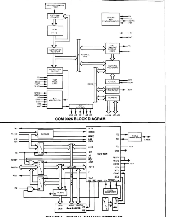
The COM 9026 is a special purpose communications adapter for interconnecting processors and intelligent peripherals using the ARCNET local area network. The ARCNET local area network is a self-polling "modified token passing" net-work operating at a 2.5 M bit data rate. A "modified token passing" scheme is one in which all token passes are acknowledged by the node accepting the token. The token passing network scheme avoids the fluctuating channel access times caused by data collisions in so-called CSMAI CO schemes such as Ethernet.
The COM 9026 circuit contains a microprogrammed se-quencer and all the logic necessary to control the token passing mechanism on the network and send and receive
data packets at the appropriate time. A maximum of 255
nodes may be connected to the network with each node being assigned a unique 10.201
The COM 9026 establishes the network configuration. and automatically re-configures the network as new nodes are added or deleted from the network. The COM 9026 per-forms address decode, CRC checking and generation, and packet acknowledgement, as well as other network man-agement functions. The COM 9026 interfaces directly to the host processor through a standard multiplexed address! data bus.
An external RAM buffer of up to 2K locations is used to hold up to four data packets with a maximum length of 508 bytes per message. The RAM buffer is accessed both by the pro-cessor and the COM 9026. The propro-cessor can write com-mands to the COM 9026 and also read COM 9026 status.
The COM 9026 will provide all signals necessary to allow
smooth arbitration of all RAM buffer operations.INT
PA1S·S
RW WR
PAD7·0
WAIT
RD
~I
~ DECODE
-Jo.,\
•
--V
,
1,
~
L:fJ.~
.... . . 1
<
•
l ' I~
"
S 4 3,
3
--ro- .1
1 G
--
•
l...
""'-- s 3 . .
~!5l!'3
1-
"-"OM
544 (' 8
8 'NTER'IAL L-_ _ _ _ _ -.J'IJ BUS
TEST MODE LOGIC
CLOCKS
AND 5VNCH!<ONIZIITION
WORKING REGlSTE!<S
_ · 5 V
_ G N D
RX
'OLD
IDDAT
INTR
Al0·118 1107·1100
COM 9026 BLOCK DIAGRAM
INTR
iOREQ
I
TX::1
CA8LE
I
MREQ
T!<ANSCEIVER
r
~ ~RlW RX CABLE
~
t..''''' ...
A1G-a
V""
~+5V...
'If--ta.
AlE CND
COM9026
AS
h
i[! TESTl
~
AOiE TEST:!
..
I"" -.a ~ ~tr~5V
IAD7·IADC AD7'() ETl
' I
;to ..
•
ET2~ I I - - I - - [
IDDAT ~
A
~ I--ii~1-- I - - ~I~~ IDLD
I-CA l51~CU<
I REO
A
t
l-8
~,.
!5l! 74LS373 (l
I
I
CLOCK
I
GENERATOR
I L I
-1"""":0"" "'Cl; '"
..
,.
~,.
~ ~ al~'T OUT
i---I
A7'()Al0-8 DI07'() ~l:!.- 1.
r-v
.a:r:..2Kx8 RAMBUFFER : e
t...!
L...-FIGURE 2-TYPICAL COM
9026 INTERFACE
I
[image:14.610.29.574.25.723.2]i I I i
I
I I I :PIN NO. NAME
31. 32, 35 ADDRESS 10, 9,S
21.22,23, . ADDRESS 24,25.26,
i
DATA 7-027,2S
I
S ! 110 REQUEST
9 MEMORY
REQUEST
7 READ/WRITE
i
10 I ADDRESS STROBE
11 REQUEST
12 WAIT
6 DELAYED
[WAITE
29 . INTERRUPT
I
REQUEST1S ilNTERFACE
LATCH ENABLE
14 ! ADDRESS!
I DATA INPUT ENABLE
13 ADDRESS
INPUT • ENABLE 15 I LATCH
i
17 WRITE
ENABLE 16
I
OUTPUT ENABLE33 '10 LOAD
34 10 DATA IN
1,3 EXTENDED
TIMEOUT FUNCTION 2, 1
37
TRANSMITDATA
38 RECEIVE
DATA
DESCRIPTION OF PIN FUNCTIONS (refer to figure 2)
I I I I I
:
I
I
i ISYMBOL FUNCTION
A 10, A9, AS These three output signals are the three most significant bits of the RAM buffer
I
address, These signals are in their high impedance state except during COM 9026 access cycles to the RAM buffer. A10 and A9 will take on the value nn as specified in the ENABLE RECEIVE or ENABLE TRANSMIT commands to orAD7-ADO lOREQ MREQ R/W AS REQ WAIT DWR INTR ILE ADIE AlE L WE OE IDLD IDDAT ET2. ET1 TX RX
from page nn and should be viewed as page select bits. For packets less than 256 by1es a 1 K buffer can be used with AS unconnected. For packets greater than 256 by1es, a 2K buffer is needed with AS connected,
These S bidirectional signals are the lower S bits of the RAM buffer address and the S bit data path in and out of the COM 9026, ADO is also used for 1/0 command
decodin of the processor contrOl or status commands to the COM 9026.
This input signal indicates that the processor is requesting the use of the data bus to receive status information or to issue a command to the COM 9026. This signal is sampled internal! on the fallin ed e of AS.
This input signal indicates that the processor is requesting the use of the data bus to transfer data to or from the RAM buffer. This signal is sampled internally on the fallin ed e of AS.
A high level on this input signal indicates that the processor's access cycle to the COM 9026 or the RAM buffer will be a read cycle. A low level indicates that a write cycle will be performed to either the RAM buffer or the COM 9026. The write
i cycle will not be completed, however, until the DWR input is asserted. This signal i
is an internal transparent latch gated with AS.
I This input si~n..l! is used by the COM 9026 to sample the state of the 10REQ, MREQ and IW inputs. The COM 9026 bus arbitration is initiated on the falling
edge of this signal. I
I
This output signal acknowledges the fact that th~ess~ or memory cycle has been sampled. The signal is equal to M EQ or 10REQ passed through : an internal transparent latch gated with AS.This output signal is asserted by the COM 9026 at the start of a processor access cycle to indicate that it is not ready to transfer data. WAIT returns to its inactive state when the COM 9026 is ready for the processor to complete its cycle.
This input signal informs the COM 9026 that valid data is present on the proces·
I
sor's data bus for write~s. The COM 9026 will remain in the WAIT state until this signal is asserted. DWR has no effect on read cycles. If the processor is able • to satisfy the write data setup time, it is recommended that this signal begrounded.
This output signal is asserted when an enabled interrupt condition has occured. INTR returns to its inactive state by resetting the interrupting status condition or the corresponding interrupt mask bit.
This output s~nal, in conjunction with
ArnE,
gates the processor's address/data bus (PAD7·P DO) onto the interface address/data bus (lAD7·IADO) during the data valid portion of a Processor Write RAM or Processor Write COM 9026 operation.This output sig!19l..enables the processor's address/data bus (PAD7·PADO) cap· tured by AS or ILE onto the interface address/data bus (IAD7·IADO).
the interface address bus (IA 10·IAS).
I
This output signal enables the processor's upper 3 address bits (PA 10·PAS) ontoThis output signal latches the interface address/data bus (IAD7·IADO) into a latch
I which feeds the lower S address bits of the RAM buffer during address valid time of all RAM buffer access cycles.
i This output signal is used as a write pulse to the external RAM buffer. Data is ref· erenced to the trailing edge of WE.
This output signal enables the RAM buffer output data onto the interface address/data bus (IAD7·IADO) during the data valid portion of all RAM buffer read operations.
This output siQnal synchronously lo~ds the v~l~e select~ by the 10 switches into an external shift register In preparation for shifting the 10 Into the COM 9026. The shift register is clocked with the same signal that feeds the COM 9026 on pin 19 (CLK). The timing associated with this signal and IDDAT (pin 34) is illustrated in fj ure19.
This input signal is the serialized output from the extemallD shift register. The 10 is shifted in most si nificant bit first. A hi h level is defined as a I ic "1".
I
I
The levels on these two input pins specify the timeout durations used by the COM !
9026 in its network protocol. Refer to the section entitled "Extended Timeout Function" for details.
This output signal contains the serial transmit data to the CABLE TRANSCEIVER.
This input signal contains the serial receive data from the CABLE TRANSCEIVER.
DESCRIPTION OF PIN FUNCTIONS (Continued)
PIN NO. NAME I SYMBOL FUNCTION
4,5
I
TEST PIN 2 . TEST PIN 1,
I
TEST2 TEST1
These input pins are grounded for normal chip operation. These pins are used in · conjunction with ET2 and ET1 to enable various internal diagnostic functions
i when performing chip level testing.
30 i ECHO
i DIAGNOSTIC
I ENABLE
I
IECHO When this input signal is low, the COM 9026 will re-transmit all messages of length less than 254 bytes. This input should be tied high for normal chip opera-, tion and is only utilized when performing chip level testing.
CLK
19
I
CLOCK ! A continuous 5 MHz clock Input used for timing 01 the COM 9026 bus cycles, bus !I ! I arbitration, seriallD input, and the internal timers.
I
i 2 CA
I
CA
I
This input signal is a 5 MHz clock used to control the operation 01 the COM 9026I
i · ~ded sequencer. This input is periodically halted in the high state by the
DSYNC output. i
I
36I
DELAYED SYNCI
DSYNC This output signal is asserted by the COM 9026 to cause the external clock gen-erator logic to halt the CA clock. Refer to figure 9.I
40
I
POWER ON POR · This input signal clears the COM 9026 microcoded sequencer pr~am counter RESETI
to zero and initializes various internal control flags and status bits. he PORsta-I
• tion of this signal will degrade the performance of the network. tus bit is also set which causes the INTR output to be asserted. Repeatedasser-I 39 1.,..5 VOLT
I
Vee Power Supplyi SUPPLY
I 20 !GROUND GND Ground
PROTOCOL DESCRIPTION
LINE PROTOCOL DESCRIPTION
The line protocol can be described as isochronous because each byte is preceded by a start interval and ended with a stop interval. Unlike asynchronous protocols, there is a con-stant amour,t of time separating each data byte. Each byte will take up exactly 11 clock intervals with a single clock inter-val being 400 nanoseconds in duration. As a result, 1 byte is transmitted every 4.4 microseconds and the time to transmit a message can be exactly determined. The line idles in a spacing (logic 0) condition. A logic '0' is defined as no line activity
and a logic 1 is defined as a pulse of 200 nanoseconds dura-tion. A transmission starts with an ALERT BURST consisting of 6 unit intervals of mark (logic 1). Eight bit data characters are then sent with each character preceded by 2 unit intervals of mark and one unit interval of space. Five types of transmis-sion can be sent as described below:
Invitations To Transmit
An ALERT BURST followed by three characters; an EOT (end ot transmission-ASCII code 04 HEX) and two (repeated) DID (Destination IDentification) characters. This message is used to pass the token from one node to another.
Free Buffer Enquiries
An ALERT BURST followed by three characters; an ENQ (ENQuiry-ASCII code 05 HEX) and two (repeated) DID (Destination IDentification) characters. This message is used to ask another node if it is able to accept a packet of data.
Data Packets
An ALERT BURST followed by the following characters: - an SOH (start of header-ASCII code 01 HEX) -a SID (Source IDentification) character
-two (repeated) DID (destination IDentification) characters.
-a single COUNT character which is the 2's comple-ment of the number of data bytes to follow if a "short packet" is being sent or 00 HEX followed by a COUNT character which is the 2's complement of the number
of data bytes to follow if a "long packet" is being sent. -N data bytes where COUNT
=
256-N (512-N for a "longpacket")
-two CRC (Cyclic Redundancy Check) characters. The CRC polynomial used is X,5 + X's + X2 + 1.
Acknowledgements
An ALERT BURST followed by one character: an ACK (ACKnowledgement-ASCII code 06 HEX) character. This message is used to acknowledge reception of a packet or as an affirmative response to FREE BUFFER ENQUIRIES.
Negative Acknowledgements
An ALERT BURST followed by one character; a NAK (Neg-ative AcKnowledgement-ASCII code 15 HEX). This mes-sage is used as a negative response to FREE BUFFER ENQUIRIES.
NETWORK PROTOCOL DESCRIPTION
if the packet is received successfully. the receiving node transmits an acknowledge message (or nothing if it is received unsuccessfully) allowing the transmitter to set the appropriate status bits to indicating successful or unsu-cessful delivery of the packet. An interrupt mask permits the COM 9026 to generate an interrupt to the processor when selected status bits become true. Figure 3 is a flow chart Illustrating the internal operation of the COM 9026.
NETWORK RECONFIGURATION
A significant advantage of the COM 9026 is its ability to adapt to changes on the network. Whenever a new node is actio vated or deactivated a NETWORK RECONFIGURArlON is performed. When a new COM 9026 is turned on (creating a new active node on the network). or if the COM 9026 has not received an INVITATION TO TRANSMIT for 840 milli· seconds, it causes a NETWORK RECONFIGURATION by sending a RECONFIGURE BURST consisting of eight marks and one space repeated 765 times. The purpose of this burst is to terminate all activity on the network. Since this burst is longer than any other type of transmission, the burst will interfere with the next INVITATION TO TRANSMIT, destroy the token and keep any other node from assuming control of the line. It also provides line activity which allows the COM
9026 sending the INVITATION TO TRANSMIT to release
control of the line.
When any COM 9026 sees an idle line for greater than 78.2 microseconds, which will only occur when the token is lost, each COM 9026 starts an internal time out equal to 146 microseconds times the quantity 255 minus its own 10. It also sets the internally stored NIO (next 10 representing the next possible 10 node) equal to its own 10. If the timeout expires with no line activity, the COM 9026 starts sending INVITATIONS TO TRANSMIT with the DID equal to the currently stored NIO. Within a given network, only one COM
9026 will timeout (the one with the highest 10 number). After
sending the INVITATION TO TRANSMIT, the COM 9026 waits for activity on the line. If there is no activity for 74.7
microseconds, the COM 9026 increments the NIO value and transmits another INVITATION TO TRANSMIT using the new NIO equal to the DID. If activity appears before the 74.7 microsecond timeout expires, the COM 9026 releases can· trol of the line. During NETWORK RECONFIGURATION. INVITATIONS TO TRANSMIT will be sent to all 256 POSSI-ble 10's. Each COM 9026 on the network will finally have saved a NIO value equal to the 10 of the COM 9026 that assumed control from it. From then until the next NET-WORK RECONFIGURATION, control is passed directly from one node to the next with no wasted INVITATIONS TO TRANSM IT sent to 10's not on the network. When a node is powered off, the previous node will attempt to pass It the token by issuing an INVITATION TO TRANSMIT. Since this node will not respond, the previous node will time out and transmit another INVITATION TO TRANSMIT to an incre-mented 10 and eventually a response will be received.
The time required to do a NETWORK RECONFIGURA-TION depends on the number of nodes in the network, the propagation delay between nodes and the highest 10 number on network but will be in the range of 24 to 61 milliseconds.
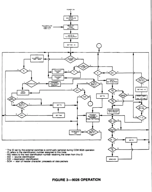
BROADCAST MESSAGES
Broadcasting gives a particular node the ability to transmit a data packet to all nodes on the network simultaneously. 10 zero is reserved for this feature and no node on the net-work can be assigned 10 zero. To broadcast a message, the transmitting node's processor simply loads the RAM buffer with the data packet and sets the destination 10 (DID) equal to zero. Figure 8 illustrates the position of each byte in the packet with the DID residing at address 01 HEX of the current page selected in the TRANSMIT command. Each individual node has the ability to ignore broadcast mes-sages by setting the most signficant bit of the ENABLE RECEIVE TO PAGE nn command (see "WRITE COM 9026 COMMANDS") to a logic zero.
COM 9026 OPERATION BUFFER CONFIGURATION
During a transmit sequence, the COM 9026 fetches data from the Transmit Buffer, a 256 (or 512) byte segment of the RAM buffer. The appropriate buffer size is specified in the DEFINE CONFIGURATION command. When long pack-ets are enabled, the COM 9026 will interpret the packet as a long or short packet depending on whether the contents
FIGURE
8-RAM BUFFER
PACKET
CONFIGURATION
ADDRESS o 1 2 FORMAT SID DID COUNT; 256 - NNOT _ _ U,=-,S"",E~D _ _ _
COUNT DATA BYTE 1
255 511 _--=-DA=TA~B'f:r~~
•
•
•
DATA BYTE N-1 DATABYTEN
NOT
SHORT PACKET (256 OR 512 BYTE PAGE)
205
of buffer location 02 is zero or non zero. During a receive sequence, the COM 9026 stores data in the receive buffer, also a 256 (or 512) byte segment of the RAM buffer. The processor 1/0 command which enables either the COM 9026
receiver or the COM 9026 transmitter also initializes the respective buffer page register. The formats of the buffers (both 256 and 512 byte) are shown below.
ADDRESS 0 2 3 COUNT 511 DID 0
COUNT;512 N NOT USED
•
•
•
LONG PACKET (512 BYTE PAGE)N = DATA PACKET LENGTH SID = SOURCE 10 DiD = DESTINATION 10
[image:17.610.44.571.572.742.2]PO~I:iON
N
• The 10 set by the external switches is continually sampled during COM 9026 operation • 10 refers to the identification number assigned to this node
- NID refers to the next identification number receiving the token from this 10 - SID = source identification
• DID
=
destination identification [image:18.610.32.563.50.718.2]- SOH start of header character; preceeds all data packets
PROCESSOR INTERFACE
Figure 2 illustrates a typical COM 9026 to processor inter-face. The signals on the left side of this figure represent typ-ical processor signals with a 16 bit address bus and an B bit 1ata bus with the data bus multiplexed onto the lower B address lines (PAD7-PADO). The processor sees a net-work node (a node consists of a COM 9026, RAM buffer, cable transceiver. etc. as shown in figure 2) as 2K memory locations and 4 I 0 locations within the COM 9026. The RAM buffer is used to hold data packets temporarily prior to transmission on the network and as temporary stor-age of all received data packets directed to the particular node. The Size of the buffer can be as large as 2K by1e loca-tions providing four pages at a maximum of 512 by1es per page. For packet lengths smaller than 256 by1es, a , K RAM buffer can be used to provide four pages of storage. In this case address line lAB (sourced from either the COM 9026 or the processor) should be left unconnected. Since four pages of RAM buffer are provided, both transmit and receive operations can be double buffered with respect to the pro-cessor. For instance, after one data packet has been loaded into a particular page within the RAM buffer and a transmit command tor that page has been issued, the processor can start loading another page with the next message in a multi-message transmission sequence. Similarly, after one mes-sage is received and completely loaded into one page of the RAM buffer by the COM 9026, another receive com-mand can be issued to allow reception of the next packet while the first packet is read by the processor. In general, the four pages in the RAM buffer can be used for transmit or receive in any combination. In addition. the processor
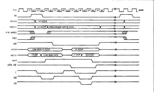
CLK~~~6P
will also use the interface bus (IA' O-IAB, IAD7-IADO) when performing 1/0 access cycles (status reads from the COM
9026 or command writes to the COM 9026).
To accomplish this double buffering scheme. the RAM buffer must behave as a dual port memory. To allow this RAM to be a standard component. arbitration and control on the interface bus (IA10-IAB. IAD7-IADO) is required to permit both the COM 9026 and the processor access to the RAM buffer and. at the same time, permit all processor 110 oper-ations to or from the COM 9026.
Processor access cycle requests begin on the trailing edge of AS if either 10REO or MREO is asserted. These access cycles run completely asynchronous with respect to the COM 9026. Because of this, upon processor access cycle requests. the COM 9026 immediately puts the processor into a wait state by asserting the WAIT output. This gives the COM 9026 the ability to synchronize and control the processor access cycle. When the processor access cycle is synchronized by the COM 9026, the WAIT Signal is even-tually removed allowing the processor to complete its cycle. For processor RAM buffer access cycles, AlE and ADIE enable the processor address captured during AS time onto the l.nterface address bus (IA 10-IAB, IAD7-IADO). The sig-nal L will capture the B least significant bits of this address (appearing on IAD7-IADO) before the data is multiplexed onto it. At the falling edge of L, a stable address is pre-sented to the RAM buffer. For read cycles. OE allows the addressed RAM buffer data to source the interface addreSS! data bus (IAD7-IADO). In figure 2, this information is passed into a transparent latch gated with WAIT. At the falling edge of WAIT, the data accessed by the processor is captured
~ooo
AS~~r _ _ _ _ _ _ _ _ _ _ _ _ _ _ _ _ _ _ _ _ _ _ _ _ _ _ _ _ _ _ _ _ -4I~
PA 158 )( HI AOOR
U
::===x----PA07·Q _ _ _ ...i
X
LO AOORq~f--
___
---IX
RAM Doc, X'---4;O----MREO _ _\~\w\\~
_ _
...JruG~~ll~---~:~:~ZuZ~/Z
REO 1~7T.77r---tn~---~ll
\\\\
RO _ _ _ _ _ _ _ _ _ _
~~~l---~\---~l~l---iA10·8 ---itr-<::::::t!HI~A;QOQ!ORL==»---«:::::JC~O~M:290~2~6 ~HI~AQ!OO~Rc:==)>---;t~l ---~- IA07·0 ---4t~ RAM OCL'>--<~J~~'1!'~:8~g~=»--""'(C~:·M~C=)>---HU---r
lWAIT _ _ _ _ _ _ ...J
\
~---4H~---
---4n~---I~
[ - - - 1
l~I
\
I
~--4n~---H
~---~
\
I
\
I
11
AlE
- - - 1
H,
[image:19.610.31.574.383.698.2]r---tl~l---I
FIGURE 4-PROCESSOR READ RAM FOLLOWED BY COM 9026 READ RAM
and driven out via the logic function RD anded with REO. For processor 110 read cycles from the COM 9026, ADIE and AlE are used to enable the processor address into the COM 9026. Data out of the COM 9026 is gated through the transparent latch and appears on the processor's data bus with the same control signals used for RAM read cycles.
For processor write cycles. after the falling edge of
C.
the COM 9026 produces a WE (write enable) output to the RAM buffer. and the ILE output from the COM 9026 allows the processor data to source the interface address/data bus (IAD7-IADO). At this time the COM 9026 waits for DWR before concluding the cycle by removing the WAIT output. DWR should only be used if the processor cannot deliver the data to be written in enough time to satisfy the write setup time requirements of the RAM buffer. By delaying the acti-vation of DWR. the period of the write cycle will be extended until the write data is valid. Since the architecture and oper-ation of the COM 9026 requires periodic reading and writ-ing of the RAM buffer in a timely manner, holdwrit-ing the DWR input off for a long period of time, or likewise by running the processor at a slow speed, can result in a data overflow condition. It is therefore recommended that if the processor write data setup time to the RAM buffer is met, then the DWR input should be grounded.For processor 110 write cycles to the COM 9026. ADIE and AlE are used to enable the processor's address onto the interface data bus. ILE is used to enable the processor's write data into the COM 9026. Delaying the activation of DWR will hold up the COM 9026 cycle requiring the same precautions as stated for Processor RAM Write cycles.
elK
As stated previously, processor requests Occur at the fall. ing edge of AS if either 10REO or MREO are active. COM 9026 requests occur when the transmitter or receiver need to read or write the RAM buffer in the course of executing the command. If the COM 9026 requests a bus cycle at tne same time as the processor. or shortly after the processor. the COM 9026 cycle will follow immediately after the pro. cessor cycle. Figure 4 illustrates the timing relationship of a Processor RAM Read cycle followed by a COM 9026 RAM read cycle. Once the AS signal captures the processor address to the RAM buffer and requests a bus cycle, it takes 4 CLK periods for the processor cycle to end. Figure 4 breaks up these 4 CLK periods into 8 half clock interval labeled 1 P through 8P. A COM 9026 access cycle will take 5 CLK periods to end. Figure 4 breaks up these 5 CLK periods into 10 half intervals labeled lC through lOCo
If a processor cycle request occurs after a COM 9026 request has already been granted, the COM 9026 cycle will occur first, as shown in figure 5. Figure 5 illustrates the timing relationship of a COM 9026 RAM Write cycle followed by a Processor RAM Write cycle. Due to the asynchronous nature of the bus requests (AS and CLK), the transition from the end of the COM 9026 cycle to the beginning of the proces· sor cycle might have some dead time. Refering to figure 5. if AS falling edge occurs after the start of half CLK interval 9C, no real contention exists and it will take between 200 and 500 nanoseconds before the processor cycle can start. The start of the processor cycle is defined as the time when the COM 9026 produces a leading edge on both ADIE and AlE. If the processor request occurs before the end of half
r-u-LJLooo
As ____
~1 \~_________________________________
~ ~PA1S·8 _ _ _ _ -'X\...:H:.::.I.:;;,A:;,:DD::::..R:....-_ _ _ _ _ _ _ _ _ _ _ _ _ _ _ _
----j~"---PAD7·Q _ _ _ _
-'1
lO ADDRX
PROCESSOR WRITE DATAX'l.... __
--.:u:._--...jX'-___ _
Rw.MREo _ _ _ ~\~~~\~ _ _ ~'~II~
__________________
~~!~~ _ _ ~I~/uOREO
1111
II\\\
,
WR
\'I.... ______________
~ IIU
( HI ADDR )
IA10-8 ----«C3]CO~M~90~26[!H!!:1 A~D~D~R===»--_C~~[:===:>----t ...
-IAD7-0 (
mOOR
X
COM 9026 DATA ) ( ,,:< '00"X
":W$~ ) UWAIT ,
\
II
ADIE. AlE - - - , .
\
I
Uc
\\.. _ _ _ _ _ _ ...JI
\
I
U\'---,
\
I
II [image:20.610.34.557.374.686.2]ILE
\
I
u
FIGURE 5-COM 9026 WRITE RAM FOLLOWED BY PROCESSOR WRITE RAM
r
f
ClK interval 5C (figure 5 illustrates this situation), then the processor cycle will always start at half ClK interval 1
P.
The uncertainty is introduced when the processor request occurs during half ClK intervals 6C, 7C or 8C. In this case, the processor cycle will start between 200 and 500 nanose-conds later depending on the particular timing relation between AS and ClK. The maximum time between pro-cessor request and propro-cessor cycle start. which occurs when the processor request comes just after a COM 9026 request.IS 1300 nanoseconds. It should be noted that all times specified above assume a nominal ClK period of 200 nanoseconds.
Figures 6 and 7 illustrate timing for Processor Read COM 9026 and Processor Write COM 9026 respectively. These cycles are also shown divided into 8 half clock intervals (1 P through 8P) and can be inserted within figures 4 and 5 if these processor cycles occur.
POWER UP AND INITIALIZATION
The COM has the following power up requirements:
1-The POR input must be active for at least 100 milliseconds.
2-The ClK input must run for at least 10 clock cycles before the POR input is removed.
3-While POR is asserted, the CA input may be running or held high. If the CA input is running, POR may be released asynchronously with respect to CA. If the CA input is held high. POR may be released before CA begins running.
During POR the status register will assume the following state:
BIT 7 (RI) set to a logiC "1 ". BIT 6 (ETS2) not affected BIT 5 (ETS 1) not affected BIT 4 (POR) set to a logic "1". BIT 3 (TEST) set to a logic "0".
CLK~
AS~ll---PA15.a-=:J. HIACDR :ll-l _ _ _ _ _ _ _ _ _ _ PAD7-0 -=:J., LO ADDR)----1~ :OM 9025 DATA OUT
~'l-l---RD _ _ _ _ - - . l
r "
H
REO IIV
IA10-8 ---llH::BH!:!1
A~DD~R==::J)_---'AD7·0 ---Il~CO ...
90260Ar.OUT)--WAIT _ _ _ _
....Jr
l ,-AOIE
!~---Ale
---l.H-\
, ,
-FIGURE 6-PROCESSOR READ COM 9026
209
BIT 2 (RECON) set to a logic "0". BIT 1 (TMA) set to a logiC
"a".
BIT 0 (TA) set to a logiC "1 ".In addition the DSYNC output is reset inactive high and the interrupt mask register is reset (no maskable interrupts enabled). Page 00 is selected for both the receive and the transmit RAM buffer. After the POR signal is removed. the COM 9026 will generate an interrupt from the nonmaskable Power On Reset interrupt. The COM 9026 will start oper-ation four CA clock cycles after the POR signal is removed. At this time. the COM 9026. after reading its ID from the external shift register. will execute two write cycles to the RAM buffer. Address 00 HEX will be written with the data D1 HEX and address 01 HEX will be written with the ID number as previously read from the external shift register. The processor may then read RAM buffer address 01 to determine the COM 9026 ID. It should be noted that the data pattern D1 written into the RAM has been chosen arbitrar-ily. Only if the D1 pattern appears in the RAM buffer can proper operation be assured.
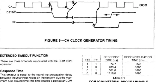
CLOCK GENERATOR
[image:21.610.33.574.275.736.2]The COM 9026 uses two separate clock inputs namely CA and ClK. The ClK input is a 5 MHz free running clock and the CA input is a start/stop clock periodically stopped and started to allow the COM 9026 to synchronize to the incom-ing data that appears on the RX input.
Figure 9 illustrates the timing of the CA clock generator and its relationship to the DSYNC output and the RX input. The DSYNC output is used to control the stopping of the CA clock. On the next rising edge of the CA input after DSYNC is asserted, CA will remain in the high state. The CA clock remains halted in the high state as long as the RX signal remains high. When the RX signal goes low. the CA clock is restarted and remains running until the next falling edge of DSYNC. (See figure 20 for an implementation of this circuit.)
CLK~
AS-1 \ l l r -PAls·a
---v
HI AOOR i l---II It
PA07.0.::::x LOW AOOR x:::::!:~~~ROC=ES::::-:SO::::R7.'W""'RI-:::;TE:-:::O""'AT"....A
--r=::..
I'.-...
HRW~_~~~_~liL_~ ______ ~ ____________ __
WR
~l~---~,---
n~----~l~l---REQ---I.i.LI
IA10-a ---~n-_{C:?:HIC!A§!OO~R==:>_)
-IA07 a _ _ _ _ _
~>-...r:-;"III!.aoc~.!f~SO"~)r---.... • \. ~~Fmt9 ... TA,
\
... [image:21.610.184.556.451.711.2]_--'---ILE ---~Hr--... \'__...JI
CA
000
Rx---~l~---FIGURE 9-CA CLOCK GENERATOR TIMING
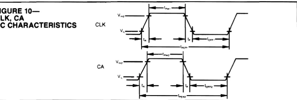
EXTENDED TIMEOUT FUNCTION
There are three timeouts associated with the COM 9026 operation.
Response Time
This timeout is equal to the round trip propagation delay between the 2 furthest nodes on the network plus the max-imum turn around time (the time it takes a particular COM 9026 to start sending a message in response to a received message) which is known to be 12 microseconds. The round trip propagation delay is a function of the transmission media and network topology. For a typical system using RG62 coax in a baseband system, a one way cable propagation delay of 31 microseconds translates to a distance of about 4 miles. The flow chart in figure 3 uses a value of 74.7 microsec-onds (31 31 ~ 12 + margin) to determine if any node will respond.
Idle Time
This time is associated with a NETWORK RECONFIGUR-ATION. Refering to figure 3, during a NETWORK RE-CONFIGURATION one node will continually transmit INVI-TATIONS TO TRANSMIT until it encounters an active node. Every other node on the network must distinguish between this operation and an entirely idle line. During NETWORK RECONFIGURATlON, activity will appear on the line every 78 microseconds. This 78 microsecond is equal to the response time of 74.7 microseconds plus the time it takes the COM 9026 to retransmit another message (usually another INVITATION TO TRANSMIT). The actual timeout is set to 78.2 microseconds to allow for margin.
Reconfiguration Time
If any node does not receive the token within this time, the node will initiate a NETWORK RECONFIGURATION. The ET2 and ET1 inputs allow the network to operate over longer distances than the 4 miles stated earlier. DC levels on these inputs control the maximum distances over which the COM 9026 can operate by controlling the 3 timeout val-ues described above. Table 1 illustrates the response time and reconfiguration time as a function of the ET2 and ET1 Inputs. The idle time will always be equal to the response time plus 3.5 microseconds. It should be noted that for proper
network operation, aI/ COM 9026's connected to the same network must have the same response time, idle time and reconfiguration time.
ET1 1
o
I 1o
RESPONSE TIME (f..l.s)
74.7 283.4 561.8 1118.6
RECONFIGURATION TIME (ms)
840 1680 1680 1680
TABLE 1
COM 9026 INTERNAL PROGRAMMABLE
TIMER VALUES
1/0 COMMANDS
10 commands are executed by activating the 10REQ input The COM 9026 will interrogate the ADO and the R W inputs at the AS time to execute commands according to the fol-lowing table:
10REQ
i
ADOi
RiW!
.
FUNCTION lowI
low . low I write Interrupt masklow I low high read status register low I high low write COM 9026 command
low I high . high I reserved for future use
READ STATUS REGISTER
Execution of this command places the contents of the sta-tus register on the data bus (AD7 -ADO) during the read por-tion of the processor's read cycle. The COM 9026 status register contents are defined as follows:
BIT 7 -Receiver inhibited (RI)-This bit. if set high. indi-cates that a packet has been deposited into the RAM buffer page nn as specified by the last ENABLE RECEIVE TO PAGE nn command. The setting of this bit can cause an interrupt via INTR if enabled during a WRITE INTERRUPT MASK command. No messages will be received untit an ENABLE RECEIVE TO PAGE nn command is issued. After any message is received, the receiver is automat-ically inhibited by setting this bit to a logic one. BIT 6-Extended Timeout Status 2 (ETS2)-This bit
re-flects the current logic value tied to the ET2 input pin (pin 1).
BIT 5-Extended Timeout Status 1 (ETS1)-This bit re-flects the current logic value tied to the ET1 input pin
(pin 3).