8 ISSN: 2278 – 7798 All Rights Reserved © 2015 IJSETR
Abstract— This project introduces and evaluates an auxiliary control strategy for downstream fault current interruption in a radial distribution line by means of a dynamic voltage restorer (DVR). The proposed controller supplements the voltage-sag compensation control of the DVR. It does not require phase-locked loop and independently controls the magnitude and phase angle of the injected voltage for each phase. Fast least error squares digital filters are used to estimate the magnitude and phase of the measured voltages and effectively reduce the impacts of noise, harmonics, and disturbances on the estimated phasor parameters, and this enables effective fault current interrupting even under arcing fault conditions.The main drawback of this approach is that the dc-link voltage of the DVR increases due to real power absorption during fault current-limiting operation and necessitates overcome the aforementioned limitations, this project proposes an augmented control strategy for the dvr that provides: 1) voltage-sag compensation under balanced and unbalanced conditions and 2) a fault current interruption (FCI) function.a switch to bypass the DVR when the protective relays, depending on the fault conditions, do not rapidly clear the fault.
The adopted DVR converter is comprised of three independent H-bridge VSCs that are connected to a common dc-link capacitor. These VSCs are series connected to the supply grid, each through a single-phase transformer. The proposed FCI control system consists of three independent and identical controller’s one for each single-phase VSC of the DVR. This paper introduces an auxiliary control mechanism to enable the DVR to interrupt downstream fault currents in a radial distribution feeder. The current ripples can be reduced by using SVPWM technique.
This control function is an addition to the voltage-sag compensation control of the DVR. The performance of the proposed controller, under different fault scenarios, including arcing fault conditions, is investigated based on time-domain simulation studies in the MATLAB/SIMULINK environment. Index Terms—Digital filters, dynamic voltage restorer (DVR), fault current interrupting, multi loop control, Space vector pulse width modulation (SVPWM).
I. INTRODUCTION
Voltage sag, voltage swell and harmonics are major power quality problems concern of the industrial and commercial electrical consumers due to enormous loss in terms of time and money. This is due to the advent of a large numbers of sophisticated electrical and electronic equipment,
such as computers, programmable logic controllers, variable speed drives, and so forth. The use of this equipment often requires very high quality power supplies.
Some special equipment are sensitive to voltage disturbances, especially if these take up to several periods, the circuit does not work. Therefore, these adverse effects of voltage changes necessitate the existence of effective mitigating devices. There are various solutions to these problems. One of the most effective solutions is the installation of a Dynamic Voltage Restorer (DVR). DVR is a series custom power device, which has excellent dynamic capabilities. It is well suited to protect sensitive loads from duration voltage sag or swell. A DVR is basically a controlled voltage source installed between the supply and a sensitive load. It injects a voltage on the system in order to compensate any disturbance affecting the load voltage. Basic operating principle of a DVR is as shown in Fig.1.
In August 1996, Westinghouse Electric Corporation installed world’s first dynamic voltage restorer in Duke Power Company’s 12.47 kV substation in Anderson, South Carolina. This was installed to provide protection to an automated rug manufacturing plant. Prior to this connection, the restorer was first installed at the Waltz Mill test facility near Pittsburgh for full power tests.THE dynamic voltage restorer (DVR) is a custom power device utilized to counteract voltage sags [2], [3]. It injects controlled three-phase ac voltages in series with the supply voltage, subsequent to a voltage sag, to enhance voltage quality by adjusting the voltage magnitude, wave shape, and phase angle [4]–[7]. The main components of a DVR (i.e., a series transformer𝑇𝑆, a voltage - source converter (VSC), a harmonic filter, a dc-side capacitor𝐶𝐷𝐶, and an energy storage device [8], [9]). The line-side harmonic filter [6] consists of the leakage inductance of the series transformer 𝐿𝑓and the filter capacitor𝐶𝑓.
A Versatile Control Scheme for the Fault current
Interruption by using Dynamic Voltage Restorer
JANARDHAN DAMA, M. Tech scholar & D. REVATHI, M. Tech, Head of the Department
Electrical and Electronics Engineering, KIET College, Kakinada
9 ISSN: 2278 – 7798 All Rights Reserved © 2015 IJSETR
Fig. 1 Schematic diagram of a DVR with a line-side harmonic filter.
The DVR is conventionally bypassed during a downstream fault to prevent potential adverse impacts on the fault and to protect the DVR components against the fault current [10]–[12]. A technically elaborate approach to more efficient utilization of the DVR is to equip it with additional controls and enable it also to limit or interrupt the downstream fault currents. A control approach to enable a DVR to serve as a fault current limiter is provided in [10]. The main drawback
.
Fig 2. Per-phase block diagram of the DVR control system in FCI mode.
of this approach is that the dc-link voltage of the DVR increases due to real power absorption during fault current-limiting operation and necessitates a switch to bypass the DVR when the protective relays, depending on the fault conditions, do not rapidly clear the fault. The dc-link voltage increase can be mitigated at the cost of a slow-decaying dc fault current component using the methods introduced in [8] and [13].
To overcome the aforementioned limitations, this paper proposes an augmented control strategy for the dvr that provides: 1) voltage-sag compensation under balanced and unbalanced conditions and 2) a fault current interruption (fci) function. The former function has been presented in [14] and the latter is described in this paper.
It should be noted that limiting the fault current by the DVR disables the main and the backup protection (e.g., the distance and the over current relays). This can result in prolonging the fault duration. Thus, the DVR is preferred to reduce the fault current to zero and interrupt it and send a trip signal to the upstream relay or the circuit breaker (CB).
It should be noted that the FCI function requires 100% voltage injection capability. Thus, the power ratings of the series transformer and the VSC would be about three times those of a conventional DVR with about 30%–40% voltage injection capability. This leads to a more expensive DVR system. Economic feasibility of such a DVR system depends on the importance of the sensitive load protected by the DVR and the cost of the DVR itself.The performance of the
proposed control scheme is evaluated through various simulation studies in the MATLAB/SIMULINK platform. The study results indicate that the proposed control strategy: 1) limits the fault current to less than the nominal load current and restores the PCC voltage within less than 10 ms, and interrupts the fault current within two cycles; 2) it can be used in four- and three-wired distribution systems, and single-phase configurations; 3) does not require phase-locked loops; 4) is not sensitive to noise, harmonics, and disturbances and provides effective fault current interruption even under arcing fault conditions; and 5) can interrupt the downstream fault
current under low dc-link voltage conditions.
II. PROPOSEDFCICONTROLSTRATEGY The adopted DVR converter is comprised of three independent H-bridge VSCs that are connected to a common dc-link capacitor. These VSCs are series connected to the supply grid, each through a single-phase transformer. The proposed FCI control system consists of three independent and identical controller’s one for each single-phase VSC of the DVR.
Assume the fundamental frequency components of the supply voltage, load voltage, and the injected voltage, Fig. 1 are
(1)
(2)
(3) Two identical least error squares (LES) filters [14] are used to estimate the magnitudes and phase angles of the phasors corresponding 𝑉𝑆to𝑉𝑖𝑛𝑗(𝑖. 𝑒. . , 𝑉 =𝑉𝑆 𝑆∠𝜃𝑆 and (i.e., and V =inj Vinj∠θinj .
The FCI function requires a phasor parameter estimator (digital filter) which attenuates the harmonic contents of the measured signal. To attenuate all harmonics, the filter must have a full-cycle data window length which leads to one cycle delay in the DVR response. Thus, a compromise between the voltage injection speed and
10 ISSN: 2278 – 7798 All Rights Reserved © 2015 IJSETR
disturbance attenuation is made. The designed LES filters utilize a data window length of 50 samples at the sampling rate of 10 kHz and, hence, estimate the voltage phasor parameters in 5 ms. Fig. 3 depicts the frequency response of the LES filters and indicates significant attenuation of voltage noise, harmonics, and distortions at frequencies higher than 200 Hz and lower than 50 Hz. Reference [13] demonstrates the effectiveness of this filter in attenuating the noise, harmonics, and distortions for the sag compensation mode of operation as well. The next section shows that this filter also performs satisfactorily in the FCI operation mode, even under arcing fault conditions where the measured voltage and current signals are highly distorted.
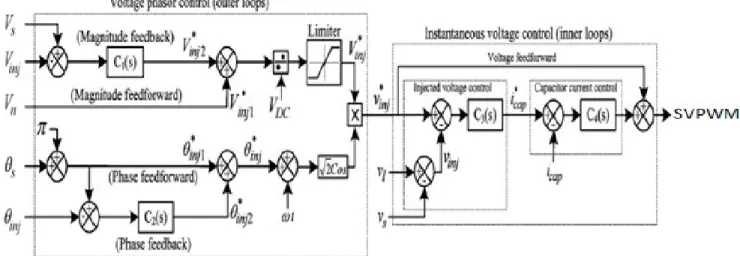
Fig. 2 shows a per-phase block diagram of the proposed DVR control system corresponding to the FCI operation mode, where is the nominal rms phase voltage. The control system of Fig. 2 utilizes 𝑣𝑠,𝑣𝑙 , the dc-link voltage𝑉𝐷𝐶 , and the harmonic filter capacitor current 𝑖𝑐𝑎𝑝,as the input signals. The reported studies in this paper are based on the over current fault detection method of [7] and [12]. The fault detection mechanism for each phase is activated when the absolute value of the instantaneous current exceeds twice the rated load current.
The proposed multi loop control system [3], [8], [9], [15]–[20] includes an outer control loop (voltage phasor control) and an inner control loop (instantaneous voltage control). The inner loop provides damping for the transients caused by the DVR harmonic filter [18] and [21], and improves the dynamic response and stability of the DVR. The inner loop is shared by the sag compensation and the FCI functions. When a downstream fault is detected, the outer loop controls the injected voltage magnitude and phase angle of the faulty phase(s) and reduces the load-side voltage to zero, to interrupt the fault current and restore the PCC voltage. The DVR ―outer‖ voltage phasor control and ―inner‖ instantaneous voltage control, corresponding to each phase, are described in the following two subsections.
A. Voltage Phasor Control System
In the FCI operation mode, the required injected voltage phasor is equal to the source voltage phasor, but in phase opposition [i.e., the injected phasor V = Vinj inj∠θinj is controlled to be𝑉𝑆∠(𝜃𝑆+ 𝜋)]. Performance of the voltage phasor control, in terms of transient response, speed, and
steady-state error, is enhanced by independent control of voltage magnitude and phase, and incorporating feed forward signals to the feedback control system [17], [18], [21]–[27]. Fig. 2 shows two proportional- integral (PI) controllers ( and ) that are used to eliminate the steady-state errors of the magnitude and phase of the injected voltage, respectively. Parameters of each controller are determined to achieve a fast response with zero steady-state error.
The output of the phasor control system is a reference phasor denoted by𝑉 = 𝑉𝑖𝑛𝑗∗ 𝑖𝑛𝑗∗ ∠𝜃𝑖𝑛𝑗∗ . To eliminate the effects of the dc-link voltage variations on the injected voltages, 𝑉𝑖𝑛𝑗 ∗ is normalized by 𝑉𝑑𝑐 . The magnitude and the phase angle of 𝑉 𝑖𝑛𝑗∗ are independently calculated and the magnitude is passed through a limiter (Fig. 2). The resulting phasor magnitude and phase angle are converted to the sinusoidal signal 𝑉𝑖𝑛𝑗∗ , which is the reference signal for the instantaneous voltage control. B. Instantaneous Voltage-Control System
Under ideal conditions, a voltage sag can be effectively compensated if the output of the phasor-based controller𝑉𝑖𝑛𝑗∗ , is directly fed to the sinusoidal pulse-width modulation (SPWM) unit. However, resonances of the harmonic filter cannot be eliminated under such conditions. Therefore, to improve the stability and dynamic response of the DVR, an instantaneous injected voltage controller and a harmonic filter capacitor current controller are used to attenuate resonances.
The generated reference signal for the injected voltage 𝑉𝑖𝑛𝑗∗ is compared with the measured injected voltage 𝑉𝑖𝑛𝑗, and the error is fed to the voltage controller. As shown in Fig. 2, the output of the voltage controller 𝑖𝑐𝑎𝑝 ,∗ is the reference signal for the filter capacitor current control loop. It is compared with the measured capacitor current 𝑖𝑐𝑎𝑝, and the error is fed to the current controller.
The steady-state error of the proposed control system is fully eliminated by the PI controllers in the outer control loop (i.e., 𝐶1 and 𝐶2 ), which track dc signals (magnitude and phase angle). Therefore, there is no need for higher order controllers in the inner control loop which are designed based on sinusoidal references. Thus, in Fig. 2, 𝐶3and 𝐶4are pure gains𝑘𝑣 and 𝐾𝑐, respectively.
A large 𝑘𝑣 result in amplification of the DVR filter resonance and can adversely impact the system stability [18]. Thus, the transient response of the DVR is enhanced by a feed forward loop, and a small proportional gain is utilized as the voltage controller.
A large 𝐾𝑐 damps the harmonic filter resonance more effectively, but it is limited by practical considerations (e.g., amplification of capacitor current noise, measurement noise, and dc offset [18]). Therefore, the lowest value of the proportional gain which can effectively damp the resonances is utilized. The output of the current controller is added to the feed forward voltage to derive the signal for the PWM generator.
11 ISSN: 2278 – 7798 All Rights Reserved © 2015 IJSETR
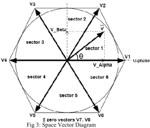
III. SPACE VECTOR PWM
The Space Vector PWM generation module accepts modulation index commands and generates the appropriate gate drive waveforms for each PWM cycle. This section describes the operation and configuration of the SVPWM module.
A inverter with dc link configuration can have eight possible switching states, which generates output voltage of the inverter. Each inverter switching state generates a voltage Space Vector (V1 to V6 active vectors, V7 and V8 zero voltage vectors) in the Space Vector plane (Figure: space vector diagram). The magnitude of each active vector (V1to V6) is 2/3 Vdc (dc bus voltage).
The Space Vector PWM (SVPWM) module inputs modulation index commands (V_Alpha and V_Beta) which are orthogonal signals (Alpha and Beta) as shown in Figure. The gain characteristic of the SVPWM module is given in Figure3 . The vertical axis of Figure represents the normalized peak motor phase voltage (V/Vdc) and the horizontal axis represents the normalized modulation index (M).
Fig 3: Space Vector Diagram
Over modulation occurs when modulation Umag > Umag L. This corresponds to the condition where the voltage vector in (Figure: voltage vector rescaling)increases beyond the hexagon boundary. Under such circumstance, the Space Vector PWM algorithm will rescale the magnitude of the voltage vector to fit within the Hexagon limit. The magnitude of the voltage vector is restricted within the Hexagon; however, the phase angle (θ) is always preserved. The transfer gain (Figure: transfer characteristics) of the PWM modulator reduces and becomes non-linear in the over modulation region.
Fig3a: Transfer Characteristics IV SIMULATION RESULTS
Fig. 4 depicts a single-line diagram of a power system which is used to evaluate the performance of the proposed DVR control system under different fault scenarios, in the MATLAB/SIMULINK software environment. A 525-kVA DVR system is installed on the 0.4-kV feeder, to protect a 500-kVA, 0.90 lagging power factor load against voltage sags. Parameters of the simulated power system and the DVR are given in Appendix A. In the reported studies, the base voltage for per-unit values is the nominal phase voltage. Besides, voltage and current waveforms of phases A, B, and C are plotted by solid, dashes, and dotted lines, respectively.
Fig. 4. Single-line diagram of the system used for simulation studies.
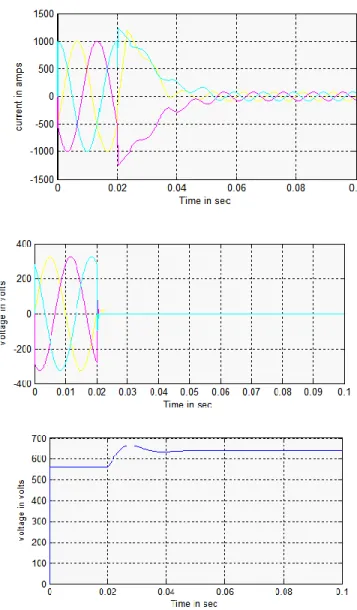
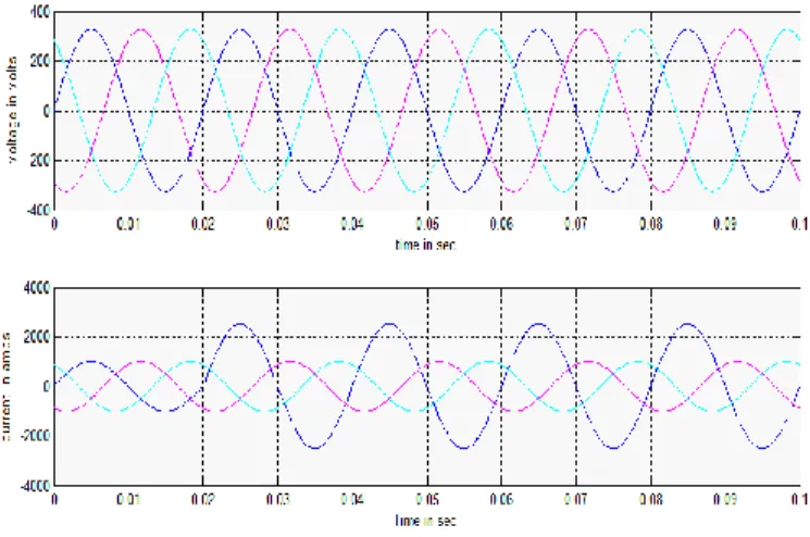
Fig. 5. (a) Voltages at bus3. (b) Fault currents, during downstream three-phase fault when the DVR is inactive (bypassed).
12 ISSN: 2278 – 7798 All Rights Reserved © 2015 IJSETR
The system is subjected to a three-phase short circuit with a negligible fault resistance at t=20 ms at𝐵𝑈𝑆 5 . Prior to the fault inception, the DVR is inactive (in standby mode) (i.e., the primary windings of the series transformers are shorted by the DVR). During the fault if the DVR is bypassed, the voltage at Bus3 drops to 0.77 p.u. and the fault current increases to about 17 times the rated load current (Fig. 5). Fig. 6 shows FCI performance of the proposed DVR control system during the fault. Fig. 6(a)–(c), respectively, shows the phase injected voltages, the restored three-phase supply-side voltages, and the three-three-phase load-side voltages which are reduced to zero to interrupt the fault currents. The slightly injected voltage by the DVR before the fault initiation [Fig. 6(a)] is the voltage drop across the series impedance of the DVR series transformer secondary winding.
Fig. 6(d) shows the line currents (i.e., the currents passing through the DVR). Fig. 6(d) illustrates that the proposed FCI method limits the maximum fault current to about 2.5 times the nominal value of the load current and interrupts the fault currents in less than 2 cycles. Fig. 6(e) depicts variations of the dc-link voltage during the FCI operation, and indicates that the dc-link voltage rise under the worst case (i.e., a severe three phase fault) is about 15% and occurs during the first 5 ms after fault inception.
Fig6. (a) Injected voltages. (b) Source voltages. (c) Load voltages. (d) Line currents. (e) DC-link voltage, during the
13 ISSN: 2278 – 7798 All Rights Reserved © 2015 IJSETR
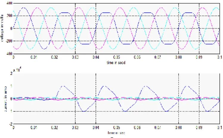
Fig. 7. (a) Voltages at BUS 3 , (b) Fault currents, during
downstream phase-to phase fault when the DVR is inactive (bypassed).
B. Phase-to-Phase Downstream Faults
The system of Fig. 4 is subjected to a phase-A to phase-C fault with the resistance of 0.05 Ω at 10% of the cable length connecting BUS 4to BUS 5, at 20 ms. When the DVR is
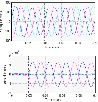
inactive (bypassed) during the fault (Fig. 7), the PCC voltage drops to 0.88 p.u., and the fault current increases to about 11 times the rated load current. Fig. 8 illustrates that when the DVR is in service, the proposed FCI control successfully interrupts the fault current and restores the PCC voltage of the faulty phases within two cycles. Fig. 8(e) shows that the dc-link voltage rise is less than 7%. Fig. 8 also shows that only the two faulty phases of the DVR react, and the healthy phase is not interrupted.
Fig. 8. (a) Injected voltages. (b) Source voltages. (c) Load voltages. (d) Line currents. (e) DC-link voltage, during the
14 ISSN: 2278 – 7798 All Rights Reserved © 2015 IJSETR
C. Single-Phase-to-Ground Downstream Fault
Phase-A of the system of Fig. 4 is subjected to a fault with the resistance of 0.2Ω at 10% length of the cable connecting BUS 4toBUS 5 , at t= 20 ms. If the DVR is inactive
(Fig. 9), the PCC voltage does not considerably drop and the fault current is about 2.5 p.u. It must be noted that although the PCC voltage drop is not considerable, the fault current must be interrupted by the DVR to prevent possible damages to the VSC before the fault is interrupted by the relays. The reason is that the operation time of the over current relays is considerable for a fault current of about 2.5 p.u.
Fig. 9. (a) Voltages at bus3 (b) Fault currents, during the downstream single phase- to-ground fault when the DVR is inactive (bypassed)
Fig. 10. (a) Injected voltages. (b) Source voltages. (c) Load voltages. (d) Line currents. (e) DC-link voltage, during the single-phase-to-ground downstream fault.
Fig. 10 illustrates that the proposed DVR control strategy successfully interrupts the fault current in the faulty phase in about two cycles. Fig. 10(e) shows that the dc-link voltage rises less than 1.8%. Fig. 10 also shows that only the faulty phase of the DVR reacts to fault current, and the healthy phases are not interrupted.
Simulation studies conclude that the dc-link voltage rise caused by the proposed FCI mode of operation is proportional to the fault current, and depends on the type of fault. The results also indicate that the maximum dc-link voltage rise occurs under the most severe three-phase fault which is about 15%, and can be tolerated based on DVR appropriate design. It must be noted that to prevent operation of three-phase induction motors under unbalanced voltage conditions, they must be equipped with protective devices which detect such conditions and disconnect the load when any of the phases is de-energized by the single-phase operation of the FCI function. Furthermore, disabling the single-phase fault current interruption capability can be
15 ISSN: 2278 – 7798 All Rights Reserved © 2015 IJSETR
provided as an operational option and the operator can decide either to use or disable this function depending on the type of load.
Fig.11. (a) Voltages at bus 3. (b) Fault currents, during the downstream single
phase-to-ground arcing fault when the DVR is inactive (bypassed).
fig. 12. Nonlinear - characteristic of the arc.
D. EFFECT OF THE FAULT V-I CHARACTERISTICS Due to the nonlinear v-i characteristic of a free-burning arc, the voltage and current waveforms are highly distorted during an arcing fault. To investigate the effects of such distortions on the performance of the proposed FCI control scheme, a single phase- to-ground downstream arcing fault atbus 5 is
considered. The arc is modeled based on the modified Cassie– Mayr equations [29]. The effect of variation of the arc length on the arc voltage [30] is also taken into account.
The fault is initiated at t= 15 ms on phase A. When the DVR is inactive (bypassed), Fig. 11, the PCC voltage drops to 0.87 p.u., and the fault current rises to about 9.5 p.u. Fig. 12 shows the time-varying nonlinear - characteristic of the arc during this fault. Fig. 11 shows the PCC voltage, and the fault current waveforms are highly distorted as a result of the fault vi- characteristic. This is confirmed by the frequency spectrum of the voltage waveform as depicted in Fig. 13.
The performance of the proposed FCI control scheme during the arcing fault is illustrated in Fig. 14. Fig. 14 shows that the proposed control strategy successfully interrupts the arcing fault current in the faulty phase in half a cycle (i.e., even faster than that of the bolted fault conditions). The reason is that the resistance of the arcing fault provides higher damping for the decaying dc component of the fault current.
Fig.13 . Harmonic content of voltage at bus3 during
16 ISSN: 2278 – 7798 All Rights Reserved © 2015 IJSETR
Fig.14. (a) Injected voltages. (b) Source voltages. (c) Load voltages. (d) Line currents. (e) DC-link voltage, during the
single-phase-to-ground downstream arcing fault. E. Simultaneous FCI Operation and Sag Compensation
The proposed DVR control system performs two different functions (i.e., sag compensation and FCI). Thus, the mutual effects of these modes on each other must be evaluated. At t= 15 ms, the system of Fig. 4 is subjected to a phase-A to phase-B fault with the resistance of 1 Ω at 90% of the line length from bus 1. The fault causes 87% voltage sag at
the PCC. At t= 55 ms, another fault with the resistance of 0.2 on phase-A at 10% length of the cable connecting bus 4to bus 5
occurs. The upstream fault is cleared by relays at t=93 ms. Fig. 15 shows the performance of the proposed DVR control system under the aforementioned conditions (i.e., simultaneous FCI operation and sag compensation). Fig. 15 shows that when the downstream fault occurs in phase-A, the operation mode of the DVR in phase-A changes from sag compensation to FCI operation.
However, the DVR continues to compensate the sag in phase-B to restore the load voltage in this phase. Consequently, phase-A and phase-B of the DVR operate in sag compensation mode during 15 <t<55 ms. During 55<t< 93 ms, phase-A is in FCI operation mode, and phase-B continues to compensate the sag. During t>93 ms, phase-B is in standby mode since the upstream fault is cleared and phase-A continues to interrupt the downstream fault current. During the
17 ISSN: 2278 – 7798 All Rights Reserved © 2015 IJSETR
downstream fault which takes place during sag compensation in phases A and B.
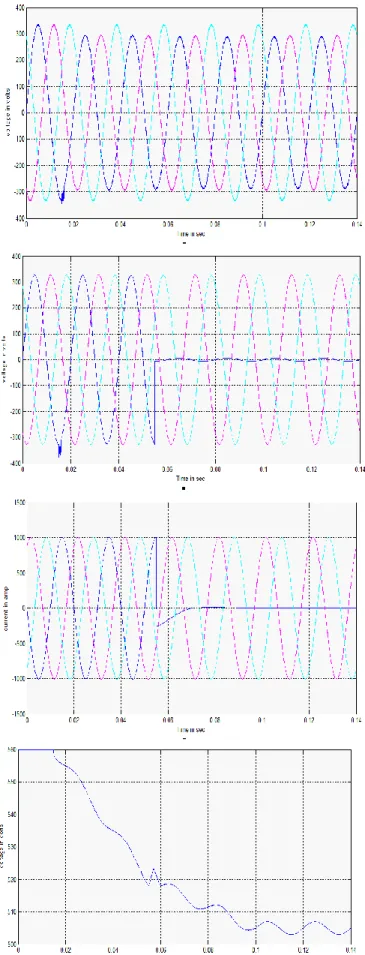
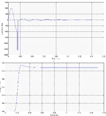
Fig 16. (a,c,e) Line current of phase-A and (b,d,f) dc-link voltage, for different initial values of the dc-link voltage, during down st ream phase-A-to-ground fault.
Fig. 16 shows the effect of lower initial dc-link voltage on the FCI operation during a phase-A to ground fault with the resistance of 0.05 at 10% length of the cable connecting bus 4 to bus 5 , at t=15 ms. If the DVR is inactive
(bypassed) during the fault, the fault current increases to about 7 times the rated load current. Fig. 16(a,c,e) shows that even under very low dc-link voltage conditions, the FCI control limits the fault current to less than the nominal load current in about one cycle. Fig. 16(b,d,f)
V. CONCLUSION . The study results conclude that:
The proposed multiloop control system provides a desirable transient response and steady-state performance effectively.
• The proposed control system detects and effectively interrupts the various downstream fault currents within two cycles (of 50 Hz);
• The proposed fault current interruption strategy limits the DVR dc-link voltage rise, caused by active power absorption, to restore the PCC voltage without interruption; in addition, it interrupts the downstream fault currents even under low dc-link voltage conditions.
• By using SVPWM technique the current ripples can be mitigated.
The proposed control system also performs satisfactorily under downstream arcing fault conditions.
18 ISSN: 2278 – 7798 All Rights Reserved © 2015 IJSETR
REFERENCES
[1]. Firouz Badrkhani Ajaei, Student Member, IEEE, Shahrokh Farhangi, and Reza Iravani, Fellow, IEEE Fault Current Interruption by the Dynamic Voltage Restorer IEEE transaction on power delivery,vol.28,apr 2013 [2]. N. G. Hingorani, ―Introducing custom power,‖ IEEE
Spectr., vol. 32, no. 6, pp. 41–48, Jun. 1995.
[3]. J. G. Nielsen, F. Blaabjerg, and N. Mohan, ―Control strategies for dynamic voltage restorer compensating voltage sags with phase jump,‖ in Proc. IEEE APEC’, 2001, pp. 1267–1273.
[4]. G. J. Li, X. P. Zhang, S. S. Choi, T. T. Lie, and Y. Z. Sun, ―Control strategy for dynamic voltage restorers to achieve minimum power injection without introducing sudden phase shift,‖ Inst. Eng. Technol. Gen. Transm. Distrib., vol. 1, no. 5, pp. 847–853, 2007.
[5]. S. S. Choi, B. H. Li, and D. M. Vilathga muwa, ―Design and analysis of the inverter-side filter used in the dynamic voltage restorer,‖ IEEE Trans. Power Del., vol. 17, no. 3, pp. 857–864, Jul. 2002.
[6]. B. H. Li, S. S. Choi, and D. M. Vilathga muwa, ―Design considerations on the line-side filter used in the dynamic voltage restorer,‖ Proc. Inst. Elect. Eng., Gen. Transm Distrib., vol. 148, no. 1, pp. 1–7, Jan. 2001.
[7]. S. S. Choi, B. H. Li, and D. M. Vilathgamuwa, Dynamic voltage restoration with minimumenergy injection,‖ IEEE Trans. Power. Syst., vol. 15, no. 1, pp. 51–57, Feb. 2000.
[8]. Y. W. Li, D.M. Vilathgamuwa, P. C. Loh, and F. Blaabjerg, ―A dualfunctional medium voltage level DVR to limit downstream fault currents,‖ IEEE Trans. Power. Electron., vol. 22, no. 4, pp. 1330–1340, Jul. 2007. [9]. Y. W. Li, D. M. Vilathgamuwa, F. Blaabjerg, and P. C.
Loh, ―A Robust control scheme for medium-voltage-level DVR implementation,‖ IEEE Trans. Ind. Electron., vol. 54, no. 4, pp. 2249–2261, Aug. 2007.
[10]. S. S. Choi, T. X. Wang, and D. M. Vilathgamuwa, ―A series compensator with fault current limiting function,‖ IEEE Trans. Power Del., vol. 20, no. 3, pp. 2248–2256, Jul. 2005.
[11]. B. Delfino, F. Fornari, and R. Procopio, ―An effective SSC control scheme for voltage sag compensation,‖ IEEE Trans. Power Del., vol. 20, no. 3, pp. 2100–2107, Jul. 2005.
[12]. C. Zhan, V. K. Ramachandara murthy, A.Arulampalam, C. Fitzer, S. Kromlidis, M. Barnes, and N. Jenkins, ―Dynamic voltage restorer based on voltage-space-vector PWM control,‖ IEEE Trans. Ind. Appl., vol. 37, no. 6, pp. 1855–1863, Nov./Dec. 2001.
[13]. D. M. Vilathga muwa, P. C. Loh, and Y. Li, ―Protection of microg rids during utility voltage sags,‖ IEEE Trans. Ind. Electron., vol. 53, no. 5, pp. 1427–1436, Oct. 2006. [14]. F. Badrkhani Ajaei, S. Afsharnia, A. Kahrobaeian, and
S. Farhangi ―A fast and effective control scheme for the dynamic voltage restorer,‖ IEEE Trans. Power Del., vol. 26, no. 4, pp. 2398–2406, Oct. 2011.
[15. ] M. S. Sachdev and M. A. Barlbeau, ―A new algorithm for digital impedance relays,‖ IEEE Trans. Power App., Syst., vol. PAS-98, no. 6, pp. 2232–2240, Nov./Dec. 1979.
[16]. S. R. Naidu and D. A. Fernandes, ―Dynamic voltage restorer based on a four-leg voltage source converter,‖ Inst. Eng. Technol. Gen. Transm Distrib., vol. 3, no. 5, pp. 437–447.
[17]. D. M. Vilathgamuwa, H. M. Wijekoon, and S. S. Choi, ―A novel technique to compensate voltage sags in multiline distribution system—The interline dynamic voltage restorer,‖ IEEE Trans. Ind. Electron., vol. 53, no. 5, pp. 1603–1611, Oct. 2006.
18]. D.M. Vilathgamuwa, A. A. D. R. Perera, and S. S. Choi, ―Voltage sag compensation with energy optimized dynamic voltage restorer,‖ IEEE Trans. Power Del., vol. 18, no. 3, pp. 928–936, Jul. 2003.
[19]. Y.W. Li, F. Blaabjerg, D. M. Vilathgamuwa, and P. C. Loh, ―Design and comparison of high performance stationary-frame controllers for DVR implementation,‖ IEEE Trans. Power. Electron., vol. 22, no. 2, pp. 602– 612, Mar. 2007.
[20]. B. Wang, G. Venkataramanan, and M. Illindala, Operation and control of a dynamic voltage restorer using transformer coupled H-bridge converters,‖ IEEE Trans. Ind. Electron., vol. 21, no. 4, pp. 1053–1061, Jul. 2006. [21]. H. Kim and S. Sul, ―Compensation voltage control in
dynamic voltage restorers by use of feed forward and state feedback scheme,‖ IEEE Trans. Power Electron., vol. 20, no. 5, pp. 1169–1177, Sep. 2005.
[22]. J. G. Nielsen, H. Nielsen, and F. Blaabjerg, ―Control and test of dynamic voltage restorer on the medium voltage grid,‖ in Proc. 38th Ind. Appl. Conf., Ind. Appl. Soc. Annu. Meeting, 2003, pp. 948–955.
[23]. M. J. Newman, D. G. Holmes, J. G. Nielsen, and F. Blaabjerg, ―A Dynamic Voltage Restorer (DVR) with selective harmonic compensation at medium voltage level,‖ IEEE Trans. Ind. Appl., vol. 41, no. 6, pp. 1744– 1753, Nov./Dec. 2005.
[24]. J. G. Nielsen, M. Newman, H. Nielsen, and F. Blaabjerg, Control and testing of a Dynamic Voltage Restorer (DVR) at medium voltage level,‖ IEEE Trans. Power. Electron., vol. 19, no. 3, pp. 806–813, May 2004. [25]. D.M.Vilathgamuwa, A. A. D. R. Perera, and S. S. Choi,
―Performance improvement of the dynamic voltage restorer with closed-loop load voltage and current-mode control,‖ IEEE Trans. Power. Electron., vol. 17, no. 5, pp. 824–834, Sep. 2002.
[26]. J. G. Nielsen and F. Blaabjerg, ―A detailed comparison of system topologies for dynamic voltage restorers,‖ IEEE Trans. Ind. Appl., vol. 41, no. 5, pp. 1272–1280, Sep./Oct. 2005.
[27]. P. Roncero-Sánchez, E. Acha, J. E. Ortega-Calderon, V. Feliu, and A. García- Cerrada, ―A versatile control scheme for a dynamic voltage restorer for power-quality improvement,‖ IEEE Trans. Power Del., vol. 24, no. 1, pp. 277–284, Jan. 2009.
[28]. P. Cheng, J. Chen, and C. Ni, ―Design of a state-feedback controller for series voltage-sag compensators,‖
19 ISSN: 2278 – 7798 All Rights Reserved © 2015 IJSETR
IEEE Trans. Ind. Appl., vol. 45, no. 1, pp. 260–267, Jan./Feb. 2009.
[29]. K. Tseng, Y.Wang, and D. M. Vilathgamuwa, ―An experimentally verified hybrid cassie-mayr electric arc model for power electronics simulations,‖ IEEE Trans. Power. Electron., vol. 12, no. 3, pp. 429–436, May 1997. [30]. A. Gaudreau and B. Koch, ―Evaluation of LV and MV
arc parameters,‖ IEEE Trans. Power Del., vol. 23, no. 1, pp. 487–492, Jan. 2008.