A Practical Approach to Layout versus Schematic
(LVS)
Swasti Pujari1, Smitha M R2, Amit Singh3, Mukul Anand4
1, 2, 3
Engineer, Einfochips Ltd. (An Arrow Company)
4
Technical Lead, Einfochips Ltd. (An Arrow Company)
Abstract: ASIC design implementation has become progressively complex and sophisticated with deep down the submicron technologies. Multiple processor cores, I/O s, several types of memories, analog circuits, and digital synthesized logic are being designed and implemented onto the same chip. Advanced IP integration proficiencies are needed to realize today's complex systems-on-chip designs and to keep up with the high demand in the semiconductor market. Ensuring product reliability to meet design goals and to achieve good yield is of significant and continuous concern.
Layout Versus Schematic (LVS) is process in the Chip Design and implementation that ensures if the layout (physical connectivity) of a specific Circuit matches with the actual Schematic (Circuit Diagram) of the design or not.
Keywords: LVS, Calibre, GDSII, Circuit Design, Schematic.
I. INTRODUCTION
Layout vs Schematic (LVS) check is performed in three basic steps:
1) Extraction: The tool takes GDSII file containing all the layers and uses polygon-based approach to determine the components like transistors, diodes, capacitors and resistors and also connectivity information between devices presented in the layout by their layers of construction. All the device layers, terminals of the devices, size of devices, nets, vias and the locations of pins are defined and given unique identification.
2) Reduction: All the defined information is extracted in the form of netlist.
3) Comparison: The extracted layout netlist is then compared to the netlist of the same stage using the LVS rule deck. In this stage the number of instances, nets and ports are compared. All the mismatches such as shorts and opens, pin mismatch etc. are reported. The tools also check topology and size mismatch.
A. Inputs for LVS
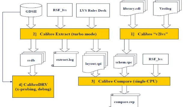
The following Design inputs are required for running LVS as depicted in Fig. 1.
1) Graphical Database System (GDS) layout database of the design
2) Schematic Netlist of the design
3) Cell definition file consisting of Intellectual property files and standard cells, Pad reference file.
[image:1.612.149.462.535.714.2]4) LVS rule deck: - a set of codes that is written in Standard Verification Rule Format (SVRF) or TCL Verification Format (TVF).
a) Step 1:- Generating Schematic spice Netlist (v2lvs)
i) LVS Comparison is done using SPICE Netlist format as shown in Fig. 2.
ii) Input: Verilog + CDL
iii) ‘v2lvs’ converts the Verilog into SPICE,
[image:2.612.245.370.139.247.2]iv) CDL Netlist will be added as INCLUDE.
Fig. 2. Generating Schematic spice Netlist
b) Step 2:- Extracting Layout data (GDS2SPICE)
i) LVS rules to extract connectivity is an input as shown in Fig. 3.
ii) PWR – GND detected at this stage.
iii) LVS ISOLATE SHORTS YES – This switch gives us the PWR- GND Shorts if any.
[image:2.612.202.425.353.471.2]iv) View with RVE as DRC database and fix it before LVS compare
Fig. 3. Extracting Layout data (GDS2SPICE)
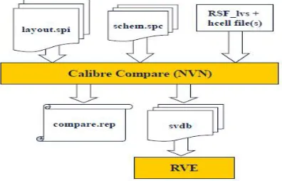
c) Step 3:- Comparing Schematic and Layout (NVN)
The Layout & Schematic SPICE files are compared and a report and below files are generated as the output as depicted in Fig. 4.
i) LVS.rep - Hierarchical LVS report
ii) SVDB (used by Calibre RVE) is a binary connectivity database containing all LVS information.
iii) LVS report - having the Schematic / Layout netlists.
iv) Contains the Probing / Cross probing information for all the nets.
[image:2.612.208.406.587.714.2]B. LVS output files 1) lvs.rep: ASCII
a) Summary of comparison results (CORRECT/INCORRECT)
b) Detailed cell based information
c) Device extraction, connect Information
d) Runtime, number of executed rules
2) lvs.rep.ext: ASCII
a) Label report
3) lvs.log: ASCII
a) Copy of used setup
b) Cell names/layer info
c) Rule deck commands, rules info
d) Hierarchy mod. Information (expand cell, flatten cell, …)
e) Comparison Information (device count, net count, …)
4) svdb: BINARY DB
a) Probing Database for RVE tool
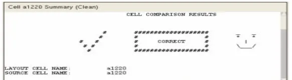
C. Calibre LVS report – Overview
1) Report format has two columns - LAYOUT :: SCHEMATIC
2) Header - gives a cell summary and reports CORRECT or INCORRECT
3) Hierarchical report
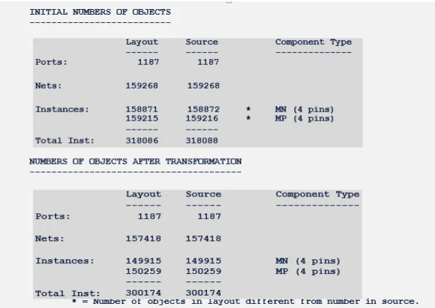
a) LVS information included for every cell
b) Devices/ports/nets BEFORE and AFTER transformation
c) Common error types are classified as follows:
i) Incorrect nets
ii) Incorrect instances
iii) Property errors
iv) Detailed instance connections
4) Use the detailed instance connections to debug the ERROR
a) Use layout coordinates to correlate with the netlist
[image:3.612.161.452.471.551.2]Fig. 5. Calibre LVS report – Overall comparison results
Fig. 7. Calibre LVS report – Transformation
Fig. 8 Calibre LVS report – Matching device summary
D. Calibre LVS Report – Correspondence points
1) Labels that correspond to netlist ports listed are here and all points should correspond.
2) Ports give Calibre a starting point for connectivity. It is important to first debug any ports that are mismatching, especially power/ground.
[image:4.612.118.481.80.513.2]E. Calibre LVS report – LVS Mismatches
The Typical LVS mismatches are as follows:
1) Different number of ports
2) Different number of nets
3) Connectivity errors
4) Cells with non-floating extra pins
5) Layout gate problems
6) Incorrect Supply nets
7) Property errors
8) Problems with Source netlist
F. Calibre LVS report - LVS Mismatch, summary 1) First of all, check the overall comparison results.
2) This will contain a summary of all LVS errors and warnings.
[image:5.612.147.460.502.607.2]3) Full error details appear later in the report.
Fig. 10. LVS Mismatch, summary
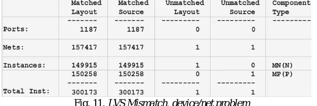
G. Calibre LVS report - LVS Mismatch, Device/net Problem
Check the device comparison statistics.
1) This section will detail exactly what type of devices are mismatching and by how many numbers.
2) The first priority is to check that the number of ports match.
3) If there is a mismatch of one or two ports and all N-types or P-types or all of both are mismatching, then it is likely that the power supply connections need to be debugged.
Fig. 11. LVS Mismatch, device/net problem
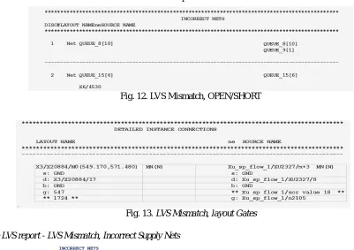
H. Calibre LVS report - LVS Mismatch, Open/Short 1) Discrepancy #1 - SHORT
a) Source nets “QUEUE_8[10]” & “QUEUE_9[1]” are shorted together in the layout to form the single layout net
“QUEUE_8[10]”.
2) Discrepancy #2 - OPEN
I. Calibre LVS report - LVS Mismatch, layout Gates
1) Debug Mismatched layout Gates first.
2) Look in the Detailed Instance Connections section of the report
[image:6.612.90.491.113.396.2]Fig. 12. LVS Mismatch, OPEN/SHORT
Fig. 13. LVS Mismatch, layout Gates
J. Calibre LVS report - LVS Mismatch, Incorrect Supply Nets
Fig. 14. LVS Mismatch, Incorrect Supply Nets
K. Calibre LVS report - LVS Mismatch, Property Errors
1) When Calibre extracts circuitry from the layout, it also extracts device size information.
2) Any device parameters that do not match the sizes specified in the netlist are listed in this section of the LVS report.
II. CALIBRELVSDEBUGGINGANDVERIFICATIONSMETHODS Many Debugging methods can be used to verify the LVS results:
A. LVS Black Boxing
B. Layout / Schematic Black Boxing
C. Short isolator (Short locator)
D. Layout/Schematic cross probing
E. Virtual connection
F. Exclude Cells
G. LVS report Options
H. Spice netlist Manipulation
I. [Spice netlist viewer]
III.LVSBLACKBOXING
1) Black boxing can filter out cells from the LVS
2) Connectivity is checked to the cell boundary and pins, inside not
3) The following options are set in the RSF file…
a) “LVS BOX “cell name” (Schematic black boxing) i) Full layout extraction is done first
ii) Black boxing works with schematic cell names
iii) Problems if shorts/stamping errors inside the cell (no clean netlist to use)
b) #Define Layout Box (Layout black boxing)
i) Enhancement to LVS BOX command
ii) Exclude full cell contents from LVS layout extraction, abstract kept
iii) That means block can truly be filtered and cell internal problems will not impact top level
iv) Very useful in case of shorts or stamping errors
v) Can also be used to debug hierarchical LVS errors
A. Short Isolator
1) “LVS Isolate Shorts yes By Layer” (rules)
2) “Hierarchical Short Isolation started” (log file)
3) “*.lvs.rep.shorts” is output (DRC type database)
4) Use CalibreRVE to graphically find the short location
5) RVE use different colours for each shorted net.• User could define which part of the short DB is related to which net, else the net part is defined as “unknown” (>=2008r01)
6) Watch the date stamp.
B. LVS cross Probing Using RVE
1) Calibre cross probing information is contained in the “SVDB” database
C. LVS Debugging methods – Others 1) Virtual Connect
a) Use Virtual connect command to get one step further, special for Supply shorts (limited usage for final verif.)
2) Exclude Cell
b) Remove cells complete from LVS run (for final verif. NOT ALLOWED)
3) LVS Report Options
a) Reduce/Enhance LVS report informations
b) E.g.: NOK option remove all CORRECT entries
4) Spice Netlist Manipulation
5) General Hints
a) make sure that LVS extraction of layout is clean first (OPEN/SHORT)
b) Power to Ground shorts errors must be fixed before Compare
REFERENCES
[1] ICCII User Guide.
[2] Calibre User Guide.
[3] https://en.wikipedia.org/wiki/Layout_Versus_Schematic
[4] EE5323 VLSI Design – https://www.people.ece.umn.edu