Electron Microscopy Studies of Non-Local Effects’ Impact
on Cathodoluminescence of Semiconductor Laser Structures
A. Czerwinski
*, M. P
ł
uska, J. Ratajczak, A. Szerling and J. Ka˛tcki
Institute of Electron Technology, Al. Lotnikow 32/46, 02-668 Warsaw, Poland
Spatially and spectrally resolved cathodoluminescence (CL) studies performed in a scanning electron microscope (SEM) or a scanning transmission electron microscope (STEM) are widely applied to determine the luminescence spectrum, map the optical activity and reveal defects in semiconductor structures. It is commonly recognized that the CL signal represents the local properties of the structure region excited by the electron beam. The present investigations show that if the structure under study contains regions with a strong electric field (e.g. p-n junction), the CL signal may much depend on phenomena far from the excitation region. The range of CL-results distortion extends from negligible changes to completely wrong output. It depends on various parameters described in the paper. The CL results obtained for AlGaAs/ GaAs laser heterostructures with InGaAs quantum well are presented. [doi:10.2320/matertrans.MB201007]
(Received August 25, 2010; Accepted January 7, 2011; Published February 16, 2011)
Keywords: cathodoluminescence (CL), semiconductor structure measurement
1. Introduction
Spatially and spectrally resolved cathodoluminescence (CL) studies performed in a scanning electron microscope (SEM) or a scanning transmission electron microscope (STEM) are widely applied to determine the luminescence spectrum, map the optical activity and reveal defects in semiconductor structures. It is commonly recognized that the CL signal represents the local properties of the structure region excited by the electron beam. The present investiga-tions aim to show that if the structure under investigation contains regions of a strong electric field (e.g. p-n junction), the CL signal may much depend on phenomena far from the excitation region.
The electron beam generates electron–hole (e–h) pairs in semiconductors. These pairs can diffuse randomly and recombine radiatively or nonradiatively. The photons emitted in the former case can be detected by a CL detector in a SEM or STEM microscope. The pairs would annihilate until all the excess carriers were eliminated. However, if an e-h pair is generated in or diffuses to a region of a strong electric field (e.g. the depletion region of a p-n junction), the electron and the hole may get separated. If both sides of the junction are connected by an external electric circuit, the electron beam induced current (EBIC,IEBIC) flows in this circuit.
The generation and outflow of EBIC current and the local recombination of e-h pairs are competing processes. Any e-h pair that recombines does not generate EBIC. On the other hand the separated pair that produces EBIC does not recombine at the e-beam placement. Thus, along with the EBIC increase the CL decreases.
But even if an external circuit does not exist (or is open), as typical in CL measurements, or a resistance load in the external circuit is significant, the e-h pair separation causes a forward bias between both sides of the junction. Because the e-beam spot is small, in the range of nanometers or micrometers, the e-beam in CL measurements excites only a small portion of the junction. The rest of the semiconductor
structure constitutes the nonlinear resistance parallel to the region of EBIC generation and also parallel to the external circuit (if it exists). Therefore, even without an external circuit the rest of the structure constitutes an internal load for theIEBICcurrent source.
This current always (even in the case of open-circuit configuration, i.e. without an external circuit) flows laterally from the place of the e-beam excitation through internal resistances (e.g. through resistive layers) towards the load, especially to the parts of the junction with higher conduc-tivity. Thus,IEBICmagnitude depends on phenomena present far from the excitation region, e.g. on the occurrence of defects and shunts. To sum up, the CL signal depends on non-local effects.1–4)
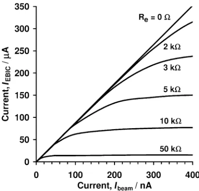
Dependence ofIEBICmeasured in an external circuit on the external load resistance is shown in Fig. 1.5) Not each increase of the resistance leads toIEBICreduction and to CL increase. For each structure the total resistance RT in the circuit can be defined as an equivalent resistance of all resistances (in internal and external circuits) connected to the source of the e-beam generated voltage. For lowRTtheIEBIC value is directly proportional to the e-beam current (Ibeam), i.e.IEBIC=Ibeamratio is constant.
On the contrary, whenRT is very high,IEBIC is very low, and CL is also almost independent of resistances. Beside these two cases of low and very high RT values, the CL intensity depends onRT components. In thisRT range, for a constantRT and a sufficientIbeam,IEBICincreases sublinearly with the increasing Ibeam. Such IEBIC dependence occurs because the potential drop on the overall load, i.e. the product IEBICRT, cannot increase above the finite value of the open-circuit voltage. It is similar to the photovoltaic effect in a photodiode. Also the power dissipated in the structure by this current cannot surpass the power of electrons accelerated by an electron gun.
If resistance in the external circuit is very low, EBIC in the internal circuit is negligible. When the load resistance in the external circuit enlarges, EBIC in the internal circuit increases as well. In an open-circuit configuration, the whole EBIC flows internally. Internal resistances are usually *Corresponding author, E-mail: [email protected]
significant, therefore the internal EBIC flow is smaller than the one measured in a short-circuit configuration, but it also suppresses CL. For example, CL measurements performed for structures with gold deposited on their facets (which represents a shunt short-circuiting p-n junction), show strong quenching of the CL signal generated in a quantum well, in comparison with the structures without gold.
CL measurements have been often performed for semi-conductor structures linked to an external electrical circuit. Sometimes the same specimens have been also analyzed by means of the EBIC technique.6,7) However, even if the CL spatial distribution was in previous articles somehow connected with the doping distribution or the impurity aggregation, it was related only to the local features in the close neighborhood of the pair-generation region. These local features were recombination lifetimes, densities of defects and impurities (e.g. deep levels, carrier traps, compositional inhomogeneities), local strains, etc.8–11)An impact of long-range or non-local effects on CL measurements has not been analyzed yet in works of other authors. It means that the non-local effects may have large impact on the CL signal while it is not recognized in investigations.
Such effects can be observed in many different CL measurements. The present authors discussed it in the works where the CL dependence on layer resistance was utilized for the measurement of thin-layer sheet resistance.1,4) The CL dependence on an e-beam current was also applied in the investigation of laser diode degradation,2)and for a signifi-cant improvement of the detection of defects in semi-conductor structures.3)
2. Experimental Procedure
In the present paper the CL results were obtained for AlGaAs/GaAs separate confinement heterostructure single quantum well (SCH SQW) ridge waveguide semiconductor
laser structures with InGaAs quantum well (QW). The structures, manufactured with Molecular Beam Epitaxy (MBE), were designed for a reliable high power continuous wave (CW) operation at the wavelength of 980 nm. The structures were grown on (100) GaAs conductive substrates with the sequence of layers as follows: nþ-type GaAs buffer, n-type emitter AlGaAs:Si, the active layer of 8 nm InGaAs quantum well embedded in the middle of two undoped GaAs waveguides 300 nm thick, p-type emitter AlGaAs:Be, and low resistivity GaAs:Be pþsub-contact cap layer.12)
An overflow of the laser current outside the narrow lasing region is reduced by the formation of a mesa. The thinning (etching) of the p-AlGaAs cladding on both sides of the mesa increases its resistance so that the etched regions become the lateral confinements. The mesa is covered by metallisation, which produces an ohmic contact to the thin p+ sub-contact layer. The second ohmic contact is on the structure backside. The semiconductor layers of the mesa and outside the mesa are shown in Fig. 2(a). The corre-sponding electrical diagram related to the e-beam excitement in the region outside the mesa (as performed for the investigated structures, with CL results presented in Figs. 3 and 4) is seen in Fig. 2(b). This diagram presents the internal and external current loops in the structure with schematically drawn: the source of EBIC current, lateral (linear) internal resistances of the upper (cladding) layer (Rs), non-linear internal resistances of the p-n junction (Rj) and the resistance in an external circuit (Re). Only lateral resistances of thinned upper p-type cladding (in the lateral confinement region) are marked, because in this structure they are much larger than resistances of the thick n-type (bottom) layers. For the CL results shown in Fig. 4 the e-beam was placed at the mesa region.
The MonoCL2 (Oxford Instruments) system in Philips XL30 SEM with LaB6 electron gun was used for the CL
detection. All CL spectra were taken from a small area of specimen. The CL spatial distribution was approximately uniform across the whole surface. Once the measured area was selected, there were no stage or probe (i.e. scanned area) movements until all CL spectra were registered.
3. Results and Discussion
An impact of non-local effects is clearly visible consid-ering a wide spectrum of the CL signal containing several Fig. 1 An exemplary experimental dependence ofIEBICin AlGaAs/GaAs
heterostructure with an InGaAs quantum-well semiconductor structure (at the mesa region) on the e-beam currentIbeam, measured at various constant external resistancesRe. The beam energyEbeam¼30keV and linear ratio IEBIC=Ibeam¼880 at the low Ibeam range (whose ratio is different for various samples).
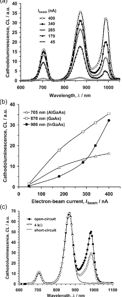
[image:2.595.65.270.70.266.2] [image:2.595.306.547.74.183.2]peaks, which correspond to the emission of the CL signal from different layers. Figure 3(a) shows a spectrum meas-ured in the wavelength range 600–1100 nm for variousIbeam. The CL peaks at 705, 870 and 980 nm correspond respec-tively to the excitations in AlGaAs, GaAs and InGaAs layers. Along with the Ibeam change, the magnitudes of these CL
peaks change as well (Fig. 3(b)), while their wavelengths shift negligible even at highIbeam.
An analysis of the results shown in Fig. 3(b) reveals that the relationship between the CL intensity Ibeam is highly dependent on the existence of a strong electric field in the region or layer where the corresponding CL wavelength is emitted.
Fig. 3 (a) The CL spectra for AlGaAs/GaAs heterostructure with an InGaAs quantum well, measured atEbeam¼30keV andIbeam¼45, 179, 285, 340 and 400 nA. (b) The magnitudes of CL peaks at differentIbeam values. The peaks at 705, 870 and 980 nm wavelengths correspond to the excitation in the AlGaAs, GaAs and InGaAs layers, respectively. (c) The CL spectra measured at Ebeam¼30keV and Ibeam¼259nA in the conditions of an open-circuit, a short-circuit and in the case of a changeable resistance with an intermediate value (4 khere) included in the external circuit.
[image:3.595.317.530.71.570.2] [image:3.595.63.277.77.597.2]For the peaks related to GaAs and AlGaAs layers, after reaching a certain CL quantity the further CL increase is linear withIbeam. However, for the peak corresponding to the quantum well the CL increase is superlinear.
The structure of laser diode is designed to assure the recombination of carriers within the active region. For this purpose the very thin low-bandgap InGaAs layer is sand-wiched between two high-bandgap layers in the middle of the p-n junction. Simultaneously, a strong electric field exists within the p-n junction. Therefore, when the diode is excited by the e-beam, EBIC is generated intensively in the InGaAs layer. The quantity of the separated e-h pairs depends on the electric field strength and on the width of the p-n junction depletion region.
WhenIbeamcurrent generatesIEBIC,IEBICoutflow is either easy (i.e. the effective resistance of all internal and external electrical circuits is small) or difficult (i.e. the effective resistance is significant or large). In the latter case, some generated carriers cannot outflow (see Fig. 1) and they compensate the electric field, which leads to smaller separation, smaller EBIC and higher CL. Thus, in such cases the magnitude of the related CL peak increases superlinearly with theIbeamincrease.
This dependence of the CL signal on the feasibility of EBIC outflow is seen in Fig. 3(c). The three CL spectra were measured for the same structure and in the same wavelength range 600–1100 nm, but in different conditions regarding the outflow. In comparison, Fig. 3(a) shows the CL spectrum only in open-circuit conditions, when the EBIC outflow is the most difficult and CL signal is the largest.
One of the CL spectra in Fig. 3(c) was measured in short-circuit conditions in an external short-circuit. It reveals that no CL signal is measured for wavelengths related to the excitation in a quantum well. This effect means that (1) in the strong electric field of the p-n junction all e-h pairs generated by the e-beam are separated, and (2) in short-circuit conditions all the separated e-h pairs outflow. Only if the EBIC outflow is more difficult, a CL signal can be observable, as in the case of the changeable resistance with intermediate value included in the external circuit or in open-circuit conditions.
Thus, a wrong conclusion from CL investigations may be drawn due to non-local effects when the observable local CL values are low. Such a region may be misinterpreted as a region of defects and high nonradiative recombination. In fact, it can be a region without strong defects, but with an easy outflow of EBIC to either an external circuit or a site of a locally increased forward current of the p-n junction. Next, when the distance between the scanned e-beam and the defected site enlarges, the enhancement of detected CL may be misinterpreted as less affected by the local defectivity.
The dependence of the CL measurement results on external resistances, especially when an e-beam is placed outside the mesa, is an evident proof of an impact of non-local effects. Moreover, because the total resistance depends on resistances in external and internal circuits, the CL changes due to the presence of various external resistances are analogous to the changes in the presence of various shorts and defects within the structure. A low resistance of a
short-circuit in the first approximation is analogous to a shunt, while intermediate values of external resistances are analo-gous e.g. to defects in a p-n junction linked with an excitation region by lateral conductive paths of layers. These lateral resistances depend on their sheet resistance and width, and on the distance between the e-beam and the site. The p-type cladding above the junction, if being etched to form thin lateral confinements, constitutes much higher lateral resist-ance to each place where a local EBIC component flows through the junction than the resistance of a lateral path below the junction. Therefore, while open-circuit conditions lead to an impact on CL of the defects present in the internal circuit, the changeable resistance in the external circuit additionally quenches CL (in comparison to the open-circuit case) as if an additional defect was present somewhere in the internal circuit. In cases when the lateral resistance of conductive paths (whose resistance is usually linear) is the main component of the total resistance of circuits, the EBIC outflow is proportional to the forward bias. However, in these cases the bias decreases along paths, i.e. with the increasing distance from the e-beam. When the forward bias, which is applied to a p-n junction decreases, the non-linear resistance of this junction increases. Therefore, beyond a certain distance to an e-beam, it is the junction resistance that limits the EBIC flow, not the resistance of lateral path towards the site.
Figure 3(c) shows additionally that magnitudes of CL peaks are often negligible at the low Ibeam and become distinguishable from the background CL noise only at a higherIbeam. This phenomenon also may depend strongly on non-local effects, because in an adequately low Ibeamrange the non-linear resistance of junctions is high comparatively to the lateral resistances of layers. Thus, all the junction sites are equally accessible and EBIC flows practically all over the structure, regardless of the structure size. Then each junction current, especially at shunts or defects in the structure, affects and quenches the CL signal.
Another wrong conclusion may occur at range of even biggerIbeamvalues, i.e. when CL signal is already observable. Because in each site of structure the detected CL is affected by the current flow all over the structure, therefore no CL contrast can be revealed between the truly locally defected areas and any other point of the structure. On the contrary, for high Ibeam (i.e. high IEBIC) values the junction resistance decreases. Lateral resistances between e-beam and remote defects become dominant, therefore distant shunts or defects much less affect CL (as if effective area of the investigated structure being diminished) and the contrast due to local defectivity becomes visible.
contrary, even in these cases an increase inIbeam value may prevent the quenching of the CL-signal.
To sum up, the IEBIC current flow decreases the CL intensity. This current may outflow through ohmic contacts into an external circuit or may flow through the internal shorts/loops of the structure. In the latter case, such a flow through the junction can be spatially nonuniform, with the most of the current flowing from the top of the structure to the bottom in one or several specific leakage points.
The superlinear increase of CL with Ibeam, as seen in Fig. 3(b) for the peak related to the quantum well, can be related to two factors. Firstly, it is shown in Fig. 1 that at sufficientIbeam,IEBICincreases sublinearly with the increas-ingIbeam, leading to the superlinear increase of CL. Secondly, the Ibeam increase —when lateral resistances become domi-nant— leads to the above described narrowing of an effective area responsible for the CL quenching, i.e. to the lowering of the defects quantity strongly affecting CL. It gives the additional reason for the superlinear CL increase.
To confirm that both the above-mentioned reasons of superlinear CL enhancement are independent, CL was measured also on structures with the p-type AlGaAs claddings entirely removed (by deep etching) outside the mesa region. Only the first reason superlinear CL increase occurs then, because for such structures the quantity of defects affecting CL is independent of Ibeam. Namely, the EBIC outflow into lateral confinements is absent, while the outflow into the mesa region occurs along the low resistivity pþ sub-contact cap layer and metallization, i.e. the lateral resistance in this region is so low that the second reason vanishes.
But the first reason alone still causes the superlinear increase of CL peak, which corresponds to the InGaAs quantum well, with the increasing Ibeam (Figs. 4(a), (b)). Figure 4(a) shows the CL spectrum measured for a wider range ofIbeamvalues than in Fig. 3. Figure 4(b) presents the dependence of the CL peak magnitudes onIbeam. In that case for higher Ibeam values the superlinear CL increase with increasing Ibeam is revealed not only for the CL peak corresponding to the InGaAs quantum well but also for the peak related to GaAs layers.
Such dependence of the CL signal for GaAs layers can be also related to the EBIC generation in a strong field of the p-n junction, in which case the EBIC magnitude increases sublinearly withIbeam. Although there is no strong field that could separate e-h pairs in thick GaAs layers at the bottom of the structure, the active region contains an InGaAs quantum well embedded between two undoped thin GaAs waveguides. The e-h pairs excited in these GaAs waveguides can be separated in a strong electric field present in the active region. Therefore, they undergo the same impacts of non-local effects as the pairs generated in the InGaAs layer.
This impact is confirmed qualitatively in Fig. 4(c) in the cases of an open-circuit, a short-circuit and with an additional resistance in an external circuit. For high Ibeam values the short-circuit conditions not only entirely remove the InGaAs-related CL peak but also partially diminish the GaAs-related peak. It is diminished also at measurements with an additional resistance in the external circuit. Thus,
defects and shunts impact CL also for the GaAs-related peak at this Ibeam range. As in the case of the e-h pairs generated in InGaAs, also these generated in the GaAs waveguides give a component of the CL signal, which diminishes to zero in short-circuit conditions. The rest of the CL signal at the wavelength equal to 870 nm, i.e. the part, which is not removed in short-circuit conditions, shows the linear dependence on Ibeam. It confirms that two CL components from GaAs layers exist. One component is present for all Ibeam and therefore can be related to thick GaAs layers, in which e-h pairs are not separated due to an electric field. The second CL component originates from much thinner layers than the first one, therefore it is invisible at a lowerIbeam. However, because this component strongly increases withIbeam, it becomes clearly visible in the range of highIbeam.
The ratio of both CL components, the first related respectively to doped thick GaAs bottom layers and the second —to thin undoped GaAs waveguides, depends also on the e-beam energy. Therefore, under other conditions (as well as for another sample), the ratio of the both CL components may be different, thus the superlinear increase of CL may be revealed for the GaAs-related peak even at a much lower Ibeam.
Figure 4(b) shows that CL peak magnitudes for the InGaAs-related peak measured for a wider range of Ibeam values than in Fig. 3 become linearly increasing with large values ofIbeam. It is caused by the fact thatIEBICat such large Ibeam becomes almost constant (see Fig. 1). Thus the above mentioned first reason of the superlinear CL enhancement disappears, while the second reason vanishes in this type of structure, as it was explained above.
4. Conclusions
It is commonly recognized that the CL signal represents the local properties of the structure region excited by the electron beam. However, the present investigations show that in the structures with strong electric field (e.g. p-n junction) the CL signal may much depend on phenomena far from the excitation region. As it was described, in this case the CL results depend on the value of e-beam current, the resistance distribution within the structure and the external resistance connected to the structure. Therefore, the range of CL-results distortion extends from negligible changes to completely wrong output. In order to estimate the distortion and take it into consideration when analysing CL results, various values of e-beam current should be applied in CL measurements.
REFERENCES
1) A. Czerwinski, M. Pluska, J. Ratajczak, A. Szerling and J. Ka˛tcki: Appl. Phys. Lett.93(2008) 041109-1-3.
2) M. Pluska, A. Czerwinski, J. Ratajczak, A. Szerling and J. Ka˛tcki: J. Microscopy236(2009) 137–142.
3) M. Pluska, A. Czerwinski, J. Ratajczak, A. Szerling and J. Ka˛tcki: Acta Phys. Polonica A116(2009) S86–S88.
4) A. Czerwinski, M. Pluska, J. Ratajczak, A. Szerling and J. Ka˛tcki: J. Microscopy237(2010) 304–307.
Mater. Trans.48(2007) 949–953.
6) K. A. Record, D. R. Palmieri, N. M. Haegel and D. Wynne: Appl. Phys. Lett.75(1999) 3829–3831.
7) E. B. Yakimov, P. S. Vergeles, A. Y. Polyakov, N. B. Smirnov, A. V. Govorkov, I.-H. Lee, C. Ro Lee and S. J. Pearton: Appl. Phys. Lett.90
(2007) 152114-1-3.
8) A. Gustafsson, M.-E. Pistol, L. Montelius and L. Samuelson: J. Appl. Phys.84(1998) 1715–1775.
9) N. M. Haegel, J. D. Fabbri and M. P. Coleman: Appl. Phys. Lett.84
(2004) 1329–1331.
10) H. P. Strunk, M. Albrecht and H. Scheel: J. Microscopy224(2006) 79– 85.
11) C. Diaz-Guerra, J. Vincent, J. Piqueras and E. Dieguez: J. Phys. D: Appl. Phys.40(2007) 137–143.