Motorola reserves the right to make changes without further notice to any products herein to improve reliability, function or design. Motorola does not assume any liability arising out of the application or use of any product or circuit described herein; neither does it convey any license under its patent rights nor the rights of others. Motorola products are not designed, intended, or authorized for use as components in systems intended for surgical implant into the body, or other applications intended to support or sustain life, or for any other application in which the failure of the Motorola product could create a situation where personal injury or death may occur. Should Buyer purchase or use Motorola products for any such unintended or unauthorized application, Buyer shall indemnify and hold Motorola and its officers, employees, subsidiaries, affiliates, and distributors harmless against all claims, costs, damages, and expenses, and reasonable attorney fees arising out of, directly or indirectly, any claim of personal injury or death associated with such unintended or unauthorized use, even if such claim alleges that Motorola was negligent regarding the design or manufacture of the part.
1
OSC
Block User Guide
V02.03
Original Release Date: 19 July 2002 Revised: 12 February 2003
OSC Block User Guide — V02.03 2
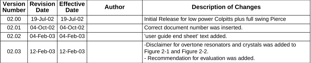
Revision History
Version Number Revision Date EffectiveDate Author Description of Changes
02.00 19-Jul-02 19-Jul-02 Initial Release for low power Colpitts plus full swing Pierce 02.01 04-Oct-02 04-Oct-02 Correct document number was inserted.
02.02 04-Feb-03 04-Feb-03 ’user guide end sheet’ text added.
02.03 12-Feb-03 12-Feb-03
[image:2.595.45.551.142.245.2]-Disclaimer for overtone resonators and crystals was added to Figure 2-1 and Figure 2-2.
3
Table of Contents
Section 1 Introduction
1.1 Overview. . . .9
1.2 Features . . . .9
1.3 Modes of Operation . . . .9
Section 2 Signal Description
2.1 Overview. . . .112.2 Detailed Signal Descriptions. . . .11
2.2.1 VDDPLL, VSSPLL . . . .11
2.2.2 EXTAL, XTAL. . . .11
2.2.3 XCLKS . . . .12
Section 3 Memory Map and Registers
Section 4 Functional Description
4.1 General. . . .154.2 Amplitude Limitation Control (ALC) . . . .15
4.3 Clock Monitor (CM). . . .15
OSC Block User Guide — V02.03
5
List of Figures
OSC Block User Guide — V02.03
7
List of Tables
OSC Block User Guide — V02.03
9
Section 1 Introduction
1.1 Overview
The OSC module provides two alternative oscillator concepts:
1. a low noise and low power Colpitts oscillator with amplitude limitation control (ALC).
2. a robust full swing Pierce oscillator with the possibility to feed in an external square wave.
1.2 Features
The Colpitts OSC option provides the following features:
• Amplitude Limitation Control (ALC) Loop:
– low power consumption and low current induced RF emission.
– sinusoidal waveform with low RF emission.
– low crystal stress. An external damping resistor is not required.
– normal and low amplitude mode for further reduction of power and emission.
• an external biasing resistor is not required.
The Pierce OSC option provides the following features:
• wider high frequency operation range.
• no DC voltage applied across the crystal.
• full rail-to-rail (2.5V nominal) swing oscillation with low EM susceptibility.
• fast start up.
Common features:
• clock monitor (CM).
• operation from the VDDPLL 2.5 V (nominal) supply rail.
1.3 Modes of Operation
Two modes of operation exist:
• amplitude limitation controlled Colpitts oscillator mode suitable for power and emission critical applications.
OSC Block User Guide — V02.03
11
Section 2 Signal Description
2.1 Overview
This section lists and describes the signals that connect off chip.
2.2 Detailed Signal Descriptions
2.2.1 VDDPLL, VSSPLL
These pins provide the operating voltage (VDDPLL) and ground (VSSPLL) for the OSC circuitry. This allows the supply voltage to the OSC to be independently bypassed.
2.2.2 EXTAL, XTAL
These pins provide the interface for either a crystal or a CMOS compatible clock to control the internal clock generator circuitry. EXTAL is the external clock input or the input to the crystal oscillator amplifier. XTAL is the output of the crystal oscillator amplifier. All the MCU internal system clocks are derived from the EXTAL input frequency. In Full Stop Mode (PSTP=0) the EXTAL pin is pulled down by an internal resistor of typical 200k Ohms.
NOTE: Motorola recommends an evaluation of the application board and chosen resonator or crystal by the resonator or crystal supplier!
NOTE: Crystal circuit is changed from standard!
[image:11.595.192.465.476.597.2]Colpitts circuit is not suited for overtone resonators and crystals!
Figure 2-1 Colpitts Oscillator Connections (XCLKS=0) MCU C2 EXTAL XTAL Crystal or VSSPLL ceramic resonator C1
CDC*
* Due to the nature of a translated ground Colpitts oscillator a DC voltage bias is applied to the crystal
OSC Block User Guide — V02.03
12
[image:12.595.192.452.104.219.2]NOTE: Pierce circuit is not suited for overtone resonators and crystals without a careful component selection!
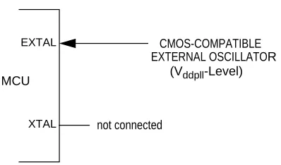
[image:12.595.192.391.340.457.2]Figure 2-2 Pierce Oscillator Connections (XCLKS=1)
Figure 2-3 External Clock Connections (XCLKS=1)
2.2.3 XCLKS
The XCLKS is an input signal which controls whether a crystal in combination with the internal Colpitts (low power) oscillator is used or whether Pierce oscillator/external clock circuitry is used. The XCLKS signal is sampled during reset with the rising edge of RESET.Table 2-1 lists the state coding of the sampled XCLKS signal. Refer to device specification for polarity of the XCLKS pin.
Table 2-1 Clock Selection Based on XCLKS
XCLKS Description
0 Colpitts Oscillator selected
1 Pierce Oscillator/external clock selected MCU
EXTAL
XTAL
RS* RB VSSPLL Crystal or ceramic resonator C4 C3
* Rs can be zero (shorted) when used with higher frequency crystals. Refer to manufacturer’s data.
MCU EXTAL XTAL CMOS-COMPATIBLE EXTERNAL OSCILLATOR not connected
13
Section 3 Memory Map and Registers
OSC Block User Guide — V02.03
15
Section 4 Functional Description
4.1 General
The OSC block has two external pins, EXTAL and XTAL. The oscillator input pin, EXTAL, is intended to be connected to either a crystal or an external clock source. The selection of Colpitts oscillator or Pierce Oscillator/external clock depends on the XCLKS signal which is sampled during reset. The XTAL pin is an output signal that provides crystal circuit feedback.
A buffered EXTAL signal, OSCCLK, becomes the internal reference clock. To improve noise immunity, the oscillator is powered by the VDDPLL and VSSPLL power supply pins.
The Pierce oscillator can be used for higher frequencies compared to the low power Colpitts oscillator.
4.2 Amplitude Limitation Control (ALC)
The Colpitts oscillator is equipped with a feedback system which does not waste current by generating harmonics. Its configuration is “Colpitts oscillator with translated ground”. The transconductor used is driven by a current source under the control of a peak detector which will measure the amplitude of the AC signal appearing on EXTAL node in order to implement an Amplitude Limitation Control (ALC) loop. The ALC loop is in charge of reducing the quiescent current in the transconductor as a result of an increase in the oscillation amplitude. The oscillation amplitude can be limited to two values. The normal amplitude which is intended for non power saving modes and a small amplitude which is intended for low power operation modes. Please refer to the CRG block user guide for the control and assignment of the amplitude value to operation modes.
4.3 Clock Monitor (CM)
OSC Block User Guide — V02.03
17
Section 5 Interrupts
OSC Block User Guide — V02.03
19
OSC Block User Guide — V02.03
20