Memristive operation mode of a site-controlled quantum dot floating gate transistor
P. Maier, F. Hartmann, T. Mauder, M. Emmerling, C. Schneider, M. Kamp, S. Höfling, and L. Worschech
Citation: Applied Physics Letters 106, 203501 (2015); doi: 10.1063/1.4921061
View online: http://dx.doi.org/10.1063/1.4921061
View Table of Contents: http://scitation.aip.org/content/aip/journal/apl/106/20?ver=pdfcov
Published by the AIP Publishing
Articles you may be interested in
Charging dynamics of a floating gate transistor with site-controlled quantum dots Appl. Phys. Lett. 105, 053502 (2014); 10.1063/1.4892355
Exciton and multiexciton optical properties of single InAs/GaAs site-controlled quantum dots Appl. Phys. Lett. 103, 183112 (2013); 10.1063/1.4828352
Photocurrent spectroscopy of site-controlled pyramidal quantum dots Appl. Phys. Lett. 101, 031110 (2012); 10.1063/1.4737426
Single photon emission from site-controlled pyramidal quantum dots Appl. Phys. Lett. 84, 648 (2004); 10.1063/1.1643533
Optical control of charge number in single floating quantum-dot gate in field-effect transistor structure Appl. Phys. Lett. 78, 1930 (2001); 10.1063/1.1359139
Memristive operation mode of a site-controlled quantum dot floating gate
transistor
P.Maier,1,a)F.Hartmann,1T.Mauder,1M.Emmerling,1C.Schneider,1M.Kamp,1
S.Hofling,€ 1,2and L.Worschech1
1
Technische Physik, Physikalisches Institut, Wilhelm Conrad Rontgen Research Center for Complex Material€
Systems, Universitat W€ urzburg, Am Hubland, D-97074 W€ €urzburg, Germany
2
SUPA, School of Physics and Astronomy, University of St Andrews, St Andrews KY16 9SS, United Kingdom
(Received 9 March 2015; accepted 2 April 2015; published online 18 May 2015)
We have realized a floating gate transistor based on a GaAs/AlGaAs heterostructure with site-controlled InAs quantum dots. By short-circuiting the source contact with the lateral gates and per-forming closed voltage sweep cycles, we observe a memristive operation mode with pinched hys-teresis loops and two clearly distinguishable conductive states. The conductance depends on the quantum dot charge which can be altered in a controllable manner by the voltage value and time interval spent in the charging region. The quantum dot memristor has the potential to realize artifi-cial synapses in a state-of-the-art opto-electronic semiconductor platform by charge localization and Coulomb coupling.VC 2015 AIP Publishing LLC. [http://dx.doi.org/10.1063/1.4921061]
In 1971, Chua postulated the existence of a fourth fun-damental circuit element beside the capacitor, inductor, and resistor.1,2 This circuit element, now known as memristor, combines the functionality of a switchable resistor (transis-tor) with memory. Since the pioneering work by Strukov
et al. in 2008,3which described resistance switching in thin TiO2layers with oxygen deficient with a memristive model, memristive switching has been identified in various material systems including oxide films,4–6silver compounds,7,8spin memristive systems,9 and floating-gate transistors.10,11 Memristors are characterized by a pinched hysteresis loop with a state and time dependent resistance or conductance which depends on the previous charge flow through the de-vice.1–3This state-dependent conductance enables memris-tors to emulate artificially the functionality of synapses,12,13 the connections between neurons in neural networks. The strength of these connections can be tuned dynamically depending on the time difference of pre- and post-synaptic pulses,14,15 a crucial scheme for learning in neural net-works.16,17 Artificial synapses are key building blocks in brain-inspired, non-von Neumann architectures with a paral-lel computing scheme which can for instance be used to implement multiobject detection and classification.18
Here, we demonstrate a memristive operation mode of a quantum dot (QD) floating gate transistor by short-circuiting the source contact of the quantum wire (QW) and lateral gates. The memristive operation mode appears due to the Coulomb interaction of QD localized charges with the nearby QW, which leads in one sweep direction of the volt-age to a smaller and in the other sweep direction to a larger conductance. We also examined the amount of QD-localized charges which can be controlled via the charging voltage or the time interval spent in the charging region. The memris-tive operation mode is observed up to temperatures of 165 K. The application of rectangular voltage pulses to the source
and drain contacts of the device allows to tune the conduct-ance in dependence on the time difference of the pulses. This mimics the increase (potentiation) and decrease (depression) of synaptic strength between two neurons by changing the relative timing of pre- and post-synaptic pulses.
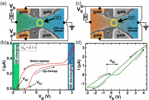
Fig. 1(a) depicts an electron microscope image of the studied device. A GaAs/AlGaAs heterostructure was grown by molecular beam epitaxy, forming a two-dimensional elec-tron gas (2DEG) 90 nm below the surface. Precise position-ing of the InAs QDs was realized by a growth step with InAs after defining a regular pattern of 50 nm deep nanoholes. The whole structure was covered with a GaAs layer. Lateral gates
FIG. 1. (a) Electron microscope image of the device and circuit diagram for the floating gate operation mode. The dark contrasts indicate the positions of the QDs and the etched trenches which electrically isolate the quantum wire from the lateral gates. The lateral gates and the QW are connected to the gate voltageVgand the bias voltageVb, respectively. A yellow circle high-lights the QD in the center of the QW. (b)I-Vg-characteristic in the floating gate operation mode. The arrows indicate the sweep cycle directions as well as the corresponding threshold voltagesVtdandVtu. (c) Circuit diagram to realize the memristive operation mode. The bias voltageVbis applied simul-taneously to the top contact of the QW and the lateral gates. An additional resistance with 1 MXis used in series to the QW. (d)I-Vb-characteristic in the memristive operation mode. A pinched hysteresis loop with a widthVth of the low conductive state is observed.
a)Author to whom correspondence should be addressed. Electronic mail: [email protected].
0003-6951/2015/106(20)/203501/4/$30.00 106, 203501-1 VC2015 AIP Publishing LLC
[image:2.612.315.560.450.614.2]and a quantum wire structure were realized by electron beam lithography and dry chemical etching. The dark contrast in the electron microscope image indicates the positions of the QDs and the etched trenches to electrically isolate the gates from the QW. A more detailed description of the growth and positioning techniques is given in Refs.19and20.
The device can be operated in two operation modes: the floating gate mode and the memristive mode. Fig.1(a) dis-plays the circuit diagram in the floating gate operation mode. For this purpose, a constant bias voltageVbwas applied to the left contact of the QW (source) while a gate voltageVg was applied to the lateral gates. The right contact of the QW (drain) is used as common ground. The currentIwas deter-mined as voltage drop across a resistor with 10 kXin series to the QW. If not stated differently, the measurements were conducted at 4.2 K in the dark. Fig.1(b)shows theI-Vg char-acteristic of the device in floating gate operation mode. The gate voltage was swept with a rate ofDVg/Dt¼0.2 V/s from 2.0 to 4.0 V (up-sweep direction) and back (down-sweep direction), and the bias voltage was set constantly to
Vb¼0.1 V. The arrows indicate the gate voltage sweep cycle directions and the corresponding threshold voltagesVtuand
Vtdfor the up- and down-sweep direction, respectively. For small gate voltages, the QW is depleted and the QD becomes charged.20,21 After exceeding Vtu, the current increases monotonically.Vtudepends on the number of QD localized charges and the capacitive couplings between the gate, the QD, and the QW.22,23The QD becomes discharged for large gate voltages, leading to an enhanced current and a smaller threshold voltage during the down-sweep direction. The ap-proximate gate voltage ranges for charging and discharging the QD are indicated by the shaded regions in Fig.1(b).
In the memristive operation mode, the bias voltage was applied simultaneously to the source contact of the QW and the lateral gates (see Fig.1(c)). An additional resistance with 1 MXis connected in series to the channel. TheI-Vb charac-teristic in the memristive operation mode is depicted in Fig.
1(d). The voltage was swept between 4.6 V and the minimum value Vbm¼ 3.0 V. A pinched hysteresis loop, the finger print of memristors,1,2is observed. The differential conduct-ance around zero bias voltage is 0.7lS for the down- and almost zero for the up-sweep direction. Charging of the QD occurs for Vb<1.9 V (almost zero differential conduct-ance) which corresponds to the charging region in the float-ing gate operation mode. The Coulomb interaction of QD localized charges with the QW results in the low conductive state with almost zero conductance. The current increase at 3.8 V is attributed to a discharging of the QD. We observe that the voltage ranges for charging and discharging differ from sample to sample because of varying geometries and quantum dot positions leading to small deviations in the current-voltage characteristic and pinched hysteresis loop.
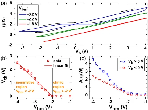
Fig. 2(a) shows current-voltage-characteristics con-ducted in the memristive operation mode for differentVbm. No pinched hysteresis loop is observed above1.8 V. For smallerVbm(2.2 and3.2 V), two distinguishable conduc-tive states (low and high) around zero bias are clearly evi-dent. The widths of the low conductive states are 0.1 and 1.7 V. They can be related to the voltageVtuof the current-onset in the floating gate operation mode with Vth2Vtu.
Fig.2(b)shows the plateau width versusVbm. It remains zero above (ohmic response) and increases almost linearly below 2.0 V (memristive response). We attribute this linear shift to the threshold voltage shift DVtu¼Dnq/Ceff of a floating gate transistor in close vicinity to a QD.22 Here, Dnis the shift of the number of localized charges,qis the elementary charge, andCeffaccounts for the effective capacitive coupling between the QD, the 2DEG, and the gate. In the memristive operation mode, charging of the QD occurs for Vb<1.9 V and thus Dn is determined by Dn¼(1.9 VVbm)/DV with DV being the voltage difference to charge the QD with one additional electron. Dn is only defined for Vbm1.9 V. For largerVbm, the QD is not charged and we observe linear cur-rent-voltage-characteristics (ohmic response). SinceVth2Vtu, the width of the low conductive state is
Vth 2q
DV Cef f
1:9VVbm
ð Þ: (1)
The data in Fig. 2(b)were fitted according to Eq.(1)with a shift ofDVCeff0.281018C. The memristive opera-tion mode can also be analyzed by means of the area A, which is enclosed by the pinched hysteresis loop. Fig. 2(c)
shows Afor positive and negative bias voltages versusVbm. Similar to the plateau width, A is almost zero above but increases linearly below 2.0 V. BothVthandA depend on the shape of the pinched hysteresis loop, which correlates to the constitutive relation of the memristor (ideal memristor:
f(u,q)¼0 with flux u).24 Hence, different realizations of memristors result in different shapes and the area is a charac-teristic parameter of the memristive operation mode.
In Fig.3(a), current-voltage-characteristics of the mem-ristive operation mode are plotted for different temperatures
T¼4.2, 145, and 240 K. The bias voltage was swept from 3.5 V to 4.0 V and back. Well defined pinched hysteresis
FIG. 2. (a) I-Vb-characteristic of the memristive operation mode for three different minimum bias voltages Vbm¼ 1.8, 2.2, and 3.2 V. The pinched hysteresis loop is observed only when the QD is charged and dis-charged during the sweep cycle. No hysteresis is observed for
Vbm¼ 1.8 V. For clarity, the curves are offset by 1lA. (b) WidthVth ver-sus Vbm. For Vbm<2.0 V, the width increases almost linearly. Above
Vbm>2 V, the number of localized charges remains constant during the sweep cycle. (c) AreaAenclosed by the hysteresis loop versusVbm. The area is displayed for positive and negative bias voltages.Aincreases linearly below but is almost zero above2.0 V.
203501-2 Maieret al. Appl. Phys. Lett.106, 203501 (2015)
[image:3.612.318.558.53.232.2]loops are observed for the temperatures ranging between 4.2 and 145 K. For 240 K, the currents during the up- and down-sweep directions cannot be distinguished, thus A¼0. The width of the low conductive state around zero bias as well as the area of the hysteresis loop versus the temperature are shown in Figs.3(b)and3(c), respectively.VthandAremain almost constant below, but are lowered for temperatures above 50 K. The reductions ofVthandAare associated with thermally activated discharging processes of the QD.21,25 The number of localized chargesnon the QD is given by the rate equation26
dn
dt ¼CchanCdis: (2)
CchaandCdisare the rates of thermally assisted charging and discharging processes, respectively. These rates can be examined using an Arrhenius type escape rate27
C¼C0 exp
Ea
kT
: (3)
Here, Ea are activation energies with a¼cha, dis for the charging and discharging processes, respectively, and k is the Boltzmann constant. From the steady state solution (dn/ dt¼0), we obtainVth, which is directly proportional to the numbernof charges on the QD, as
Vthð Þ ¼T V0 exp
EchaEdis kT
þVthðT¼0 KÞ: (4)
The data in Fig.3(b) have been fitted according to Eq.(4). The fitting parameters are V0¼ 47.1 V, Vth(T¼0 K) ¼1.9 V, andDE¼EchaEdis¼46.8 meV.DErepresents the energetic distance between the electrochemical potentials of the 2DEG with activation energy Echa and the QD with
activation energy Edis. The areas of the pinched hysteresis loops in Fig.3(c)are also fitted according to Eq.(4). The pa-rameters are A0¼ 5.78lW, Ath(T¼0 K)¼0.24lW and
A0¼ 2.78lW, Ath(T¼0 K)¼0.20lW for Vb>0 V and Vb<0 V, respectively. The difference of the activation ener-gies was kept constant with DE¼46.8 meV. For positive voltages, the area vanishes for a temperature of 170 K, whereas it is still present for temperatures up to 210 K for negative voltages. The low temperature current-voltage char-acteristic and pinched hysteresis loop of the device is inde-pendent and insensitive to temperature cycles.
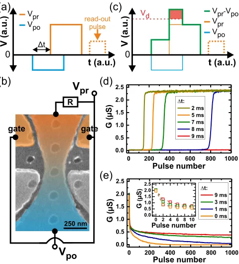
We also analyzed the conductance change in the mem-ristive operation mode when applying rectangular voltage pulses as shown in Fig. 4(a). These pulses mimic the input from a pre- and a post-synaptic neuron. The post-synaptic pulses with amplitude Vpo were applied to the QW and the pre-synaptic pulses with amplitude Vpr to the QW and the gates (see Fig. 4(b)). The pulses had a width of 10 ms and the time differenceDtwas varied. After each pulse, the con-ductance G was determined with a read-out pulse (dashed line). Fig. 4(c) depicts the voltage difference of the pulses. Discharging of the QD can occur during the red highlighted voltage range when the difference of both pulses exceeds the threshold voltage for discharging. The conductance versus the pulse number for amplitudesVpr¼3.8 andVpo¼ 0.8 V
FIG. 3. (a) Current-voltage characteristics of the memristive switching mode for temperatures of 4.2, 145, and 240 K. The pinched hysteresis loop is profound for 4.2 and 145 K, with its two clearly distinguishable conduc-tive states around zero bias. No pinched hysteresis loop is observed for T¼240 K. The curves are offset by 0.15lA. (b) Plateau width of the low conductive state versus temperature. The maximum operating temperature is found to be 165 K, as obtained from the exponential fit function after Eq. (4). No low conductive state is observed for higher temperatures. (c) Area of the hysteresis for positive and negative voltages versus temperature. The ex-ponential fit functions are based on Eq.(4).
FIG. 4. (a) Time trace of the pre- and post-synaptic voltage pulses which are applied to the source and the drain side, respectively. A read-out pulse with amplitude 1.2 V follows the pulses to determineG. (b) Circuit diagram when applying pre- and post-synaptic pulses to the two terminals of the memristor. (c) Difference of the post- and pre-synaptic pulses shown in (a) versus time. During the red shaded time interval, the voltage difference exceeds the threshold voltage for dischargingVd. (d) ConductanceGversus pulse num-ber. The pulses shown in (a) are applied to the memristor and the conduct-ance can be potentiated. Depending on Dt, the potentiation occurs after different pulse numbers. (e)Gversus pulse number for a depression of the conductance. For smallerDt, less pulses are needed to decreaseGto zero. The inset shows the conductance after the first pulses in more detail.
[image:4.612.54.294.52.229.2] [image:4.612.319.559.384.649.2]is presented in Fig.4(d). Initially, the QD was charged and the conductance was almost zero.Gremains unaltered when applying 1000 pulses with a time difference of 9 ms. LoweringDt to 8 ms results in an increase after 780 pulses and the conductance saturates at 2.4lS. This saturation is attributed to a completely discharged QD. Less pulses are needed to discharge the QD when the time difference is reduced. The amplitudes2.4 V and 0.8 V of the pre- and post-synaptic pulses, respectively, are used to decrease the conductance of an initially charged QD. The data are shown in Fig.4(e). For differentDt, the conductance is reduced by a large amount with only a few pulses. For smaller Dt, the change ofGis larger (see inset of Fig.4(e)). The decreasing conductance is attributed to a charging of the QD with elec-trons, which can be controlled with the time difference between the pre- and post-synaptic pulses.
In summary, we have presented a quantum dot floating gate transistor featuring a memristive operation mode. Sweeping closed voltage cycles allows to charge and dis-charge QDs in close vicinity of a 2DEG, resulting in a pinched hysteresis loop with two clearly distinguishable con-ductive states around zero bias. The memristive operation mode is observed up to temperatures of 165 K. The conduct-ance of the device can be controlled by the charging voltage or the time difference between rectangular voltage pulses applied directly to the source and drain contact. The pre-sented QD floating gate transistor with its memristive opera-tion mode may be considered to realize artificial synapses in future non-von Neumann computer architectures.
The authors gratefully acknowledge financial support from the European Union (FPVII (2007-2013) under Grant Agreement No. 318287 Landauer) as well as the state of Bavaria.
1
L. O. Chua,IEEE Trans. Circuit Theory18, 507–519 (1971). 2
L. O. Chua and S. M. Kang,Proc. IEEE64, 209–223 (1976).
3D. B. Strukov, G. S. Snider, D. R. Stewart, and S. R. Williams,Nature
453, 80–83 (2008). 4
A. Beck, J. G. Bednorz, Ch. Gerber, C. Rossel, and D. Widmer, Appl. Phys. Lett.77, 139–141 (2000).
5
K. Szot, W. Speier, G. Bihlmayer, and R. Waser,Nat. Mater.5, 312–320 (2006).
6A. Sawa, T. Fujii, M. Kawasaki, and Y. Tokura,Appl. Phys. Lett.88, 232112 (2006).
7
M. N. Kozicki, M. Park, and M. Mitkova,IEEE Trans. Nanotechnol.4, 331–338 (2005).
8
K. Terabe, T. Hasegawa, T. Nakayama, and M. Aono,Nature433, 47–50 (2005).
9Y. V. Pershin and M. Di Ventra,Phys. Rev. B78, 113309 (2008). 10M. Ziegler, M. Oberl€ander, D. Schroeder, W. H. Krautschneider, and H.
Kohlstedt,Appl. Phys. Lett.101, 263504 (2012). 11
C. Riggert, M. Ziegler, D. Schroeder, W. H. Krautschneider, and H. Kohlstedt,Semicond. Sci. Technol.29, 104011 (2014).
12
S. H. Jo, T. Chang, I. Ebong, B. B. Bhadviya, P. Mazumder, and W. Lu, Nano Lett.10, 1297–1301 (2010).
13B. Linares-Barranco and T. Serrano-Gotarredona, available from Nature Precedings, see hdl:10101/npre.2009.3010.1, 2009.
14
S. Song, K. D. Miller, and L. F. Abbott,Nat. Neurosci.3, 919–926 (2000). 15
G.-Q. Bi and M.-M. Poo, J. Neurosci.18, 10464–10472 (1998). 16R. C. Malenka and R. A. Nicoll,Science285, 1870–1874 (1999). 17
T. V. P. Bliss and G. L. Collingridge,Nature361, 31–39 (1993). 18
P. A. Merolla, J. V. Arthur, R. Alvarez-Icaza, A. S. Cassidy, J. Sawada, F. Akopyan, B. L. Jackson, N. Imam, C. Guo, Y. Nakamuraet al.,Science
345, 668–673 (2014).
19C. Schneider, A. Huggenberger, T. S€
unner, T. Heindel, M. Strauß, S. G€opfert, P. Weinmann, S. Reitzenstein, L. Worschech, M. Kamp, S. H€ofling, and A. Forchel,Nanotechnology20, 434012 (2009).
20P. Maier, F. Hartmann, M. Emmerling, C. Schneider, S. H€ ofling, M. Kamp, and L. Worschech,Appl. Phys. Lett.105, 053502 (2014). 21S. G€opfert, L. Worschech, S. Lingemann, C. Schneider, D. Press, S.
H€ofling, and A. Forchel,Appl. Phys. Lett.97, 222112 (2010). 22
L. Guo, E. Leobandung, and S. Y. Chou,Science275, 649–651 (1997). 23C. R. M€uller, L. Worschech, and A. Forchel,Phys. Rev. B 79, 205307
(2009). 24
S. P. Adhikari, M. P. Sah, H. Kim, and L. O. Chua,IEEE Trans. Circuits Syst. I60, 3008–3021 (2013).
25A. Schliemann, L. Worschech, S. Reitzenstein, S. Kaiser, and A. Forchel, Appl. Phys. Lett.81, 2115 (2002).
26
W.-H. Chang, T. M. Hsu, C. C. Huang, S. L. Hsu, C. Y. Lai, N. T. Yeh, T. E. Nee, and J.-I. Chyi,Phys. Rev. B62, 6959–6962 (2000).
27P. H€
anggi, P. Talkner, and M. Borkovec,Rev. Mod. Phys.62, 251–341 (1990).
203501-4 Maieret al. Appl. Phys. Lett.106, 203501 (2015)