Atomic-column scanning transmission electron microscopy analysis of misfit dislocations in GaSb/GaAs quantum dots
N. Fernández-Delgado*1, M. Herrera1, M. F. Chisholm2, M. A. Kamarudin3,4, Q.D. Zhuang3, M. Hayne3, S. I. Molina1
*Telephone number: +34 956 01 20 28; email: [email protected]
1 Department of Material Science, Metallurgical Engineering and Inorganic Chemistry, IMEYMAT, University of Cádiz, 11510, Puerto Real, Cádiz, Spain.
2 Scanning Transmission Electron Microscopy Group, Oak Ridge National Laboratory, Tennessee, USA.
3 Department of Physics, Lancaster University, Lancaster, LA1 4YB, UK
4 Department of Physics, Faculty of Science, Universiti Putra Malaysia, 43400 UPM Serdang, Selangor Darul Ehsan, Malaysia.
M. Herrera: [email protected]
M. F. Chisholm: [email protected]
M. A. Kamarudin: [email protected]
Q. D. Zhuang: [email protected]
M. Hayne: [email protected]
S. I. Molina: [email protected]
Abstract
The structural quality of GaSb/GaAs quantum dots (QDs) has been analyzed at atomic scale by aberration-corrected high-angle annular dark-field scanning transmission electron microscopy. In particular, we have studied the misfit dislocations that appear because of the high lattice mismatch in the heterostructure. Our results have shown the formation of Lomer dislocations at the interface between the GaSb QDs and the GaAs substrate, but also at the interface with the GaAs capping layer, which is not a frequent observation. The analysis of these dislocations point to the existence of chains of dislocation loops around the QDs. The dislocation core of the observed defects has been characterized, showing that they are reconstructed Lomer dislocations, which have less distortion at the dislocation core in comparison to unreconstructed ones. Strain measurements using geometric phase analysis (GPA) show that these dislocations may not fully relax the strain due to the lattice mismatch in the GaSb QDs.
Keywords
Electron microscopy, defects, crystal structure, epitaxial growth, thin films, dislocation loops
Introduction
is a promising semiconductor system with applications in devices such as lasers[1] or photodetectors [2]. Type-II GaSb/GaAs quantum dots (QDs) can extend the spectral response beyond the visible towards 1.4 µm providing a near optimum band gap for concentrator solar cell applications [3]. However, the epitaxial growth of this material has the drawback of high lattice mismatch (7.8%) between the active layer, GaSb, and the substrate, GaAs, which causes the formation of structural defects such as dislocations[4,5]. These defects are detrimental to the optoelectronic properties of the material because additional electronic states within the band gap lead to nonradiative recombination that affect the electronic and optical properties[6,7].
Different alternatives have been proposed in the growth of semiconductor materials with high lattice mismatch to avoid structural defects, such as the growth of strained superlattice layers [8] or thermal annealing [9]. Special attention is given to the interfacial misfit dislocation (IMF) method [10,7], which has the objective of favoring Lomer dislocations in high-lattice-mismatch systems to provide plastic relaxation without the appearance of threading dislocations. In order to improve the structural quality of these epitaxial nanostructures, a better understanding of the formation and characteristics of these misfit dislocations is required.
In this work, we analyze GaSb/GaAs nanostructures by atomic-column resolution high-angle annular dark-field scanning transmission electron microscopy (HAADF-STEM), where the formation of a double Lomer dislocation network likely due to the presence of dislocation loops around the QDs has been found. The strain relaxation of the high lattice mismatch GaSb/GaAs QDs produced by these dislocations is measured and analyzed.
Materials and methods
The sample studied consists of nanostructures of GaSb grown on a GaAs (001) substrate by molecular beam epitaxy. Initially, a GaAs buffer layer with a thickness of 250-350 nm was grown at 580ºC at a growth rate of 1 MLs-1. Subsequently, the substrate temperature was reduced to 490ºC for the deposition of the GaSb with a deposition rate of 0.3 MLs-1 for 7 s, reaching a thickness of 2.1 ML. After that, the structure was capped with ̴10 nm of GaAs at 430ºC with a growth rate of 1 MLs-1. A conventional method was used for transmission electron microscopy specimen preparation, consisting of mechanical thinning using SiC paper and Ar+ ion milling using a precision ion polishing system. The sample was studied by HAADF-STEM using a NION UltraSTEM 200 aberration corrected microscope working at 200 kV. Geometric phase analysis (GPA) [11] was used to investigate the local strain distribution. This method provides quantitative information about local atomic shifts in the region of interest obtained by comparison with an unstrained reference zone, in our case the GaAs substrate.
Results
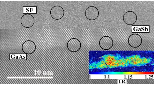
the image in Fig. 1 and calculated using the qHAADF algorithm [12] is included as an inset. The methodology used to build this map consists of detecting the intensity maxima in the image and then measuring intensities integrated in a certain area at the regions of interest with regards to the maxima found. The intensity ratio (I. R.) corresponding to that in the region of interest divided by the intensity in a region taken as a reference, (in this particular case, the GaAs substrate) leads to the intensity map. As can be observed, the GaSb QD in Fig. 1 has an elongated shape. The dimensions of the QDs in this sample has been measured from the intensity maps, obtaining average diameters of 20±3 nm and heights of 6.7±1.3 nm. The QD in Fig. 1 contains a planar defect, which has been characterized as an intrinsic stacking fault (SF). This type of defect is not frequent in the sample. A closer look at the HAADF-STEM image in Fig. 1 shows the presence of dislocations at the GaSb/GaAs interface, marked with circles. However, it should be highlighted that dislocations have also been observed at the interface of the QDs with the GaAs capping layer, which is something significant. Frequently, misfit dislocations (MDs) are created at the interface of heteroepitaxial layers with the substrate when the critical thickness is exceeded. This has been commonly observed in a wide range of systems like InGaAs/GaAs [13], GaSb/GaAs [14] or ZnTe/GaAs [15], and in active layers with different morphologies including 2D layers [16] and 3D [17,18] nanostructures. However, the observation of MDs at the interface with the capping layer is less common. As shown for in InAs/GaSb 2D systems, the strain may be different at both interfaces[19]. With the aim of obtaining additional information, the analysis of the observed dislocations has been carried out.
Fig. 1 HAADF-STEM image of GaSb QDs in the sample, where its intensity map has been included as an inset. Dislocations are observed in the image at both interfaces of the QD, with the substrate and with the capping layer.
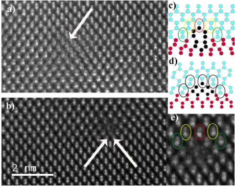
that the observed dislocation can be identified as a reconstructed Lomer dislocation. All the Lomer dislocations observed in the studied sample have been characterized as reconstructed Lomer dislocations. This type of dislocation core causes less distortion of the surrounding matrix than the unreconstructed ones [7], being a more stable configuration.
Fig. 2 HAADF-STEM images of a 60º dislocation (a) and a Lomer dislocation (b) found in the sample, where the extra half-planes have been marked with arrows. Schematic of reconstructed (c) and unreconstructed (d) Lomer dislocations cores. e) Detail of a dislocation core that is consistent with a reconstructed Lomer dislocation; different colours have been used to aid comparison of the atoms in the scheme and the STEM image.
also been found, which are less efficient in strain relaxation. In order to obtain a more accurate value of the relaxation degree in the analyzed QDs and to obtain more detailed information on the strain in the heterostructure, GPA has been applied to the obtained HAADF-STEM images.
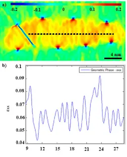
GPA has been widely used to study the strain in different semiconductors [27,28] including GaSb/Si 2D layers [29] or GaSb/GaAs 2D layers[30]. Fig. 3 shows the strain map εxx (in the direction contained in the growth plane) of the QD in Fig. 1. Lomer dislocations appear as blue and red lobular shapes corresponding to the strain distribution around the dislocation; the blue lobes show compressive strain fields, and the red tensile strains. The strain map shows that the dislocations at the upper interface have opposite Burger vectors to those at the bottom interface, as expected. This is deduced from the inversion in the position of the blue-red lobes associated to the dislocations. With regard to the QD, it can be seen that the strain in this nanostructure is above zero. It should be mentioned that this strain is measured with regard to the lattice parameter of the GaAs substrate and not to a relaxed GaSb material. Because of this, a fully relaxed GaSb layer would show a strain value equal to the lattice mismatch between the active layer and the substrate, as observed in GaSb/Si [29]. In this case, the lattice mismatch of the GaSb layer with the GaAs substrate is 7.8%. A strain profile has been taken along the dotted line included in the strain map of Fig. 3 a), and it is shown in Fig. 3 b). This strain profile shows that the average value of strain in the QD is 6.4±1.2%. The strain variability inside the QDs is similar to that found in the substrate and, in consequence, is not significant.
Fig. 3 a) Strain map obtained from the HAADF-STEM image in Fig. 1 using the GPA. b) Strain linescan obtained from the dotted line in the map in a).
Discussion
Lomer dislocations have been widely reported at the GaSb/GaAs interface both in 2D layers [33,20] and in 3D QDs [21,17]. These dislocations are more effective for the plastic relaxation of epitaxial systems than classical 60º ones. Also, they are advantageous for the functional properties of semiconductor heterostructures because they do not have threading segments crossing the different layers of the system. Because of this, attention has been paid to the optimization of the growth conditions in high lattice mismatch systems such as GaSb/GaAs in order to obtain Lomer dislocation networks, in what is called the IMF method [4,21]. In this sense, it has been observed that a high lattice mismatch between the active layer and the substrate [34] or the high growth temperature [33,35] benefit the IMF growth method. The IMF method is very effective for the reduction of the threading dislocation density in highly mismatched systems[33], and it is able to produce an almost full relaxation of the lattice mismatch in 2D layers [33].
[image:6.595.171.428.69.385.2]vectors, as obtained in our GPA analysis. However, epitaxial growth is a non-equilibrium process, where parameters such as the growth temperature or the flux conditions play an important role in defect formation [35,33], producing deviations from the theoretical predictions. On the other hand, in 3D nanostructures the dislocations configuration is expected to be different than in 2D layers. In 2D epitaxial layers misfit dislocations can glide along the large interface with the substrate forming long dislocation lines. However, this interface is limited in QD, therefore these dislocations could have a different configuration.
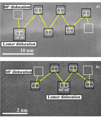
In the literature, two publications have reported dislocations at both interfaces of 3D nanostructures, in InSb/GaSb QDs [37] and in InN/GaN QDs [38]. In both cases, the dislocations have been characterized as 60º. In ref. [37] the authors interpret their finding as the existence of dislocation loops around the QDs that allows their plastic relaxation. In our study, the absence of threading dislocations also suggests that the dislocations observed here form dislocation loops around the QDs. The observed Lomer dislocations can be decomposed into two 60º dislocations. These 60º dislocations in a QDs can be grouped in pairs, in such a way that the dislocations in a pair are located at different interfaces but lying on the family of {111} planes and having opposite Burgers vectors. This is consistent with each of these dislocation pairs corresponding to a dislocation loop. Fig. 4 a) shows the HAADF image of the QD analyzed in Figs 1 and 3, where all the 60º dislocations are marked with white squares, and dislocation pairs forming possible dislocations loops are linked with yellow lines. It seems that the relaxation of these QDs occurs through the formation of a chain of dislocation loops, with a different number depending on the QD size. This is also consistent with the observation that there are always two 60º dislocations, which are found at the outermost edge of an array. Two different configurations of these 60º dislocations have been observed, depending on the number of dislocation loops in a QD: one at the opposite end of each dislocation array (one at the upper interface and the other at the lower interface), as shown is Fig. 4 a), and at the opposite ends of the same dislocations array, as shown in Fig. 4 b).
Fig. 4 HAADF images of GaSb/GaAs QDs, where possible dislocation loops are marked with yellow lines, showing the configuration of 7 (a) and 6 (b) dislocation loops. 60º dislocations are marked with white squares and Lomer dislocations with black squares.
Conclusion
The analysis by HAADF of GaSb/GaAs QDs has shown the presence of Lomer dislocations at the interface of the QDs with the substrate, but also at the interface with the GaAs capping layer, which has not frequently been reported. The analysis of these dislocations indicates the existence of chains of dislocation loops around the QDs. The cores of the dislocations have been characterized from high-resolution HAADF images, showing that they are reconstructed dislocations. The analysis of the strain in the heterostructure using the GPA method has shown that the observed dislocation network may not produce a full relaxation of the lattice mismatch in the GaSb QDs.
Acknowledgements
This work was supported by the Spanish MINECO (projects TEC2014-53727-C2-2-R and CONSOLIDER INGENIO 2010 CSD2009-00013), and Junta de Andalucía (PAI research group TEP-946). The research leading to these results has received funding from the European Union H2020 Program (PROMIS ITN European network). STEM observations, carried out at Oak Ridge National Laboratory, were sponsored by the U.S. DOE Office of Science, Basic Energy Sciences, Materials Sciences and Engineering Division.
Conflict of interest
The authors declare that no conflicts of interest exists, that could potentially influence or bias the submitted work.
[image:8.595.194.402.69.311.2]1. Munnelly P, Heindel T, Karow MM, Höfling S, Kamp M, Schneider C, Reitzenstein S (2015) A pulsed nonclassical light source driven by an integrated electrically triggered quantum dot microlaser. IEEE Journal on Selected Topics in Quantum Electronics 21 (6):1900609-9. doi:10.1109/JSTQE.2015.2418219
2. Downs C, Vandervelde TE (2013) Progress in infrared photodetectors since 2000. Sensors (Switzerland) 13 (4):5054-5098. doi:10.3390/s130405054
3. Carrington PJ, Mahajumi AS, Wagener MC, Botha JR, Zhuang Q, Krier A (2012) Type II GaSb/GaAs quantum dot/ring stacks with extended photoresponse for efficient solar cells. Physica B: Condensed Matter 407 (10):1493-1496. doi:10.1016/j.physb.2011.09.069
4. Laghumavarapu RB, Moscho A, Khoshakhlagh A, El-Emawy M, Lester LF, Huffaker DL (2007) GaSbGaAs type II quantum dot solar cells for enhanced infrared spectral response. Applied Physics Letters 90 (17):173125-3. doi:10.1063/1.2734492 5. Smakman EP, Garleff JK, Young RJ, Hayne M, Rambabu P, Koenraad PM (2012) GaSb/GaAs quantum dot formation and demolition studied with cross-sectional scanning tunneling microscopy. Applied Physics Letters 100 (14):142116-3. doi:10.1063/1.3701614
6. Schaller RD, Klimov VI (2004) High efficiency carrier multiplication in PbSe nanocrystals: Implications for solar energy conversion. Physical Review Letters 92 (18):186601-3. doi:10.1103/PhysRevLett.92.186601
7. Lopatin S, Duscher G, Pennycook SJ, Chisholm MF (2002) Z-contrast imaging and EELS of dislocation cores at the Si/GaAs interface. Applied Physics Letters 81 (15):2728-2730. doi: 10.1063/1.1511808
8. Haugan HJ, Brown GJ, Elhamri S, Grazulis L (2015) Control of anion incorporation in the molecular beam epitaxy of ternary antimonide superlattices for very long wavelength infrared detection. Journal of Crystal Growth 425:25-28. doi:http://dx.doi.org/10.1016/j.jcrysgro.2015.03.008
9. Wang W, Gan X, Xu Y, Wang T, Wu H, Liu C (2015) High-quality n-type aluminum gallium nitride thin films grown by interrupted deposition and in-situ thermal annealing. Materials Science in Semiconductor Processing 30:612-617. doi:http://dx.doi.org/10.1016/j.mssp.2014.11.010
10. Balakrishnan G, Tatebayashi J, Khoshakhlagh A, Huang SH, Jallipalli A, Dawson LR, Huffaker DL (2006) III/V ratio based selectivity between strained Stranski-Krastanov and strain-free GaSb quantum dots on GaAs. Applied Physics Letters 89 (16):161104-3. doi:10.1063/1.2362999
11. Hÿtch MJ, Snoeck E, Kilaas R (1998) Quantitative measurement of displacement and strain fields from HREM micrographs. Ultramicroscopy 74 (3):131-146. doi:10.1016/S0304-3991(98)00035-7
12. Molina SI, Sales DL, Galindo PL, Fuster D, González Y, Alén B, González L, Varela M, Pennycook SJ (2008) Column-by-column compositional mapping by Z-contrast imaging. Ultramicroscopy 109:172-176. doi:10.1016/j.ultramic.2008.10.008 13. Rudinsky ME, Karpov SY, Lipsanen H, Romanov AE (2015) Critical thickness and bow of pseudomorphic InxGa1-xAs-based laser heterostructures grown on (001)GaAs and (001)InP substrates. Materials Physics and Mechanics 24 (3):278-283. doi:10.1134/S1063782613090054
15. Kim TW, Lee DU, Lee HS, Lee JY, Park HL (2001) Strain effects and atomic arrangements of 60° and 90° dislocations near the ZnTe/GaAs heterointerface. Applied Physics Letters 78 (10):1409-1411. doi:10.1063/1.1349866
16. Noh YK, Hwang YJ, Kim MD, Kwon YJ, Oh JE, Kim YH, Lee JY (2007) Strucrural properties of GaSb layers grown on InAs, AlSb, and GaSb buffer layers on GaAs (001) substrates. Journal of the Korean Physical Society 50 (6):1929-1932. doi:10.3938/jkps.50.1929
17. Kim YH, Lee JY, Noh YG, Kim MD, Oh JE (2007) High-resolution transmission electron microscopy study on the growth modes of GaSb islands grown on a semi-insulating GaAs (001) substrate. Applied Physics Letters 90 (24):241915-3. doi:10.1063/1.2747674
18. Fazouan N, Atmani E, El Kasri F, Rouhani MD, Esteve A (2011) Interface structure of deposited GaSb on GaAs (001): Monte Carlo simulation and experimental study. Journal of Materials Science 47 (4):1684-1689. doi:10.1007/s10853-011-6018-2
19. Mahalingam K, Haugan HJ, Brown GJ, Eyink KG (2013) Quantitative analysis of interfacial strain in InAs/GaSb superlattices by aberration-corrected HRTEM and
HAADF-STEM. Ultramicroscopy 127:70-75.
doi:http://dx.doi.org/10.1016/j.ultramic.2012.09.005
20. Wang Y, Ruterana P, Chen J, Kret S, El Kazzi S, Genevois C, Desplanque L, Wallart X (2013) Antimony-mediated control of misfit dislocations and strain at the highly lattice mismatched GaSb/GaAs interface. ACS Applied Materials and Interfaces 5 (19):9760-9764. doi:10.1021/am4028907
21. Huang SH, Balakrishnan G, Khoshakhlagh A, Jallipalli A, Dawson LR, Huffaker DL (2006) Strain relief by periodic misfit arrays for low defect density GaSb on GaAs. Applied Physics Letters 88 (13):131911-3. doi:10.1063/1.2172742
22. Jallipalli A, Balakrishnan G, Huang SH, Khoshakhlagh A, Dawson LR, Huffaker DL (2007) Atomistic modeling of strain distribution in self-assembled interfacial misfit dislocation (IMF) arrays in highly mismatched III-V semiconductor materials. Journal of Crystal Growth 303 (2):449-455. doi:10.1016/j.jcrysgro.2006.12.032
23. Silveira JP, Briones F (1999) In situ observation of reconstruction related surface stress during molecular beam epitaxy (MBE) growth of III–V compounds. Journal of Crystal Growth 201–202 (0):113-117. doi:http://dx.doi.org/10.1016/S0022-0248(98)01301-3
24. Suzuki K, Hogg RA, Arakawa Y (1999) Structural and optical properties of type II GaSb/GaAs self-assembled quantum dots grown by molecular beam epitaxy. Journal of Applied Physics 85 (12):8349-8352. doi:http://dx.doi.org/10.1063/1.370622
25. Matthews JW, Blakeslee AE (1974) Defects in epitaxial multilayers: I. Misfit dislocations. Journal of Crystal Growth 27 (0):118-125. doi:http://dx.doi.org/10.1016/S0022-0248(74)80055-2
26. Fu K, Fu Y (2009) Strain-induced Stranski-Krastanov three-dimensional growth mode of GaSb quantum dot on GaAs substrate. Applied Physics Letters 94 (18):181913-3. doi:10.1063/1.3132054
27. He XQ, Wen C, Duan XF, Chen H (2011) Identification of atomic steps at AlSb/GaAs hetero-epitaxial interface using geometric phase method by high-resolution electron microscopy. Materials Letters 65 (3):456-459. doi:10.1016/j.matlet.2010.10.054
29. Vajargah SH, Couillard M, Cui K, Tavakoli SG, Robinson B, Kleiman RN, Preston JS, Botton GA (2011) Strain relief and AlSb buffer layer morphology in GaSb heteroepitaxial films grown on Si as revealed by high-angle annular dark-field scanning transmission electron microscopy. Applied Physics Letters 98 (8):082113-3. doi:10.1063/1.3551626
30. Zhou W, Tang W, Lau KM (2011) A strain relief mode at interface of GaSb/GaAs grown by metalorganic chemical vapor deposition. Applied Physics Letters 99 (22):221917-3. doi:doi:http://dx.doi.org/10.1063/1.3663571
31. Hernández-Saz J, Herrera M, Molina SI, Stanley CR, Duguay S (2015) 3D compositional analysis at atomic scale of InAlGaAs capped InAs/GaAs QDs. Scripta Materialia 103:73-76. doi:10.1016/j.scriptamat.2015.03.013
32. Li L, Liu G-j, Wang Y, Li M (2005) GaSb film growth on GaAs substrate by MBE. In: Source of the DocumentProceedings of SPIE - The International Society for Optical Engineering: 602038. doi: 10.1117/12.635146
33. Huang S, Balakrishnan G, Huffaker DL (2009) Interfacial misfit array formation for GaSb growth on GaAs. Journal of Applied Physics 105 (10):103104-5. doi:10.1063/1.3129562
34. Mallard RE, Wilshaw PR, Mason NJ, Walker PJ, Booker GR (1989) Lattice-Relaxation Of Strained GaSb GaAs Epitaxial Layers Grown By MOCVD. Institute Of Physics Conference Series:331-336. doi:http://ora.ox.ac.uk/objects/uuid:a73bbcb1-5119-4fbf-93c8-6ca6ecf1e733
35. Kim JH, Seong TY, Mason NJ, Walker PJ (1998) Morphology and defect structures of GaSb islands on GaAs grown by metalorganic vapor phase epitaxy. Journal of Electronic Materials 27 (5):466-471. doi:10.1007/s11664-998-0178-0
36. Matthews JW, Blakeslee AE (1974) Defects in epitaxial multilayers. I. Misfit dislocations. Journal of Crystal Growth 27 (C):118-125. doi:http://dx.doi.org/10.1016/S0022-0248(74)80055-2