University of Warwick institutional repository: http://go.warwick.ac.uk/wrap
This paper is made available online in accordance with publisher policies. Please scroll down to view the document itself. Please refer to the repository record for this item and our policy information available from the repository home page for further information.
To see the final version of this paper please visit the publisher’s website. Access to the published version may require a subscription.
Author(s): James D. Aldous, Christopher W. Burrows, Ana M.
Sánchez, Richard Beanland, Ian Maskery, Matthew K. Bradley, Manuel dos Santos Dias, Julie B. Staunton, and Gavin R. Bell
Article Title: Cubic MnSb: Epitaxial growth of a predicted room temperature half-metal
Year of publication: 2012 Link to published article:
LG13382
REVIEW COPY
NOT FOR DISTRIBUTION
Cubic MnSb: epitaxial growth of a predicted room temperature
half-metal
James D. Aldous, Christopher W. Burrows, Ana M. S´anchez,
Richard Beanland, Ian Maskery, Matthew K. Bradley, Manuel
dos Santos Dias, Julie B. Staunton, and Gavin R. Bell∗
Department of Physics, University of Warwick, Coventry, UK, CV4 7AL
(Dated: January 26, 2012)
Abstract
Epitaxial films including bulk-like cubic and wurtzite polymorphs of MnSb have been grown by
molecular beam epitaxy on GaAs via careful control of the Sb4/Mn flux ratio. Nonzero-temperature
density functional theory was used to predictab initio the half metallicity of the cubic polymorph and compare its spin polarization as a function of reduced magnetization with that of the well
known half-metal NiMnSb. In both cases, half-metallicity is lost at a threshold magnetization
reduction, corresponding to a temperatureT∗ < TC. This threshold is far higher for cubic MnSb
compared to NiMnSb and corresponds to T∗ > 350K, making epitaxial cubic MnSb a promising
candidate for efficient room temperature spin injection into semiconductors.
A key goal for the development of semiconductor (SC) spintronics is efficient electrical
injection of spin polarized current into a non-magnetic SC structure. Ferromagnetic (FM)
materials can be used as a spin source and an ideal material would both provide a fully
spin polarized current1,2 and possess “engineering compatibility” with its SC host. This
includes controllable epitaxy and interfaces, and suitability for device processing. Certain
half-metallic ferromagnetic (HMF) materials have a theoretical density-of-states (DOS) spin
polarization at the Fermi level of PDOS = 100% due to the presence of a band gap
strad-dling the Fermi energy EF for one spin channel only3. Density functional theory (DFT)
has predicted this property in several classes of materials1–3
, including Heusler alloys and
transition metal pnictides (TMPs), at temperature T = 0K. On this basis, half-metallicity
was first envisaged in the ternary Heusler alloy NiMnSb, which has a minority spin gap
Eg ≈0.5 eV4. However, there is presently no HMF candidate with SC engineering
compati-bility which clearly maintainsPDOS ≈100% at room temperature. DFT studies continue to
play a key role both in assessing the potential of new HMF materials and in understanding
fundamental aspects of the HMF state.
Experimental verification ofPDOSis not straightforward and after more than two decades’
study,PDOS(T) for NiMnSb is not known. For example, spin polarized photoemission
spec-troscopy (SPPES) can measure PDOS quite directly, but it is strongly affected by
extrin-sic effects (e.g. non-stoichiometry, reduced magnetization, reconstruction) at the surface.
Threshold SPPES measured PDOS ≤ 50% atT = 20K5, while more recent works measured
40%6
, or 50% at T = 10K7
. Note that spin polarizations in electron transport are not the
same as PDOS, and have been inferred from magnetic tunnel junctions (MTJs) or spin light
emitting diodes8, or by Andreev reflection9. Useful magnetoresistance has been achieved in
MTJs with Heusler alloy contacts1. While extrinsic effects can alter spin polarization, such
problems can be tackled by improving material quality10 and epitaxy11. It remains crucial
to address what are the intrinsic limitations onPDOS.
HMF band structures are expected to change as T increases, even well below the Curie
temperatureTC2,12–14. Theory shows how the DOS in the minority spin gap becomes nonzero
as a consequence of the effects of thermally induced spin fluctuations on the electronic
structure. In fact, beyond a threshold temperature T∗ < T
C, the value of PDOS collapses
far more rapidly than the reduction of magnetization M(T)12. This effect may set an
spintronics. An HMF material with a larger Eg, as we show later in this letter, can be
expected to have a much higher T∗.
The binary TMPs have attracted much recent attention. Materials such as MnAs and
CrSb are predicted to be HMF with large Eg in cubic (sphalerite)15,16 and wurtzite17 (w-)
polymorphs. Here, we predict cubic c-MnSb to be HMF withEg = 1.08 eV, unlike naturally
occurring B81 niccolite structure n-MnSb which is a normal FM metal. Attempts have
been made to stabilize cubic TMP polymorphs by high-strain epitaxial growth on common
SC substrates, e.g. c-CrAs and c-CrSb grown as ultra-thin films on GaAs(001). However,
these films revert to their stable non-HMF structures within 2-4 nm thickness15,18 while
X-ray diffraction (XRD) has shown the presence of strained orthorhombic o-CrAs rather
than c-CrAs19. A recent DFT study of CrAs on GaAs(001) found that bulk-like o-CrAs was
favorable for ultra-thin films with just 3 Cr atomic layers, and argued that reported FM
hysteresis is due to uncompensated interfacial spins of anti-FM o-CrAs20. Highly strained
epitaxy does not appear to be a promising route to producing wide-gap HMF thin films of
this class and we demonstrate an alternative route in this letter.
We report here the first fully ab initio DFT calculations which compare the nonzero-T
electronic structure and spin polarization of binary c-MnSb and ternary NiMnSb. These
demonstrate that c-MnSb, with its large value of Eg, possesses far more robust
half-metallicity than the Heusler alloy. Furthermore, we show for the first time that c-MnSb
and w-MnSb can be grown epitaxially on GaAs by careful flux control in molecular beam
epitaxy (MBE) without relying on heteroepitaxial strain to stabilize the polymorphs.
We first calculated the T = 0 electronic properties of n-, c- and w-MnSb polymorphs
using two standard DFT packages21,22. (Full details will be given in a longer paper.) Both
c-MnSb and w-MnSb are HMF materials with Eg 1.08 eV and 1.15 eV respectively and
integer total spin moment 4µB at T = 0K. The calculated electronic structure of n-MnSb
agrees with previous work23and shows a weak P
DOS of 18%. The change of MnSb structure
from n- to c- or w-phases represents true polymorphism since there is a change of bonding
from octahedral coordination of Mn by surrounding Sb to tetrahedral coordination of both
elements. Conversely, the c- and w- phases are mutual polytypes, differing only in the
stacking sequence of (111) or (0001) planes. As expected, they are very close in total energy,
calculated respectively at 0.829 and 0.833 eV per formula unit above n-MnSb.
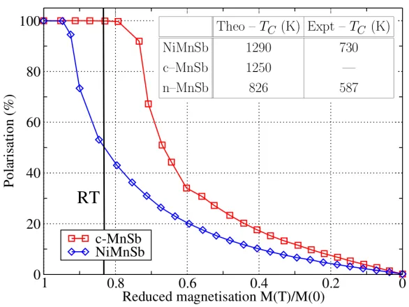
RT
FIG. 1. (color online) Nonzero-T electronic structure theory for MnSb and NiMnSb. The curves show the calculated Fermi level spin polarizationPDOSas a function of magnetization reduction for
c-MnSb (red squares) and NiMnSb (blue diamonds), while the inset table summarizes calculated
TC values from DLM-DFT. The experimental lattice parameter was assumed for c-MnSb, and the
value used for NiMnSb matched that of Ref.12. The vertical line labelled RT represents room
temperature, assuming the experimental TC of NiMnSb for both materials.
to estimate T∗ we have extended the modelling of the c-MnSb and n-MnSb polymorphs to
nonzero-temperature DFT using the disordered local moment (DLM) theory24,25. The
the-ory includes the effects of thermally induced spin fluctuations on the underlying electronic
structure, which must destroy the long-range magnetic order and the overall spin
polariza-tion of the electronic states at T ≥ TC. The DLM-DFT approach associates a local spin
polarization axis ˆei or local moment with each lattice site, i. These axes vary slowly on the
timescale of the electronic motions, affecting the nature and extent of the spin polarization of
the electronic structure and being self-consistently maintained. Thermally-induced disorder
in the orientations of the local moments is treated using a mean-field scheme, based on the
coherent potential approximation26,27. A generalisation of DFT is used to give an energy for
a given orientational configuration of the local moments,{eˆi},i.e. Ω{eˆi}. By taking ensemble
averages over the local moments’ orientational configurations with each configuration given a
[image:5.612.156.449.74.294.2]-4
-3
-2
-1
0
1
2
Energy from Fermi level (eV)
-9
-6
-3
0
3
6
9
DOS (states/eV)
M(T)/M(0) = 1.00
M(T)/M(0) = 0.79
M(T)/M(0) = 0.00
FIG. 2. (color online) Spin-polarized DOS for c-MnSb at different magnetizationsM(T) calculated
by DLM-DFT at the experimental lattice parameter. The three curves correspond toT = 0K (blue
dash),T =T∗ (red dash-dot) andT =TC (black solid line): the upper panel shows majority spin
DOS, the lower minority spin DOS.
able to determine the system’s magnetic properties. These are underpinned by spin
polar-ized electronic structure which varies according to the extent of magnetic order, M(T). We
can therefore findPDOS versus (M(T)/M(0)). DLM-DFT theory also describesab initio the
onset and type of magnetic order24,25 with an estimate of magnetic transition temperatures.
Details can be found in refs.28,29.
Results of our DLM-DFT calculations are summarized in Fig. 1. The inset tabulates the
Curie temperatures for n-MnSb and NiMnSb: in each case our calculated TC is larger than
the experimental value as expected from mean field estimates. Other similar calculations12
for NiMnSb have also somewhat overestimatedTC. In accord with experiment, however, the
theory estimates theTC of NiMnSb to be significantly higher than that of n-MnSb. Our
cal-culated TC values for NiMnSb and c-MnSb are very similar. That TC ≫ 300 K for c-MnSb
is promising but, noted above, does not guarantee a high PDOS at room temperature14.
The behavior of PDOS predicted by DLM-DFT as a function of magnetization reduction,
[image:6.612.130.481.70.329.2]hor-izontal axis is effectively a distorted temperature scale between 0 and TC. For NiMnSb,
PDOS rapidly collapses after just a 5% reduction in magnetization. The same behavior is
evident for c-MnSb but in this case PDOS remains at 100% to a much higher magnetization
reduction of around 21%. Using DLM-DFT to estimate the magnetization dependence on
temperature M(T) we can compare T∗ of NiMnSb and c-MnSb. We find that T∗ ≈ 0.14T
C
for NiMnSb which translates to 100K or 180K depending on whether the experimental or
theoretical value of TC is used. For c-MnSb T∗ ≈ 0.48 TC, i.e. T∗ ≈ 350 K or 620 K using
theTC values of NiMnSb and we deduce that the half-metallicity of c-MnSb is robust against
thermal spin fluctuations even above room temperature.
This property stems from the large Eg. In c-MnSb the nearest neighbours of each Mn
atom are 4 Sb atoms. The local tetrahedral environment enables the t2g states of Mn to
hybridize easily with the Sb p-states so that a large bonding-antibonding splitting is set up
where the lower-lying bonding states have more p-character whilst the higher antibonding
states are more d-like. The gap in between is partly filled by the non-bonding narrow eg
states of the transition metal. At T = 0K Mn has a large exchange splitting which causes
the bands of the majority and minority spin electrons to be distributed around different
energies30, E
maj, Emin. The majority spin d-states of the Mn atoms are closer to the Sb
p-states and the bonding-antibonding gap is smaller. For the minority spin electrons the
Mn d-states are forced higher by the exchange splitting and the gap for this spin channel
straddles EF with the anti-bonding states unfilled.
At a given T andM(T) the overall spin polarization of the electronic structure is given by
the average over an ensemble of non-collinear local moment configurations, {eˆi}, weighted
by P{eˆi}24. When M(T)/M(0) is slightly less than unity there is a small chance of a
spin-polarized electron encountering a local moment not aligned with the overall magnetization
direction. This leads to a small “impurity” majority spin DOS close to Emin and a small
“impurity” minority spin DOS near Emaj. As M(T)/M(0) diminishes these features grow
so that a signature of the exchange splitting of the electronic structure persists even above
TC which sustains the local moments despite their orientations becoming disordered. These
features are illustrated for c-MnSb in Fig. 2. The minority spin gap Eg = 1.08 eV appears
in the fully magnetized case corresponding to T = 0K (blue curve). The exchange splitting
between the antibonding t2g states of the majority and minority spin channels is large so
electrons appear in the majority spin channel aboveEF whilst majority spin impurity states
form in the minority spin gap close to the position of the antibonding t2g majority spin
band. As M is reduced, these encroach up to the Fermi level and at T∗ remove the
half-metallicity abruptly. If Eg were smaller this disruption would happen at a lower T∗. This
mechanism is shown in the red curve of Fig. 2: the impurity states have just reached EF at
a magnetization reduction of 21%, initiating the collapse of PDOS shown in Fig. 1. Finally,
for T > TC all spin polarization is lost (black curve). The same effects occur for NiMnSb
but at a much lower T∗.
The changes to the DOS which occur as T is increased reflect the effect of spin wave
dis-order on the quasi-particle excitations. Indeed our DLM treatment of essentially transverse
magnetic fluctuations can be considered as the static limit of some, as yet undeveloped,
dynamical mean field theory of spin fluctuations31. There have also been a number of
theoretical studies by Katsnelson, Chioncel and co-workers33 of electron correlation effects
beyond what is available from conventional DFT on the electronic structure of putative
HMFs. They set up a multi-orbital Hubbard-type model selecting reasonable U and J
pa-rameters. Their subsequent many- body theory analysis focusses on specific effects and
shows how dynamical electron-electron correlations may introduce non-quasiparticle states
into the minority spin gap. These new minority spin DOS features are qualitatively different
from those found for the DLM-DFT shown in Fig. 2. It would be interesting to see this
analysis carried out for the T-dependence of spin-polarized DOS of c-MnSb, compared with
that NiMnSb together with estimates of theTc’s and to find out whether the half-metallicity
of c-MnSb is also robust to increase in T within this approach.
These conclusions add strong impetus to the search for cubic TMP thin films stabilized
on SC substrates20. We have performed MBE growth of MnSb on GaAs and succeeded in
stabilizing cubic and wurtzite polymorphs in films tens of nm thick without high
epitax-ial strain. The MnSb films were grown on ∼10 mm wide GaAs(111) substrates by MBE,
without substrate rotation34. The substrate temperature T
sub was fixed at 695±5 K, and
the growth rate was 6 nm min−1. For each growth run the Sb
4/Mn flux ratio J was
mea-sured directly by a retractable ionization gauge. Typically, samples were capped with Sb to
prevent oxidation35. Specimens were prepared for transmission electron microscopy (TEM)
using conventional techniques. They were examined using JEOL 2000FX and Tecnai F20
FIG. 3. (color online) TEM data for polymorphic MnSb films on GaAs(111). A typical bright-field
image (a) and Fourier transforms from individual regions (b) are labelled with constituent phases,
while a high resolution micrograph of the c-MnSb/n-MnSb boundary shows a sharp epitaxial
interface.
area diffraction patterns (SADP).
In Fig. 3 we show TEM data from typical polymorphic films. Initially the epilayer
grows as n-MnSb, with a high density of misfit dislocations at the n-MnSb/GaAs interface
efficiently relaxing the 3.2% in-plane strain within a few nm thickness34. However, beyond
a certain film thickness (typically 100 nm) a sharp transition to polymorph growth occurs.
Careful analysis of the images and SADP reveals that two epitaxial polymorphs of MnSb
exist in the upper portion of the films, namely c-MnSb(111) and w-MnSb(0001). Calibrating
SADP data to the GaAs substrate gives the following lattice parameters (in ˚A, uncertainty
±0.5%): n-MnSb a=4.115, c=5.769; w-MnSb a=4.291, c=7.003; c-MnSb a=6.502. For
n-MnSb, the lattice parameters conform with results in the literature23,34
, which gives us
confidence in the w-MnSb and c-MnSb values, while for w-MnSb, the c/a ratio is almost
exactly 1.632 =p
8/3, corresponding to tetrahedral coordination of nearest neighbours. The
experimental lattice parameters match the trends from optimized DFT structures. For the
[image:9.612.189.422.71.333.2]translational domains a single epitaxial orientation is predicted36. The interface between
n-MnSb and the polymorph epilayer is sharp, as shown by the high resolution image in Fig. 3,
and maintains the epitaxial relationship. We see no TEM evidence for translational domains
and associated double positioning boundaries in the epilayer due to pre-existing GaAs surface
steps. The polymorph growth is not influenced by post-growth cycling between 300 K and
700 K and the film structure is stable for many months, provided the samples are protected
from oxidation35. Films begin to break down on heating to ≥ 500 K outside ultra-high
vacuum. Furthermore, XRD data (not shown) from as-grown films reveal the presence of
w-MnSb and c-MnSb in addition to n-MnSb, and so we can rule out polymorphism as an
artefact of TEM specimen preparation. Due to the effusion cell positioning in our MBE
chamber, J varies slightly across the sample width. By measuring XRD at different points
across the sample we confirmed that c- and w- polymorphs persist uniformly where J lies
in the correct range, a distance of around 5 mm. Using standard magetometry, all the films
are ferromagnetic up to their breakdown temperature.
On the basis of these observations, we attribute the nucleation of polymorphs to surface
processes during MBE growth rather than residual epitaxial strain. In fact, the onset of
polymorphism in the films is most strongly correlated with the flux ratio J: careful control
of bothJ and Tsub is required to produce c- and w-MnSb. ForJ <5, the growth rate is
Sb-limited while forJ >8 the film becomes faceted and non-planar. In the range 6.6< J <7.5,
c-MnSb crystallites readily appear in the n-MnSb films. We have not observed polymorphism
in films grown at Tsub ≤ 675 K. Surface segregation of Sb leading to a double-layered
surface reconstruction with local tetrahedral coordination is a potential explanation for the
transition, which requires a layer stacking order change from AbAc (n-) to AaBbCc (c-)
or BbCc (w-) in the [111] or [0001] direction. The mechanism for stabilization of these
polymorphs is clearly very different from direct epitaxial strain of the SC substrate15,18–20.
The mechanism of spin polarization reduction in hybridization-gap materials2,12–14 has
been confirmed by the present fully ab initio calculations. It is clear that, as well as TC,
Eg is a key parameter in determining the spin polarization. Fully in situ investigations of
the transition to polymorphic growth should shed more light on the microscopic surface
processes leading to the growth transition and enable optimization of the MBE growth. The
combination of engineering compatibility and robust spin polarization make c-MnSb highly
a crucial task but the prognosis here is also good. Mollet and Jenkins37 have calculated
the (001) and (111) surface electronic structure of c-MnSb using DFT and found that
half-metallicity is preserved for the favored Sb-terminated surfaces. Since this structure is shared
with common semiconductors such as GaAs, it is likely that half-metallic interfaces can be
formed. In contrast, the preservation of half metallicity at SC interfaces is much less common
with ternary Heusler alloys11. Interestingly, Jenkins’s recent prediction of tilted Dirac cones
(similar to those found in graphene and at topological insulator surfaces) in the surface
states of NiMnSb38 is also likely to translate to c-MnSb, since the relevant symmetry of the
structures is identical.
We acknowledge support from EPSRC, the Royal Society, Birmingham Science City:
Cre-ating and Characterising Next Generation Advanced Materials, and Advantage West
Mid-lands and the European Regional Development Fund, plus a PhD grant SFRH/BD/35738/2007
awarded by FCT Portugal using funding from FSE/POPH.
∗ Electronic mail: gavin.bell@warwick.ac.uk
1 B. Hillebrands and C. Felser, J. Phys. D: Appl. Phys.39, Issue 5 (2006).
2 M. I. Katsnelson, V. Y. Irkhin, L. Chioncel, A. I. Lichtenstein, and R. A. de Groot, Rev. Mod.
Phys.80, 315 (2008).
3 P. Dowben, J. Phys. Condens. Matter19, 310301 (2007).
4 R. A. de Groot, F. M. Mueller, P. G. van Engen, and K. H. J. Buschow, Phys. Rev. B 64,
060403 (2001).
5 W. Zhu, B. Sinkovic, E. Vescovo, C. Tanaka and J. S. Moodera, Phys. Rev. Lett. 50, 2024
(1983).
6 W. Zhu, B. Sinkovic, E. Vescovo, C. Tanaka and J. S. Moodera, Phys. Rev. B Rapid Comm.
64, 060403 (2001).
7 M. Sicot, P. Turban, S. Andrieu, A. Tagliaferri, C. De Nadai, N. B. Brookes, F. Bertran and F.
Fortuna J. Mag. Magn. Mater.303, 54 (2006).
8 W. Van Roy, P. Van Dorpe, V. Motsnyi, Z. Liu, G. Borghs and J. De Boeck, phys. stat. sol.
241, 1470 (2004).
10 F. Wang et al., Jpn. J. Appl. Phys.49, 025502 (2010).
11 J. J. Attema, G. A. de Wijs, and R. A. de Groot, J. Phys. D.: Appl. Phys.39, 793 (2006).
12 M. Leˇzai´c, P. Mavropoulos, J. Enkovaara, G. Bihlmayer, and S. Bl¨ugel, J. Mater. Sci. 97,
026404 (2006).
13 R. Skomski, J. Appl. Phys.103, 07D714 (2008).
14 P. A. Dowben and R. Skomski, J. Appl. Phys.95, 7543 (2004).
15 H. Akinaga, T. Manago, and M. Shirai, Jpn. J. Appl. Phys.39, L1118 (2000).
16 J. E. Pask, L. H. Yang, C. Y. Fong, W. E. Pickett, and S. Dag, Phys. Rev. B67, 224420 (2003).
17 W.-H. Xie, B.-G. Liu, and D. G. Pettifor, Phys. Rev. B 68, 134407 (2003).
18 J. H. Zhao, F. Matsukura, E. A. K. Takamura, D. Chiba, and H. Ohno, Appl. Phys. Lett. 79,
2776 (2001).
19 V. H. Etgens et al., Phys. Rev. Lett. 92, 167205 (2004).
20 S. J. Hashemifar, P. Kratzer, and M. Scheffler, Phys. Rev. B 82, 214417 (2010).
21 H. Ebert, D. K¨odderitzisch and J. Min´ar, Rep. Prog. Phys.74, 096501 (2011).
22 S. J. Clark et al., Zeit. Kristallogr.220, 567 (2005).
23 O. Rader et al., Phys. Rev. B. 57, R689 (1998).
24 B. L. Gyorffy, A. J. Pindor, J. B. Staunton, G. M. Stocks, and H. Winter, J. Phys. F: Met.
Phys.15, 1337 (1985).
25 M. dos Santos Dias, J. B. Staunton, A. Deak, and L. Szunyogh, Phys. Rev. B. 83, 054435
(2011).
26 P. Soven, Phys. Rev.156, 809 (1967).
27 G. M. Stocks, W. M. Temmerman and B. L. Gyorffy, Phys. Rev. Lett.41, 339 (1978).
28 J. B. Staunton, B. Gyorffy, G. M. Stocks, and J. Wadsworth, J. Phys. F: Met. Phys.16, 1761
(1986).
29 J. B. Staunton and B. L. Gyorffy, Phys. Rev. Lett.69, 371 (1992).
30 I. Galanakis and P. Mavropoulos, Phys. Rev. B67, 104417 (2003).
31 I. D. Hughes, M. Daene, A. Ernst, W. Hergert, M. Lueders, J. B. Staunton, Z. Szotek and W.
M. Temmerman, New J. Phys. 10, 063010, (2008). (Here we found that the large insulating
gaps of the transition metal oxides are unchanged by the loss of magnetic order above TN.)
32 L. Chioncel, E. Arrigoni, M. I. Katsnelson and A. I. Lichtenstein, Phys. Rev. Lett. 96, 137203,
33 M. I. Katsnelson, V. Yu. Irkhin,L. Chioncel, A. I. Lichtenstein and R. A. de Groot, Rev.
Mod. Physics80, 318, (2008).
34 S. A. Hatfield and G. R. Bell, Surf. Sci.61, 5368 (2007).
35 S. A. Hatfield, J. D. Aldous, and G. R. Bell, Appl. Surf. Sci.225, 3567 (2009).
36 M. Grundmann, Phys. Stat. Sol. B248, 805 (2011).
37 S. Mollet and S. J. Jenkins, J. Phys. Condens. Matt. 19, 315214 (2007).