Abstract—Hybrid Layered Manufacturing (HLM) combines the benefits of both subtractive and Additive Manufacturing (AM). In this paper authors did characterization of AM components by using Kernel Average Misorientation (KAM), Electron Backscatter Diffraction (EBSD) and hardness tester. The main focus is on matrix integrity during Gas Metal Arc Welding (GMAW) deposition and surface quality during machining. The primary process parameters that control the resulting mechanical properties, residual stress, microstructures, texture and misorientation have been studied under various process parameters. The effect of these process parameters on texture misorientation was studied at the three different regions of the sample using EBSD. EBSD shows the microstructure is different in the top, middle and bottom regions. It was observed that the average KAM was increased as the welding current and stepover increments are increased. The microstructure showed a distinct variation along the layer thickness due to the difference in thermal cycle and cooling sequence of each layer. The effect of welding current and stepover increment on residual stress were studied. A maximum of 117 MPa compressive residual stress was found for maximum value of welding current and stepover. Nano-indentation measurement for hardness test showed a promising result of uniform hardness at the top and bottom layers for specific processing parameters. Based on the experimental results from different combination of process parameters, the optimum process parameters for HLM process are recommended.
Index Terms— Hybrid layer manufacturing, characterization, Gas Metal Arc Weld Deposition, Residual Stresses, texture, misorientation
I. INTRODUCTION
This study presents an experimental based approach for Hybrid Layered Manufacturing (HLM) build objects using Gas Metal Arc Welding (GMAW).
Manuscript received March 14, 2014; revised April 14, 2014.This work was supported in part by Indian Institute of Technology, Bombay (IIT B). Hari Vithasth Yagani is a master student at IIT Bombay, India
(e-mail: [email protected])
Pravin M. Kulkarni is a master student in IIT B and Research Assistant in RM lab of IIT B (e-mail: [email protected]; Phone: +91 22 2576 4508; Fax: +91 22 2576 7530)
K.P.Karunakaran is a Professor in Mechanical Engineering Department of IIT Bombay and co-ordinator of RM Lab, IIT B (Email- [email protected]) Dhirendra Rana is a master student in IIT B (e-mail: [email protected])
Asim Tewari is a professor in Mechanical engineering department of IIT B (e-mail:[email protected])
A large emphasis is given to investigate several characterization parameters which are needed to define the capability of the HLM. Parts are manufactured using an integrated CNC machine and numerically controlled weld deposition unit. Unlike the subtractive process where the object is carved out of a billet, in HLM, the material is added where required. While the characteristics of a billet are closer to that of a forging, the properties of the HLM object are closer to a casting [1]. In fact, some researchers refer to this additive method as micro-casting. Shape welding, a popular process to achieve bulky shapes through welding, too is one such additive manufacturing method [2]. As castings have bulky cross-sections and occur in closed volume, they are prone for filling and solidification defects such as hot spots, cold shut etc. [3]. As HLM is free from these defects, its properties are likely to be better than that of a casting. In other words, it will be in between casting and forging. The properties of the HLM matrix can be further improved through an appropriate thermal and/or mechanical treatment such as Hot Iso-static Pressing (HIP) or simply a heat treatment [4].
The process parameters of HLM have to be optimally chosen so as to minimize material wastage and heat distribution of heat over a wider area. This requires a better understanding of the influence of these process parameters and their inter-dependencies. The three primary parameters that control the resulting mechanical properties, microstructures, residual stress, and texture of HLM parts have been employed and studied on different combinations. The most significant of the primary parameters that have been studied are Step over increment, the welding current, torch speed.
The width and height of the bead are dependent on input value of the above parameters. The texture and crystal orientation of metallic objects built using shape metal deposition techniques have been discussed by many authors [2]-[3]. It found that the directionally solidification results in a texture and microstructure varied from grain to grain. The effect of deposition sequence on residual stress with different welding sequence was studying by Tso-Liang Teng et al. It was found that the residual stress acting parallel to the direction of the weld bead and a stress acting vertical to the direction of the weld bead showed different results [4]. Other researchers have discussed different characterization, like EBSD, XRD and microstructure techniques used for weld deposition techniques to investigate the effect of different welding parameters on properties [5]-[7].
Characterization of Additive Manufactured
Objects
Many investigations have been done on characterization of layer additive processes where metal is placed in only area of interest. Hybrid Layered Manufacturing, welding/machining, and Electron Beam Freeform Fabrication (EBF3) are the most common processes used
these days [8].
The nature of RM build-up via welding is similar to multipass welding. Multipass welds in steels are generally metallurgical heterogeneous and consequently the mechanical properties can vary from region to region. The microstructure of deposited metal is influenced significantly by the additional thermal cycles induced by the deposition of subsequent passes. Only the final pass deposited have a primary microstructure. The remaining regions of the deposit undergo transient temperature rises high enough to cause partial or complete reverse transformation to austenite, which on subsequent cooling retransforms to ferrite, but not necessarily to the same microstructure as the primary regions. The regions which do not experience peak temperatures high enough to cause reversion to austenite, are tempered to an extent which is dependent on factors such as the starting microstructure and alloy chemistry. The evolution of microstructure in the weld metal is highly complex, and depends on the composition, composition gradients, and other variables such as cooling rate and peak temperature [2].
The multipass nature of the weld build-up, on the other hand, results in a few benefits which include “preheat” from previous weld passes, annealing out of residual stresses due to previous weld thermal cycles, and structural refinement of coarse solidification structures.
A. Techniques for Characterization
[image:2.595.312.548.518.696.2]The vast majority of techniques for texture analysis are founded on the diffraction of radiation by a crystal lattice, and so it is vital to understand this phenomenon to appreciate the principles on which the various techniques for experimental texture measurement are based. Radiation, which is diffracted by crystallographic lattice planes, is able to provide information on their arrangement and, consequently, on the orientation of the sampled volume of material with respect to some reference axes. To instigate diffraction of radiation at lattice planes, the wavelength of the incident radiation must be smaller than the lattice spacing, which for materials of interest is typically 10ths of a nanometre.
Fig. 1. Classification of characterization techniques
II. ADDITIVE MANUFACTURING
The common known Layer Manufacturing (LM) processes include Stereolythography (SLA), selective laser sintering (SLS) [9], 3D cladding, 3D printing, and fused deposition modelling (FDM) [10]. Non-metallic materials are the most produced objects by Rapid Prototyping (RP) systems. Most rapid prototype systems that make metallic parts are making objects that are porous, have weak bonds between layers and consequently, have structural weakness [11].
In spite of all the improvements and control of the welding process, parts produced by welding are generally of ‘near net shape’. RP process based on 3D welding alone does not provide satisfactory dimensional accuracy and surface quality. Because of complete melting, the accuracy as well as the surface quality of the parts is generally lower than that of machined parts. To overcome this difficulty, a combination of welding as an additive process with a subtractive technique such as milling is an appropriate solution. This technique is called as HLM.
A. Hybrid Layer Manufacturing
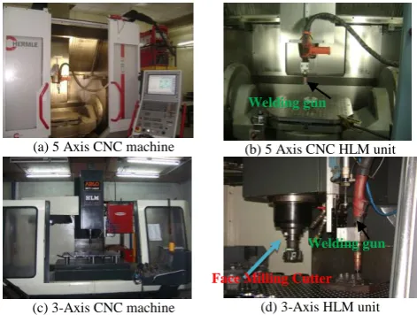
It is computer controlled hybrid RP system that integrates the controlled welding process, which provides the controlled heat and mass transfer and precision control of bead penetration with a CNC end and face milling operation. This deposition makes near-net shape of the object to be built which is then finish machined subsequently. Face-milling is done after depositing each layer to remove oxidized surface and scallops. It also ensures z-accuracy of each layer. This system offers a way of building metallic parts in layered fashion with full density, high mechanical and metallurgical properties, high dimensional accuracy and good surface quality with complex geometrical features and sharp edges [8]. HLM is a 3-/5-axis CNC machine fitted with a MIG weld deposition system, shown in Fig. 2, to do both material addition and subtraction on the same platform.
(a) 5 Axis CNC machine (b) 5 Axis CNC HLM unit
(c) 3-Axis CNC machine (d)3-Axis HLM unit
Fig. 2. Integration of HLM with CNC machines
In contrast in HLM, the focus is on matrix integrity during GMAW deposition and surface quality during machining. As the above competing processes are purely additive they have to use thin layers and hence are slow. HLM, being hybrid, is faster by an order of magnitude as it deposits thick
Welding gun
Welding gun
Gun
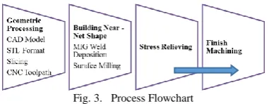
[image:2.595.49.279.635.736.2]layers. Furthermore, HLM is more economical and safer by order of magnitude. The system software developed in-house generates the weld deposition and face milling paths automatically from the CAD model. The stages involved in building the metallic object using HLM is shown in Fig. 3.
Fig. 3. Process Flowchart
III. REALIZATION OF SAMPLE BY HLM TransPulse synergic (TPS) 4000 had been used for deposition of Al-Si alloy (5% Si). The machine is fully automated and by setting the values of thickness of base plate and wire feed rate it automatically adjusts the current and voltage or vice versa. Samples were fabricated in a zigzag deposition pattern with 60 mm long and 20 passes wide, up to a total of 10 layers of 1mm thickness each. Al-Si alloy of wire diameter 1.2 mm was used as welding wire. The width and height of each weld bead were measured and recorded for different input processing parameters to compare and select the optimum deposition parameters.
Typical deposition rates used for these studies were varied. A torch speed in the range of 400 m/min and 1000 m/min was employed. The wire feed rate was pre-programmed based on the input current and it was varied from 3.4 to 4.6 m/min. During deposition of Al-Si alloy, 100% argon was employed as shielding gas at a flow rate of 12 L/min. The main welding parameters in HLM include welding current, step-over increment and torch speed. These parameters were selected based on the following selection criteria:
i. Minimum rate of heat input
ii. Heat distribution over a wider area and higher precision iii. Maximum yield
As shown in table 1, these parameters were tested to observe the quality and geometry of the weld bead to select the optimum parameters to economically build samples for characterization. It was observed that the variation in torch speed mainly affects the weld bead geometry and heat distribution. For high wire feed rate and at high current, weld bead distortion and to the surrounding was observed. If the torch speed is more, the bead is finer and vice-versa as shown in Fig. 4.
(a) Distorted weld bead using high current and lower torch speed
(b) Thin weld bead at lower current & higher torch speed Fig. 4. Weld sizes from different process parameter
An added advantage of higher torch speed is the distribution of heat over a wider area. From the observation
as shown in table 1, the optimum value of torch speed, which is 850 m/min, was taken as a constant value during deposition. Wire speed which is directly related to welding current is an indication of the rate of heat input. In order to minimize distortion, internal stresses and machining allowance, it is desirable to have the lowest possible wire speed. The other important weld parameter is the stepover increment. The optimum value stepover increment as follows [10].
W
P
(
2
/
3
)
*
--- (1) WhereP is for Pitch, W is the weld bead width
As can be seen from the table 1, higher current intensity with lower torch feed and higher wire feed rate will make the shorter and wider weld bead as compare to other combination of the those three affecting parameters. This phenomenon lead to bad weld bead with distorted structure is show in Fig. 5 where lower current intensity and higher torch speed will make a thinner weld bead which is not suitable to for layer additive process due to higher cycle time required.
TABLE I
EXPERIMENTS ON PROCESS PARAMETERS TO FIND OUT THE OPTIMUM VALUE
Current (A)
Torch speed (m/min)
Wire feed rate (m/min)
Bead width (mm)
Bead height
(mm)
Remark
50 400 2.5 3.0 3.0 Good
600 1.6 2.0 Small width
60 650 3.0 2.5 2.5 Good
850 2.0 2.0 Very good
70 700 3.4 3.2 2.5 Very good
850 3.0 2.0 Very good
85 850 4.0 4.0 2.0 Good
1000 3.5 1.8 Very good
90 650 4.1 5.0 2.5 Good
1000 4.0 2.0 Very good
100 600 4.6 6.0 2.5 Good
850 4.5 2.0 Very good
110 600 4.9 7.0 1.8 Bad
1000 5.0 2.0 Good
[image:3.595.306.558.638.784.2]Depending upon the various geometries the parameters were optimized to get a defect free object. Three optimum current values and three wire feed rate related to the current intensities were selected. A total of nine stepover increments were selected by providing the pitch in to three different options as P=1/3W, 2/3W and P=W. Table 2 shows the optimum selected welding parameters.
TABLE 2.
THE SELECTED OPTIMUM PARAMETERS FOR CHARACTERIZATION
Sample Current (A)
Pitch (mm)
Bead width (mm)
Wire feed rate (m/min)
Torch speed (m/min) 1
70
1
3 3.4 850
2 2
3 3
4
85
1.33
4 4.0 850
5 2.66
6 4
7
100
1.5
5 4.6 850
8 3
[image:3.595.45.286.653.745.2]IV. THE EFFECT OF PROCESS PARAMETERS ON TEXTURE AND CRYSTAL ORIENTATION The texture and crystal orientation of Al-Si components, manufactured by HLM, was investigated. The nature and complexity of HLM result in anisotropic properties and objects producing using this technique showed variation in properties because of micro-structural and crystallographic texture variations.
As shown in Fig. 5, the metallographic specimens were sectioned perpendicular to the longitudinal travel direction (X-axis) and perpendicular to the short transverse direction (Y-axis) and mounted and polished in the YZ plane and XZ plane respectively.
An automatic molding machine was used to polish the samples for metallographic analysis. An etchant was prepared to highlight grain morphology. The etchant for Al-Si alloy was prepared with the following composition. Methanol 25ml, Hydrochloric acid 25ml, Nitric acid 25ml and Hydrofluoric acid 1 drop.
(a) Samples build with particular process parameters
(b) The schematic drawings showing welding coordinate system
(c) The effect of increasing pitch during deposition
(d) Etched cross section
Fig. 5. Schematic diagram of deposition
A. Kernel Average Misorientation
The Kernel Average Misorientation (KAM) analysis was done on the top, middle and bottom sections of the sample. Three samples were selected to be tested at each section with different process parameters.
[image:4.595.45.287.295.495.2]EBSD test position for KAM with input deposition parameters is shown in table 3.
TABLE 3
MISORIENTATION ANGLE AT DIFFERENT SECTIONS Sample Position Current Pitch KAM (deg)
3
Top
70 3 0.717
5 85 2.66 0.530
7 100 1.5 0.396
1
Middle
70 1 0.44
4 85 1.33 0.621
8 100 3 0.517
2
Bottom
70 2 0.472
6 85 4 0.451
9 100 4.5 0.622
The KAM at top section showed a decreasing trend with increasing input current but it increase when the pitch increment. However at the middle and bottom sections the KAM an increasing trend with both current and pitch
increment. It was observed that the average KAM was increased as the welding current and pitch increments are increased which is shown in Fig. 6.
(a)Variation of KAM with current (b) Variation of KAM with Pitch Fig. 6. KAM with respect to welding current and stepover increments
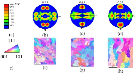
B. EBSD orientation maps and pole figure
Electron Backscatter Diffraction (EBSD) was performed on samples build using HLM. EBSD mapping used a 300 x 600 point grid at 0.4µm steps. Samples were prepared using the optimum process parameters given in table 2. The deposition method and coordinate system of the deposition processes are shown in Fig. 5 (b).
Total 9 specimens were prepared for EBSD analysis by polishing and electronically etched. The specimen with an x-z cross section allows investigation the misorientation and texture of the sample in the specified cross section. The photograph of the sample cross sectioned in x-z plane, showing the top, middle and bottom regions is shown in Fig. 5 (d). As shown in Fig. 7, 8 and 9 the Coloring scheme is a blue-to-red rainbow scale, with blue indicating orientations closest to the reference, red farthest, and the range set by the maximum for the map.
(a) (b) (c) (d)
111
001 101
e) (f) (g)
[image:4.595.316.541.412.536.2](h)
Fig. 7. EBSD pole figures and OM at top portion of the sample (a) Scale for pole figures (e) Scale for OM
(b, f) Sample 3 with Current 70 A, pitch 3 mm, (c, g ) Sample 5 with Current 85 A, pitch 2.66 mm, (d, h ) Sample 7 with Current 100 A,
pitch 1.5 mm
For top portions section testing the samples were made with current variations (70A, 85A and 100A) and pitch increment varied between 1mm and 2.66 mm. The welding current and stepover increments were varied as indicated in the table 3. It can be seen from Fig. 7 that sample a, b and c are showed similar texture intensity towards the rolling direction. Similarly, it can be easily seen that when the current increases from 70A to 100A the intensity of texture is increased in the plane <001>.
level was maximum at the center but as the welding current increases the texture starts to be symmetric with rolling direction axis.
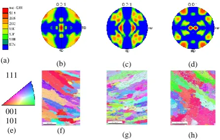
(a) (b) (c) (d)
111
001 101
(e) (f) (g)
[image:5.595.52.276.98.240.2](h)
Fig. 8. EBSD pole figures and OM at middle portion of the sample (a) Scale for pole figures (e) Scale for OM
(b, f) Sample 1 with Current 70 A, pitch 1 mm, (c, g) Sample 4 with Current 85 A, pitch 1.33 mm, (d, h) Sample 8 with Current 100 A,
pitch 3 mm
For bottom portions section testing the samples were made with current variations (70A, 85A and 100A) and pitch increment varied between 2 mm and 4.5 mm. From Fig. 9 it can be easily noticed that the relative variety of colouring in the smaller grains, implying a weaker or non-existent preferred orientation, whereas the larger grains have a reddish shade, indicating a stronger <001> rolling direction texture. In this case the texture showed a fluctuated trend with input welding current and stepover increment.
V. THE EFFECT OF PROCESS PARAMETERS ON MICROSTRUCTURE EVOLUTION
The nature of HLM via welding is similar to multipass welding. The deposited metal is influenced significantly by the additional thermal cycles induced by the deposition of subsequent passes. Only the final pass deposited is un-tempered which remains in primary microstructure. As the microstructure of the build-up comprise of various zones, the overall properties of the weld metal are expected to be determined by the combination of the properties of all of the different zones.
The grain size measurement was carried out on different regions in order to gain a better understanding of the effect
of process parameters on microstructure gradient. Fig. 11 shows the relation between the Process parameters and the size of the fine and coarse grains. Measured microstructure for long and short grains on the coarse and fine regions is shown in table 4.
TABLE 4
CELL SIZE ON COARSE AND FINE GRAIN PORTIONS
Sr. N
o
Printout-microscope mag
Current I (A)
Pitch P (mm)
Coarse Fine
Llc
(µ)
Lsc (µ)
Llf
(µ) Lsf (µ)
1 70 1 79 31 67 18
2 70 2 78 26 67 16
3 70 3 85 18 49 18
4 85 1.33 132 18 58 18
5 85 2.66 117 32 64 14
6 85 4 121 22 64 22
7 100 1.5 103 30 60 16
8 100 3 108 37 78 19
9 100 4.5 119 30 80 24
The microstructure on the fine and coarse regions for I=70 showed relatively small variations between fine and coarse grain sizes. Variation of microstructure with pitch increment is also small. However for higher current inputs of 85A and 100A there is larger variation in microstructure.
This indicates that the optimum processing welding current to get a homogeneous microstructure is 70A but the stepover increment can be varied between 1 and 3mm based on the width of the welding bead. The size of coarse grains firstly increases with increasing current, pitch and then start decreasing slowly as shown in Fig. 10(a).
The size of long grains in the fine region of the microstructure shots up to 80 µm as the welding current increased from 70A to 100A shown in Fig. 10 (b). The effect of pitch showed a slight increase with small fluctuation. A similar fluctuating trend with pitch increment was observed for short size microstructures (Lsc) as shown in Fig. 10(c). The increase in short grain size (Lsf) in fine regions, shown in Fig. 10(d), was less than that of the increase in short grain size (Lsc) in coarse region (c).
(a) Surface plot of longer grains in coarse region
(b) Surface plot of longer grains in fine region
(c) Surface plot of short grains in
[image:5.595.309.553.131.307.2]coarse region (d) Surface plot of short grains in fine region
Fig. 10. The average grain size w.r.t pitch and current on coarse and fine region
In addition to the grain size measurement, microstructure analysis was comprehensively studied. Coarse microstructures were seen towards the bottom of each layer
(a) (b) (c)
(d) 111
001 101
[image:5.595.44.273.443.583.2](e) (f) (g) (h)
Fig. 9. EBSD pole figures and OM at bottom portion of the sample (a) Scale for pole figures (e) Scale for OM
[image:5.595.318.546.582.715.2]whereas fine microstructures were found towards the top of each layer as shown in Fig. 11. Moreover the top layers are naturally air quenched whereas the bottom layers go through slow cooling. This results in a microstructural gradient in the thickness direction. The change in microstructure is the result of multiple reheating of preceding beads by subsequent weld passes.
(a) Fine microstructures at the top of the layers
[image:6.595.314.546.358.567.2](b) Coarse microstructures at the bottom of the layers
Fig. 11. Microstructure at the top and bottom layers
VI. EFFECT OF PROCESS PARAMETERS ON HARDNESS
The same samples, used for metallographic analysis were afterwards used for hardness testing. The hardness was performed using a Hysitron Inc. Minneapolis US, Ti-900 Nano-indenter.
A. Hardness variations in parallel and perpendicular to the weld direction
Nano-indentation testing had been carried out on the weld deposited cross-section on a 10x10 mm matrix both in the horizontal (along the weld direction) and vertical direction (from bottom to top) of the polished face.
(a) A method of 10x10 array for
nanoindentation (b) Hardness from top to bottom layers
(c) Average hardness in parallel and perpendicular to the weld direction
Fig. 12. Nanoindentation methods and results
The mean hardness along Z-axis (from top to bottom layers) shows increasing trend with small fluctuation as shown in Fig. 12(c). It varies approximately from 0.4 MPa to 0.9 MPa. This variation arises due to change in microstructure because of recrystallization of layers due to repeated remelting of the previously deposited layer. It is observed that the hardness at the top of the sample is higher than the hardness at the bottom. The hardness decrease with displacement measured from top to bottom layers as shown in Fig. 12(b).
B. Hardness variation in layers
Hardness variation on top and bottom layers for each sample is measured. These sample manufactured at specific current and pitch. Hardness of each sample measured at top and bottom layers. For better understanding of the influence of cyclic heating on each layer hardness is measured two layer below the top layer and 2 layer above the bottom layer. The hardness measurement was performed with a load of 11,000μN.
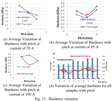
Average hardness variation on top and bottom layer shows a fluctuating trend. For welding current of 70 A hardness decrease with increasing pitch shown in Fig. 13(a). For welding current of 85 A hardness decreases first and then increase with increasing pitch shown in Fig. 13(b). For welding current of 100 A hardness increases first and then decrease with increasing pitch shown in Fig. 13(c). Average hardness variation of at top and bottom layer for all samples is shown in Fig. 13(d). It shows top layer have higher hardness than bottom layer.
From overall results it indicates that current of 70 A and 100A with pitch of 2, 1.5, 4.5 mm will give uniform hardness values at the top and bottom layer, which proves the capability of HLM to produce parts with uniform hardness in the Z-direction
(a) Average Variation of Hardness with pitch at
current of 70 A
(b) Average Variation of Hardness with pitch at current of 85 A
(c) Average Variation of Hardness with pitch at
current of 100 A
(d) Variation of average hardness for all samples with pitch
Fig. 13. Hardness variation
VII. THE EFFECT OF PROCESS PARAMETERS ON RESIDUAL STRESS
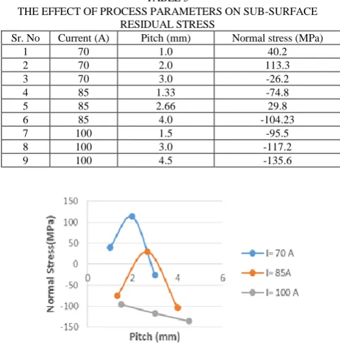
The residual stress changes between tensile and compressive state shown in table 5.
[image:6.595.43.294.413.603.2]TABLE 5
THE EFFECT OF PROCESS PARAMETERS ON SUB-SURFACE RESIDUAL STRESS
Sr. No Current (A) Pitch (mm) Normal stress (MPa)
1 70 1.0 40.2
2 70 2.0 113.3
3 70 3.0 -26.2
4 85 1.33 -74.8
5 85 2.66 29.8
6 85 4.0 -104.23
7 100 1.5 -95.5
8 100 3.0 -117.2
9 100 4.5 -135.6
Fig. 14 Variation of normal stress with pitch
From Fig. 14 it will be seen that it is worthwhile to use welding current of 70A and 85A with pitch of 1 and 3 mm, we will get minimum tensile and compressive residual stress. In general, the fluctuations in residual stresses are due to the differences within the microstructure of a material and repeated thermal cycles. This can be considered as micro residual stress which can change sign and/or magnitude over distances comparable to grain size of the material under analysis.
VIII. CONCLUSION
Characterization of AM components shows that the Kernel Average Misorientation increases with increasing welding current and pitch increments. The texture at the top was found to have similar texture intensity toward the rolling direction. However at the middle of the sample high texture intensity was observed around the center of the pole figures with few portion textured around the periphery of the grain boundaries. The texture at the bottom of the layers showed a fluctuated trend. The size of coarse grains was increased with increasing current. Coarse microstructures were seen towards the bottom of layers whereas fine microstructures were found towards the top of layers. The variation of hardness is more in Z axis than in X axis. The variation of hardness within the layer is more for top layer than bottom layers. The XRD result reveals the presence of compressive and tensile residual stresses in the cross sectioned sample. Compressive stresses in sample varies from 26.2 MPa to 135.6 MPa.
REFERENCES
[1] Suryakumar S., Karunakaran K.P., Bernard A., Chandrasekhar U., Raghavender N., Sharma D., (2011), “Weld bead modelling and process optimization in Hybrid Layered Manufacturing”, Computer-Aided Design, volume 43, pp. 331–34
[2] Bernd Baufeld, Omer Van Der Biest, and Steven Dillien, (2010), “Texture and Crystal Orientation in Ti-6Al-4V Builds Fabricated by
Shaped Metal Deposition” The Minerals, Metals & Materials Society and ASM International, DOI: 10.1007/s11661-010-0255-x
[3] Erhard Brandl, Achim Schoberth, Christoph Leyens, (2012), “Morphology, microstructure, and hardness of titanium (Ti-6Al-4V) blocks deposited by wire-feed additive layer manufacturing (ALM)” Materials Science and Engineering a 532, pp. 295– 307 [4] Tso-Liang Teng, Peng-Hsiang Chang, Wen-Cheng Tseng, (2003),
“Effect of welding sequences on residual stresses” Computers and Structures 81, pp. 273–286
[5] Murr L.E., et.al, (2010), “Characterization of titanium aluminide alloy components fabricated by additive manufacturing using electron beam melting” Acta Materialia 58, pp. 1887–1894
[6] Mishra S.K., Pant P., Narasimhan K., Rollett A.D. and Samajdar I., (2009), “On the widths of orientation gradient zones adjacent to grain boundaries” Scripta Materialia 61, pp. 273–276
[7] Tayon W., Crooks R., Domack M., Wagner J., Elmustafa A.A., (2010) “EBSD Study of Delamination Fracture in Al –Li Alloy 2090” Experimental Mechanics 50, pp.135– 143
[8] Taminger, K.M.B., Hafley, R.A., (2003), “Electron Beam Freeform Fabrication: A Rapid Metal Deposition Process,” Proceedings of the
3rd Annual Automotive Composites Conference, September 9-10, 2003,
Troy, MI, Society of plastics Engineers.
[9] Song, Y., Park, S. and Chae, S. (2005): “3D welding and milling: part II--optimization of the 3D welding process using an experimental design approach”, International Journal of Machine Tools and
Manufacture, Vol. 45(9), pp 1063-1069.
[10] Karunakaran, K.P., Shanmuganathan, P.V., Jadhav, S.J., Bhadauria, P. and Pandey, A. (2000): “Rapid prototyping of metallic parts and moulds”, Journal of Materials Processing Technology, Vol. 105(3), pp 371-381.
[11] Akula, S. and Karunakaran, K. P. (2006): “Hybrid adaptive layer manufacturing: An Intelligent art of direct metal rapid tooling process”,
Robotics and Computer-Integrated Manufacturing, Vol. 22(2), pp
113-123.