Stress effects of silica particles in a
semiconductor package molding
compound
110th European Study Group with Industry,
28th June - 3rd July, 2015
University of Limerick, Ireland
Authors:
Francesc Font1,9
, Graeme Hocking2
, David A. Burton3
, Vincent Cregan4
, Pavel Iliev5
Workshop contributors:
Paul Dellar6
, Shishir Suresh7
, Shaunagh Downing7
, Matthew Haynes1
, Helena Ribera4 , Robert Mangan7
, William Lee1
, Stephen O’Brien1
Industry Representative:
Patrick Elebert8
1
MACSI, Department of Mathematics & Statistics, University of Limerick, Limerick, Ireland
2
School of Chemical and Mathematical Sciences, Murdoch University, Perth, Australia
3
Department of Physics, Lancaster University, Lancaster, UK
4
Centre de Recerca Matematica, Barcelona, Spain
5
University of Sofia, Sofia, Bulgaria
6
OCIAM, Mathematical Institute, University of Oxford, Oxford, UK
7
University of Limerick, Limerick, Ireland
8
Analog Devices, Ireland
9
Summary
Contents
1 Introduction 4
2 Thin strip with variable moisture absorption 5
2.1 Model description . . . 5
2.2 Results . . . 6
2.3 Conclusions . . . 8
3 Numerical simulation for Stress field at epoxy molding-silicon die inter-face 9 3.1 Model description and numerical scheme . . . 9
3.2 Discussion . . . 10
3.3 Conclusions . . . 12
4 2D approximation in the complex plane 13 4.1 Application of the model . . . 15
4.1.1 Axially symmetric solution . . . 15
4.1.2 Asymmetric configuration . . . 16
4.2 Conclusions . . . 18
5 Summary and future work 18 Appendix A Derivation of complex theory elasticity model 20 A.1 Boundary condition at the resin-particle interface . . . 21
A.2 Boundary condition at the resin-loop interface . . . 21
A.3 Fixing the constant β . . . 22
1
Introduction
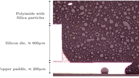
Analog Devices manufacture silicon chips which are used in a variety of circumstances. The chips (or die) do not come as a single entity but have electrodes on top and sit on a copper paddle, all of which is then packaged within plastic. Either the whole thing is encased or alternatively the plastic may be put over the top with the copper paddle as a base (Figure 1). The plastic is an epoxy molding compound that consists of the plastic and up to 90% filler particles that are made of silica.
During manufacture the whole package is heated to a high temperature and then cooled down to room temperature for use. In this process the package is subjected to significant forces as the difference in rates of thermal expansion between the die and the plastic causes the package to bend slightly. This is expected and is a normal part of the process. The purpose of the silica particles is to minimize the effect of the differences in thermal expansion between the two materials. The filler particles are uniformly distributed in the compound and come in a range of sizes, between 50 and 100 microns (Figure 1). To give an idea of scale in the figure, the copper paddle is approximately 200 microns high. After this phase the properties of the chip are adjusted by reconfiguring the electronics to have the required design properties. It is at this point that the chips are shipped for use.
It is apparent that in certain situations the behaviour of the electrical properties of the chip deteriorate in-situ, sometimes leading to bad performance and sometimes to failure. One possible reason for this is thought to be the absorption of moisture into the epoxy compound. It is thought that this leads to a slight further bending (or perhaps unbending) of the package causing further stresses on the chip circuitry, and it is believed that it is the silica filler particles that are the dominant factor in causing problems. Electrical components are susceptible to mechanical stress and so the presence of one or more large silica particles near to the die may lead to changes in the behaviour. It is even possible that a collection of small particles may cause problems.
Analog Devices have performed a series of tests involving the placement of a buffer coating between the epoxy compound and the die to see if this would mitigate the impact of such silica particles. It was found that this coating had to be quite thick before it had any beneficial effect. They also tested the moisture absorption of the plastic compound and found it to absorb water (although the silica particles do not absorb water).
Polyimide with Silica particles
Silicon die,≈600µm
[image:4.595.145.381.501.633.2]Copper paddle,≈200µm
Figure 1: The setup of one end of the chip, showing the copper paddle, the die and the epoxy compound. The silica particles can be clearly seen in the compound as the lighter colour patches.
The study group was asked to investigate this problem by considering the stress field generated by the silica particles so that “a series of Monte Carlo simulations” might be performed by Analog Devices for different distributions of the particles, thus assisting in design of the layout of the chip.
in-sight into the process. The outline of this report is as follows. In Section 2 we describe a model for a two-layer materials problem to consider the effect of variable solid properties on the bending behaviour. Numerical simulations are presented in Section 3. Specifically, the finite element method in COMSOL was used to model the stress field near a bent plate subject to different particle configurations. In Section 4 the problem is approximated via a two-dimensional model and complex variable methods are applied. Finally, in Section 5 we provide some concluding remarks and suggested directions for future work.
2
Thin strip with variable moisture absorption
2.1
Model description
The task to consider the stress generated locally during bending of the chip and casing can be considered by examining the stress field generated by individual particles of silica near to the chip (see later), or it may be considered by looking at a simplified approach in which variations in concentration of the silica particles along the plastic component might affect the bending of the plate. The idea is that as water is absorbed (or heated) the differential absorption along the material will lead to variations in the bending moment, hence causing kinks or regions of higher curvature in the chip itself. Thus we need to develop a model of the curvature due to the absorption of water in a bi-material sheet.
Timoshenko [1] computed bending of two metals welded together with different coeffi-cients of thermal expansion. Subsequently, other authors [2, 3, 4] considered this further, but the essential ideas were covered by [1] and so we use a similar analysis here. In [1] the behaviour of a thermostat with two metal strips welded together was determined. The beams were assumed to be thin and with uniform property along their length. The centre line was assumed to be such that there could be no relative movement between the two strips. While we are not dealing with a bi-metal strip in this work, we still have a very low aspect ratio and so the general assumptions of the model are valid.
One way to interpret his work is to consider it as an analysis of a very small segment of a longer strip pair where the strips have different properties. In that way the expression derived for the curvature can be treated as local. Appending pieces with different prop-erties either side (with an assumption of continuity) leads to a modified equation for the distortion of the strip, one that now has properties that depend on lengthwise direction,
x.
Timoshenko’s formula for the radius of curvatureρas shown in Figure 2 can be written as
1
ρ =
2h(α1−α2)(T −T0)
h2+ 4(E
1I1+E2I2)
1
E1h1 + 1
E2h2
, (1)
where in layers k = 1,2, αk is the thermal expansion coefficient, EkIk is the flexural
rigidity and hk is the layer thicknes. Temperature, T, is assumed uniform throughout
both layers and h = h1+h2 is the total thickness. He used this model to compute the
bending due to the differential in thermal expansion between the two layers.
Modifying his analysis to consider continuous variations in material properties along the strip allows the development of an equation for the variations in behaviour of the two materials. For example, the two thermal expansion coefficients can be made a function of x, leading to differential bending along the strip. This change leads to a differential equation for the bending of the strip, given by
d2
y dx2 =
2h(α1(x)−α2(x))(T(x)−T0)
h2+ 4(E
1I1+E2I2)
1
E1h1 + 1
E2h2
, (2)
1 1
E ,I
2 2
,α
,α
1
2
[image:6.595.169.428.56.172.2]E ,I
Figure 2: Sketch of the bending due to differential thermal expansion during heating or moisture absorption in two layers welded together. E is Young’s mod-ulus, I is moment and α is the thermal expansion coefficient.
also affect the rigidity, but for now we assume this effect is minor.
This equation can be integrated to compute the variation in bending as the strip heats (or cools). Indeed, it may be possible to estimate the differential between α1 and α2
at any point by examining the outcome of the manufacturing process. Two boundary conditions are required to enable a solution to this equation, but they can simply be set toy(0) =y(1) = 0 since in this problem they are not of great importance. It would seem likely in this application that the variation in the paddle would be much less than the plastic, as the paddle is made of a single material while the plastic has two constituents. The variation inα1(x) is likely to be due to the location and density of the silica particles
and related to the local volume fraction that they occupy, while α2 can be expected to
remain almost constant. The length scale of these variations might be expected to be of the order of the larger particles, but could also be due to a dearth or excess of particles in one particular location.
In the problem under consideration it is the moisture content that is of concern. The epoxy will absorb moisture resulting in an expansion of the material and subsequent bending. This will lead to the same kind of variation as one might expect from the cooling process, depending on the amount of expansion and the volume occupied by the silica.
Following the same derivation as for the thermal equation, we can arrive at a similar equation for the moisture induced bending, where the terms involvingαkare replaced by
a moisture interaction of the form β1(x)(W1−W10)−β2(x)(W2−W20), where βk, k =
1,2 is the expansion factor as water is absorbed and Wk0, k = 1,2 is the initial water
concentration in each component. However, since we do not expect the copper to change, this term in layer 2 will disappear, giving
d2
y dx2 =
2hβ1(x)(W1(x)−W10)
h2
+ 4(E1I1+E2I2)
1
E1h1 + 1
E2h2
, (3)
if we assume that the presence of the moisture has no influence on the other properties of the components. In fact, it is relatively simple to include the variation of the properties if we know the relation, but it is unlikely that it will be of sufficient magnitude to change the results. The moisture term can be replaced by
B(x) =β1(x)(W1(x)−W10),
to test whether it is likely to make a difference, since it is simply a function of x that is related to the volume fraction of silica along the epoxy layer.
2.2
Results
0 0.2 0.4 0.6 0.8 1 0
0.002 0.004 0.006 0.008 0.01 0.012 0.014
X
Vertical displacement
Moisture absorption rate
(a)
0 0.2 0.4 0.6 0.8 1
0.002 0.004 0.006 0.008 0.01 0.012 0.014
X
Vertical displacement
Moisture absorption rate
(b)
0 0.2 0.4 0.6 0.8 1
0 0.002 0.004 0.006 0.008 0.01 0.012 0.014
X
Vertical displacement
Moisture absorption rate
[image:7.595.90.495.204.550.2](c)
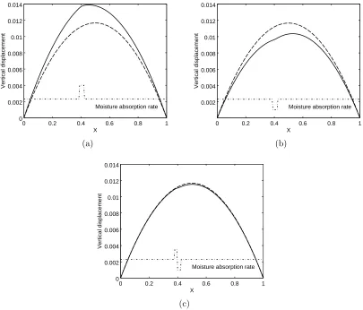
Figure 3: Comparison of three cases of variable moisture uptake along the epoxy side of the component. The dot-dash line indicates the variation in moisture. The dashed line gives the bending for the uniform case and the solid line is the result of the variable moisture uptake (due to the variation in silica concentration). Other parameters; E1= 18 GPa, E2 = 120 GPa, h1 = 0.008 m, h2 = 0.001 m and
I =h3
0 0.2 0.4 0.6 0.8 1 0
0.002 0.004 0.006 0.008 0.01 0.012 0.014
X
Vertical displacement
[image:8.595.197.382.63.212.2]Moisture absorption rate
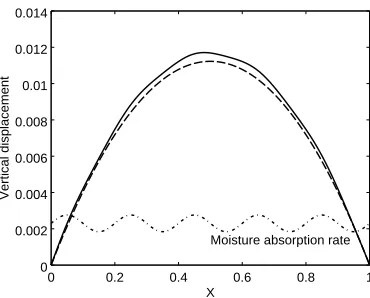
Figure 4: Distortion due to sinusoidal variation in the moisture expansion rates. The plate is now quite “wobbly”.
uniform situation. In frame (a), there is one patch where there is a dearth of silica, so that the expansion coefficient is higher causing greater curvature at that point. The extra bending causes a greater arc in the whole system, but that is due to the sharpish corner that develops. In frame (b), there is a region of lower shrinkage (high silica region) close to x = 0.4, and a narrow region of high absorption. On this occasion the non-uniform case has slightly less bending but a slight kink in the shape is clear. Finally, in frame (c) is shown an example in which the paucity and excess regions are next to each other (as might happen if there were some repositioning of the silica in the manufacturing process). In this case the change in shape is quite localized to this region, but involves the formation of a rather severe kink in the system.
In a final example (Figure 4) we consider a rather extreme case in which there is some continuous variation in the density of silica along the bi-material. Here the variation in expansion is causing some quite nasty kinks to form. It is possible that shorter wavelength inconsistencies can cause more dramatic bending.
2.3
Conclusions
These examples show that if there is variation in the volume fraction along the length of the coating it may result in extra stresses on the chip itself due to this extra, localized bending. The variation may be caused by near proximity of several large particles thus causing an increased local concentration of silica. It is also worth noting that any effect due to this will occur in the same place in both the cooling phase during manufacture and in any subsequent moisture absorption. While the “damage” done during manufacture can be repaired, it is not possible to repair the later damage due to moisture absorption. It is even possible that given the right circumstances the two effects could be additive, even though the process of cooling and moisture absorption would result in bending in the opposite directions.
will be necessary to return to the more time consuming calculation of the stresses due to individual particles.
3
Numerical simulation for Stress field at epoxy
molding-silicon die interface
3.1
Model description and numerical scheme
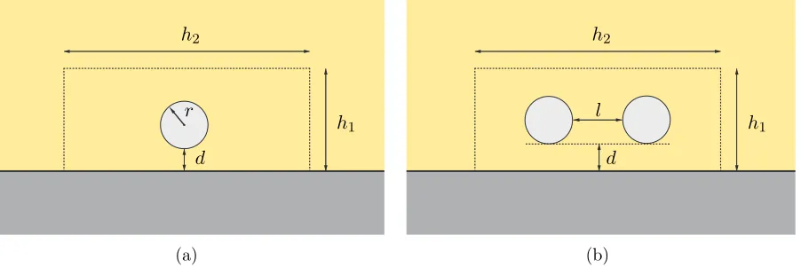
In this section we use the finite element method (FEM) in COMSOL to analyse and simulate the stress near the interface of the epoxy molding and the silicon die as a result of the silica particles embedded in the molding. We consider a two-dimensional, stationary model to predict the stress field. Two different particle configurations are studied. Firstly, in case A (Figure 5(a)) we investigate the relationship between one particle and the stress in the molding. Next, in case B we examine the impact of two particles on the stress field (Figure 5(b)).
The starting point is the construction of the problem geometry. The domain consists of two subdomains, namely a rectangle for the molding and a circle for the silica particle. As illustrated in Figure 5 the yellow area represents the molding compound, the light grey circle a silica particle and the dark grey area the silicon die. The simulation domain is the rectangle delimited by the dashed line. The height and length of the rectangle are
h1 = 1000µm and h2 = 5000µm, respectively. The Cartesian coordinate system is used
to describe the problem with the geometry aligned such that the length is described along
x∈ [−h2/2, h2/2] and the height y ∈[0, h1]. The radius of the particle is r = 25µm. In
both configurations,drepresents the vertical distance from the base of the rectangle to the lowest point on the surface of a particle. With respect to case B,l denotes the horizontal distance between two particles. The COMSOL materials library is used to define the material properties of both the molding and silica particles. For the molding we use the materialEpoxy-50% silica particles to approximate the molding used by Analog Devices. A summary of the physical dimensions and material parameters is given in Table 1.
Quantity Symbol Value Units
Molding height, length h1,h2 1×10− 3
, 5×10⁻³
m
Particle radius r 2.5×10⁻⁵
m Young’s modulus of epoxy, silica Ee, Es 72.9×10
9
, 18.03×10⁹ Pa Poisson ratio of epoxy, silica νe, νs 0.17, 0.23
-Density of epoxy, silica ρe, ρs 2203, 1100 kg m−
3
Table 1: Dimensions of geometry and material properties of molding compound (Epoxy-50% silica particles) and silica used in simulations.
To reduce model complexity we use the following assumptions. Firstly, we simplify the geometry of the problem by neglecting the die and copper paddle located at the base of the molding. We assume that both the molding and silica particles are linear elastic materials such that strains vary linearly with stresses.
We use the solid mechanics module in the structural mechanics package to simulate the stress field. The governing equations are
−∇ ·σ =FV , σ=s, s=C: (ǫ−ǫinel), ǫ=
1 2[(∇u)
T +∇u], (4)
where σ is the Cauchy stress tensor, FV is the body force per unit volume, ǫ is the
(a)
r
d
h1
h2
(b)
d
h1
h2
[image:10.595.75.526.58.213.2]l
Figure 5: Sketch of case A and case (b). The yellow area represents a portion of the molding compound (Epoxy-50% silica particles), the light grey circle a silica particle and the dark grey area the silicon die. The simulation domain is represented by the rectangle delimited by the dashed line.
which is an expression of Newton’s second law. The third equation is Hooke’s law, which relates the unknown stresses and strains.
Boundary conditions are required at the four outer edges of the molding and the particle-molding interface. At x =−h2/2, x =h2/2 and y =h1 we impose free
bound-ary conditions so that there are no constraints or loads acting on the boundbound-ary. At the particle-molding interface we apply stress continuity. Finally, in order to model the bending caused by the the moisture absorption in the epoxy, we impose a prescribed dis-placement condition of the formu=−εx2
at the lower surface of the molding,y= 0. The small, dimensionless parameter ε = 1×10⁻¹⁰
determines the magnitude of the overall displacement of the molding.
The next step is the discretisation of the original problem which consists of trans-forming the continuum problem as represented by the partial differential equation model into a discrete problem in finitely many variables. The domain is subdivided into finite elements of variable size and shape which are interconnected by a finite number of nodal points. COMSOL automatically partitions the domain into small finite elements of simple shape. The resulting partition is referred to as the finite element mesh (Figure 6). In two dimensions the mesh subdivides the domain into triangles. However, this is only an ap-proximation as part of the domain close to the particle is curved. The sides and corners of the triangles are called mesh edges and mesh vertices, respectively. In each finite element the unknown stress is approximated by some low order interpolating polynomial in such a way that the stress is defined in terms of the approximate stresses at the vertices. For the current problem COMSOL used a mesh of 7156 elements. This mesh size was selected as successive, finer meshes showed no significant change predicted stress.
We performed simulations for the one and two particle configurations. We chose the parameter sweep option to simulate the stress field for varying molding parameters. Specifically, for case A the simulation was carried out several times for different values of
d. For case B, dwas fixed and simulations for varyingl were performed.
3.2
Discussion
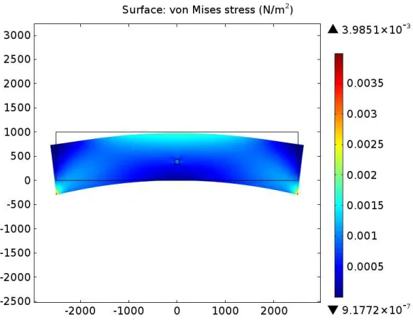
The results from the simulations are shown in Figures 7-11. Figure 7 shows the stationary stress field in the molding for one silica particle. The largest stresses are located near the edges of the molding at x = −h2/2 and x = h2/2. These high stresses are due to the
displacement boundary condition, u = −ǫx2
Figure 6: FEM mesh for domain with one particle. The mesh consists of 7156 mesh elements and was constructed systematically using COMSOL’s mesh mode.
we neglect the stress field near the edges of the molding.
[image:11.595.151.442.304.531.2]COMSOL 4.3.2.152
Figure 7: Stress field in molding subject to one particle.
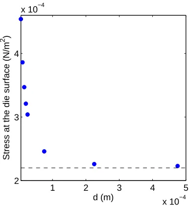
Figure 8 shows the stresses for case A near the centre of the molding along y = 0. The different coloured curves denote solutions for varyingd. In particular, we performed simulations for d = 5µm (blue), 10µm (green), 15µm (red), 20µm (cyan) and 25µm (magenta). Figure 8 reveals that the stress decays rapidly for increasing values ofd. This fact is corroborated by Figure 9 which shows the stress at the origin for varyingd. Smaller values ofdlead to higher stresses.
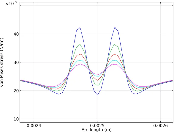
The stress field for case B near the centre of the molding along y = 0 is shown in Figure 10. The coloured curves represent solutions for fixed d = 5 m and varying l. We carried out simulations for l= 5µm (blue), 30µm (green), 55µm (red), 80µm (cyan), 105µm (magenta), 205µm (yellow) and 505µm (black). The graph suggests that in each case the highest stresses at the die-molding interface are located directly beneath the particles. Figure 11 illustrates the stresses for case B alongy= 0. The horizontal distance between the two particles is fixed atl= 10 m, anddis varied such thatd= 5µm (blue), 10µm (green), 15µm (red), 20µm (cyan) and 25µm (magenta). Again we note that as
Figure 8: Stress field at the interface between the molding compound and the silicon die aty= 0 ford= 5µm (blue), 10µm (green), 15µm (red), 20µm (cyan) and 25µm (magenta).
1 2 3 4 5
x 10−4 2
3 4
x 10−4
d (m)
Stress at the die surface (N/m
2 )
Figure 9: Stress at the central point of the interface as a function of d. The first five points on the left represent the plots from Figure 8. The remaining three points correspond to larger values of d. The black line is the stress experienced when the particle is removed.
3.3
Conclusions
In this section we presented numerical simulations for a simple two-dimensional geometry that approximates the qualitative behaviour of the semiconductor and molding compound used by Analog Devices. Neglecting the stresses near the edges x=−h1/2 andh1/2, we
[image:12.595.197.390.357.567.2]Figure 10: Stress created at the interface by the presence of the two silica parti-cles. For this simulations the particle-interface distance is fixed at d= 5µm and the separation between particles is l = 5µm (blue), 30µm (green), 55µm (red), 80µm (cyan), 105µm (magenta), 205µm (yellow) and 505µm (black).
Figure 11: Stress created at the interface by the presence of the two silica particles. In this case the separation between particles is fixed at l= 10µm and the particle-interface distance is d = 5µm (blue), 10µm (green), 15µm (red), 20µm (cyan) and 25µm (magenta).
intermediate layer separating the silicon chip and the molding compound.
4
2D approximation in the complex plane
[image:13.595.152.445.371.593.2]most striking application of this approach is the study of vortex dynamics; analytic contin-uation and conformal mapping techniques have played significant roles in highly efficient calculations of the dynamical evolution of vorticity [6], and the fluid forces exerted by vortices, in a vast array of domains with non-trivial geometries and topologies (see, e.g., [7, 8]). It is perhaps less well-known that such techniques can be fruitfully brought to bear on problems in elasticity theory, as first demonstrated by Kolosov and Muskhel-ishvili in 1909 (see [9] and references therein). The strategy that we follow here is inspired by their treatment of elasticity in the complex plane, as presented in Ref. [9], but with modifications that accommodate thermal stress.
The purpose of these notes is to explore the thermo-mechanical response of a simple idealised system that captures a flavour of the full problem and is amenable to analytical investigation. We represent the silica particle as a disc in the complex plane and embed the disc in a finite medium representing the resin. The Lam´e parametersλ,µ, the coefficient of thermal expansion α and the temperature T of the resin are constant. A thin elastic loop, with Young’s modulusE, bounds the resin-particle composite and, for simplicity, we neglect the shear forces within the loop. For convenience, we suppose that the composite loop-resin-particle system has finite thickness h (out of the plane) and endow the loop with a rectangular cross-section. The area of the cross-section of the loop is A = hw, where the width w of the cross-section is much less than the other length scales in the system, and we will capture the presence of the chip by allowing the product EA to depend on position within the loop. Of course, we do not permit any element of the loop-resin-particle system to deform out of the plane and, furthermore, the loop and the silica particle are both assumed to be inert to changes in temperature. We suppose that the silica particle is rigid when compared to the resin, and set the displacement of the resin to zero at its interface with the silica particle. We also appropriately balance the contact forces at the interface of the loop and the resin.
The small deformation of the composite system due to a change in temperature can be found by solving
−i(κ+ 1)Ω(Z)−2µD+βZ= T
h dZ
ds , (5)
for the function Ω(z), which is chosen to be analytic within the region bounded by the loop. The simple closed curvez=Z(s) specifies the state of the undeformed loop, where
sis the arc parameter of the undeformed loop. The functionD(s) is the displacement of the outer component of the boundary of the resin and has the form
2µD=κΩ(Z)−ZΩ′(Z)−κΩ
a2
Z−c +c
+
a2
Z−c+c
Ω′(Z), (6)
and the tensionT in the loop satisfies
T(s) =EA(s) Re
dZ
ds dD
ds
, (7)
where the elastic properties of the loop at the material point s are specified by EA(s). The centre of the silica particle is located atz=candais the radius of the particle. The material constant κof the resin is
κ= 3−4ν , (8)
where the Poisson ratio ν of the resin satisfies
λ
µ =
2ν
1−2ν. (9)
The response of the resin to changes in temperature is determined byβ where
β=−(λ+µ)α(T −T0), (10)
withT the temperature of the resin andT0 the reference temperature.
We will now turn to the analysis of (5), (6) and (7) for a simple choice of Z(s) and
Figure 12: The silica particle (light grey) is represented by a rigid disc, and the resin (dark grey) is represented by a homogeneous isotropic thermo-elastic medium. An elastic loop (black curve) interfaces with the outer component of the boundary of the resin and captures a flavour of the presence of the chip (the black dot on the right marks the centre of the chip). The silica particle and loop are assumed to be inert to changes in temperature.
Figure 13: The axially symmetric configuration.
4.1
Application of the model
As we will now show, a perturbative analysis of (5), (6) and (7) for the configuration shown in Figure 12 yields a relatively simple analytical expression for the inhomogeneity in the tension due to the presence of the chip and the stresses due to the silica particle. It is vital to note that our model only allows the chip to sense the particle via interaction with the resin; it does not account for stresses that arise if the silica particle makes direct contact with the chip.
4.1.1 Axially symmetric solution
The simplest non-trivial solution to (5), (6) and (7) arises when the silica particle occupies the inner region of an annulus of resin (Figure 13) and the productEAis constant; thus,
c= 0 and the loop is a circle whose centre is at the origin (for all values of the temperature
T). The undeformed loop has radiusband, sincesis the arc parameter of the undeformed loop, it follows
Z(s) =bexp(is/b). (11)
The function Ω(z) is chosen to be analytic inside the closed contour Z as part of the derivation of (6) and, using Z(s) = b2
/Z(s), inspection of (6) shows that D can be expressed as a Laurent series inZ. In particular, a purely radial deformation is described by1
D = δ1Z where Im(δ1) = 0, and Ω(Z) =α1Z follows from (6). Since Im(T) = 0 it
1
[image:15.595.243.352.285.393.2]follows that (5), (6), (11) yield Im(α1) = 0 and
(χ−1)2µδ1+ (κ+ 1)α1 =−β, (12)
2µδ1 = (κ−1)(1−ε 2
)α1, (13)
where
ε= a
b, (14)
χ= EA
2µhb. (15)
Equation (7) leads toT =EA δ1 and solving (12), (13) forδ1,α1 gives
T =−EA
2µ
(κ−1)(1−ε2
)β
(κ−1)[χ(1−ε2
) +ε2
] + 2. (16) Finally, using (8), (9) and (10) to eliminateκ,β yields the expression
T = EA 2
1−ε2
(1−2ν)[χ(1−ε2
) +ε2
] + 1α(T −T0), (17) for the tension in the loop.
It is worth noting that an approximation to (17) can be obtained using simple physical reasoning. According to Hooke’s law, the tension in the loop is T = EA∆l/l where ∆l
is the increase in circumference of the loop due to the thermal expansion of the resin and l is the circumference of the loop in the undeformed state. Let r be the radius of the loop in the deformed state; thus 2πr = l+ ∆l. The change in volume ∆V of the resin is related to temperature as follows: ∆V = π(b2
−a2
)hα(T −T0). However,
∆V=π(r2
−a2
)h−π(b2
−a2
)hand combining the previous two expressions for ∆V with
r=b+ ∆rleads to ∆r=b(1−ε2
)α(T−T0)/2 to first order in ∆r. SinceT =EA∆l/l=
EA∆r/b the result T = EA(1−ε2
)α(T −T0)/2 follows immediately. The additional
terms in the denominator of (17) are a consequence of the back-reaction of the stretched loop on the resin; the above simple argument does not include the stress exerted by the loop on the resin in the deformed state.
An immediate consequence of (17) is dT/dε2
< 0, because Poisson’s ratio ν must satisfy ν < 1/2, which is reassuring because the loop and the silica particle are inert under changes in temperature and less resin should lead to a lower tension.
4.1.2 Asymmetric configuration
It is straightforward to obtain the tension in the loop when the centre of the silica particle is a small distance from the centre of the circular loop in the undeformed state (Figure 12). We suppose that Ω(z) =ξα0+α1z+ξα2z
2
+O(ξ2
) where the real dimensionless parameter
ξ has been introduced to easily distinguish the perturbations, and we also replace cwith
ξcin (6). We will set ξ to unity at the end of the calculation.
Without loss of generality we can set Im(c) = 0 and choose c >0. It follows that
a2
Z−ξc +ξc=ε
2
Z+ξc
1 +ε2Z
2
b2
+O(ξ2), (18) whereε=a/bas before. Hence
Ω
a2
Z−ξc+ξc
=ξα0+α1
ε2
Z+ξc
1 +ε2Z 2
b2
+ξα2ε 4
Z2
+O(ξ2
), (19)
and, usingZ =b2
/Z, inspection of (6) then shows that
D=ξδ0+δ1Z+ξδ2Z 2
where δ0, δ1,δ2 are constants. The constant δ0 is a uniform displacement and does not
contribute to the tension of the loop, so we will not consider it further. We addressed the constants δ1, α1 in Section 4.1.1 and the only important new information concerns the
constantsδ2,α2. Thus, the remainder of this section is focussed on determining δ2,α2.
For simplicity, we will begin by assuming that EA is constant; we will introduce a modulation inEA that captures the presence of the chip at the end of this section. Note that the tension can be written as
T =EARe(δ1+ξ2δ2Z) +O(ξ 2
) =EA(δ1+ξδ2Z+ξδ2b
2
/Z) +O(ξ2
), (21)
using (7), (20), |dZ/ds|= 1, Z = b2
/Z, Im(δ1) = 0. Hence, equating coefficients of ξZ 2
in (5), (6) leads to
EA δ2 =−hb[(κ+ 1)α2−2µδ2], (22)
2µδ2 =κ(1−ε 4
)α2−c(κ−1)
ε2
b2α1. (23)
Solving (22), (23) forδ2,α2 and using the results to eliminate δ2 inT gives
T =T0
1−c
b
8ε2
(1−ν) (1−ε2
){(3−4ν)[χ(1−ε4
) +ε4
] + 1} cosθ
, (24)
whereO(ξ2
) terms have been discarded prior to settingξto unity andθ=s/bis the angle from the real axis in the anti-clockwise sense. The constant T0 =EA δ1 is the tension in
the loop when c = 0 (i.e. that given in (17)), the constant χ is given in (15), Poisson’s ratio ν has been introduced using (8), and (11) has been used to show the point-wise dependence of (24). Since the parameters in (24) satisfy ν < 1/2, χ > 0, 0 < ε < 1,
c/b > 0 it follows that the tension at θ = 0 is less than the tension at θ = π. This is intuitively reasonable because there is more resin to the left of the particle than to the right of the particle (Figure 12).
It is straightforward to capture a flavour of the presence of the chip by modulating the elastic parameterEA of the loop as follows:
EA(s) =EA0(1 +γcosθ), (25)
whereEA0 is a constant and θ=s/b. The centre of the chip is located ats= 0 and the
constant γ in (25) satisfies γ > 0 to ensure that θ = 0 is a maximum of EA. Equation (25) can be written as
EA(s) =EA0[1 +γ1Z(s) +γ1b 2
/Z(s)], (26)
where 2bγ1 =γ, and a repetition of the previous analysis withγ replaced by ξγ leads to
the modification
EA0(δ2+γ1δ1) =−hb[(κ+ 1)α2−2µδ2], (27)
of (22). Solving (23), (27) for δ2,α2 then leads to
T =T00
1−8ε
2
(1−ν)c/b−γ[1 + (3−4ν)ε4
](1−ε2
) (1−ε2){(3−4ν)[χ
0(1−ε4) +ε4] + 1}
cosθ
, (28)
where
χ0 =
EA0
2µhb, T00= EA0
2
1−ε2
(1−2ν)[χ0(1−ε2) +ε2] + 1
α(T−T0), (29)
and, as before,O(ξ2
Since ν <1/2, χ0 > 0, 0 < ε < 1, inspection of (28) shows that the denominator of
the coefficient of cosθ is positive. However, unlike (24), the numerator has an indefinite sign because the influence of the chip and the proximity of the silica particle contribute to (28) with opposite signs (recall γ > 0, c >0). It follows that a choice of parameters exists for which the inhomogeneity in the tension vanishes; the optimum position c∗ of the silica particle for which this occurs is
c∗ = bγ[1 + (3−4ν)ε
4
](1−ε2
) 8ε2
(1−ν) . (30)
4.2
Conclusions
We have developed an efficient model of a thermo-mechanical composite system that captures a flavour of the full problem. Our results are compatible with the notion that less resin is associated with lower stress and the position of the silica particle can be chosen to render the stress in the chip uniform. Although our results are intuitively reasonable, we caution that they are based on a perturbative analysis and Hertzian contact stresses between the particle and the chip are not included. We also caution that our model of the chip is somewhat crude and also does not accommodate shear forces. It can be shown that the above results are insufficient for deducing the curvature of the deformed loop (which could be used to estimate the magnitude of the shear forces in the chip) because the perturbative analysis needs to be carried through to at least second order inξ for this purpose.
5
Summary and future work
The aim of this report was to use mathematical techniques to assist Analog Devices in developing an understanding of the stresses in a silicon chip encased in an epoxy compound due to moisture absorption and the presence of silica particles in the compound. Several different modelling approaches were considered and these will form the basis of future inquiries.
In Section 2 the stress field in the system was approximated by considering a model for the curvature due to the absorption of water in a bi-lateral sheet. The model of Timoshenko [1] was adapted to the current problem to obtain a differential equation for the vertical displacement of the strip due to thermal expansion (or equivalently absorption of water). This bulk approach was easy to implement and did not require time consuming simulations. It showed that variation in silica concentration along the length of the coating can result in extra stresses on the chip due to bending. Further work could test to what extent this variation exists in the epoxy coating and how much would be required to cause the observed damage.
In Section 3 the FEM was used to study the stress field near the epoxy molding-die interface for a reduced two-dimensional case. We have identified three possible extensions to the analysis which can be considered in future studies:
1. The largest stresses were found to be directly beneath the particles near the interface. These stresses were shown to decay very rapidly as the particles were moved away from the interface. Further analytical modelling is required to elucidate the nature of this rapid decay. Indeed, understanding this phenomena in detail would provide invaluable insight on the optimal size of the intermediate layer separating the silicon chip from the molding compound.
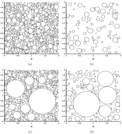
randomly distributed particles are shown in Figure 14. For example, Figures 14(a) and 14(b) correspond to geometries containing 1000 and 100 particles, respectively. Figures 14(c) and 14(d) show geometries where the maximum particle size was in-creased. Running COMSOL simulations using this geometries would provide a more realistic description of the actual process.
3. The bending of the epoxy compound was modelled by imposing a quadratic dis-placement at the lower boundary of the domain. This simplification was necessary to make the model tractable in the short term. In a future study, introduction of bending via a physics-based approach will make the model more representative of the actual system. In fact, COMSOL has a solid mechanics module that allows one to include thermal expansion. This would allow one to introduce bending into the model in a more realistic way.
0 0.5 1 1.5 2
0 0.2 0.4 0.6 0.8 1 1.2 1.4 1.6 1.8 2 x (a)
0 0.5 1 1.5 2
0 0.2 0.4 0.6 0.8 1 1.2 1.4 1.6 1.8 2 x (b)
0 0.5 1 1.5 2
0 0.2 0.4 0.6 0.8 1 1.2 1.4 1.6 1.8 2 x (c)
0 0.5 1 1.5 2
[image:19.595.96.496.241.680.2]0 0.2 0.4 0.6 0.8 1 1.2 1.4 1.6 1.8 2 x (d)
Figure 14: Particle geometry for (a) 1000 particles (b) 100 particles with mini-mum radius of 0.0001 and maximini-mum radius of 0.1 and for (c) 400 particles and (d) 100 particles with minimum radius of 0.01 and maximum radius of 0.5. (Graphs were generated using dimensionless quantities.)
Moreover, the position of the silica particles can be selected such that the stress in the chip becomes uniform. In a future study the model should be extended to include shear forces and Hertzian contact stresses between the particle and the chip.
The problem presented by Analog Devices proved to be demanding due to the inho-mogeneity of the materials involved, and the group worked hard to come up with several different possible approaches that may lead to further progress. It is quite likely that pursuing one or more of these will lead to an answer to the questions posed.
A
Derivation of complex theory elasticity model
The stress tensor σjk of the resin is
σjk =µ(∂juk+∂kuj) + λ∂lul+β
δjk, (31)
where j, k = 1,2, and the vector u(x, y) = u1(x, y) ˆx+u2(x, y) ˆy is the displacement
of the infinitesimal element of resin located at (x, y) in the undeformed configuration. Furthermore, uj =δjku
k where δjk is the Kronecker delta and the Einstein summation
convention has been used.
Following the strategy in Ref. [10], the form of the constant β in (31) is fixed by demanding thatσjk vanishes for a finite element of resin that is allowed to expand freely
due to an increase in temperature. The expression for β is sensitive to the dimension of the ambient space; our model is constrained to 2 dimensions whereas the analysis in Chapter 1 of Ref. [10] admits thermal expansion in 3 dimensions. Thus, the expression in Ref. [10] corresponding toβ will not agree with our analysis here; we will determine the form ofβ at the end of the Appendix.
Navier’s equation
µ[∇2
u+∇(∇·u)] +λ∇(∇·u) = 0, (32) follows from the local equation of momentum balance ∂jσjk = 0 and (31). Introducing
z = x +iy and the complex displacement D(z, z) = u1(x, y) +iu2(x, y) leads to the
following:
ˆ
x·∇(∇·u) +iyˆ·∇(∇·u) = 2∂z¯(∂zD+∂zD), (33)
ˆ
x· ∇2
u+iyˆ· ∇2
u= 4∂¯z∂zD , (34)
and (32) can be written as
4µ∂¯z∂zD+ 2(λ+µ)∂z¯(∂zD+∂zD) = 0. (35)
Inspection of (35) immediately leads to
4µ∂zD+ 2(λ+µ)(∂zD+∂zD) =φ′(z), (36)
where the unknown function φ(z) has been introduced via its derivative for later conve-nience.
Equation (36) and its complex conjugate can be solved for ∂zD and the result used
to eliminate∂zD from (36). Introducing Ω(z) = (λ+µ)φ(z)/[4(λ+ 2µ)] in the resulting
expression for ∂zDyields
2µ∂zD=κΩ′(z)−Ω′(z), (37)
whereκ is given in (8). The complex displacement
2µD(z,z¯) =κΩ(z)−zΩ′(z)−ω(z), (38)
Note that (38) is the general solution to (35) and the unknown functions Ω(z) andω(z) must be fixed by the boundary conditions. The displacement is chosen to vanish at the interface between the resin and the silica particle and this will allow us to eliminateω(z) (we will return to this point shortly).
As noted in Section 4, it is convenient to endow the resin with a finite height h out of the plane and, from this perspective, a curve in the complex plane is equivalent to a ribbon of height h. The contact force per unit area fj exerted at a point on the resin by
the elastic loop is fj = σjknk, where the unit normal nk points towards the loop. The
boundary condition that we will use to determine Ω(z) is given by the requirement that the contact force per unit area exerted by the resin on the elastic loop must be equal and opposite to the contact force per unit area exerted by the loop on the resin. Expressing
σjk in terms of the complex displacement leads to
σ11+σ22= 2(λ+µ)(∂zD+∂zD) + 2β, (39)
σ11−σ22= 2µ(∂zD+∂zD), (40)
σ12=iµ(∂zD−∂zD), (41)
which, combined with (38), yield
σ11+iσ12= Ω′(z) + Ω′(z)−zΩ′′(z)−ω′(z) +β, (42)
σ22−iσ12= Ω′(z) + Ω′(z) +zΩ′′(z) +ω′(z) +β. (43)
The geometry of the outer component of the boundary of the resin is specified by the simple closed curve z =Z(s) where s is the arc parameter of the curve, and we choose
Z to be oriented in the anti-clockwise sense. The tangent to the curve is dZ/ds and it follows that the outward-pointing normal isn=−idZ/dswheren=n1+in2. Using (42),
(43) with fj =σjknk yields the remarkably compact expression
f =−id ds
Ω(Z) +ZΩ′(Z) +ω(Z) +βZ ,
, (44)
for the force per unit area exerted by the elastic loop on the resin, wheref =f1+if2.
A.1
Boundary condition at the resin-particle interface
For simplicity, the silica particle is assumed to be rigid in comparison with the resin and the elastic loop. Thus, the displacement (38) must vanish on the curve (z−c)(z−c) =a2
where c is the centre of the particle and a is the radius of the particle. A simple way to enforce this condition is to analytically continue Ω into the disc occupied by the silica particle and choose
ω(z) =κΩ
a2
z−c +c
−
a2
z−c+c
Ω′(z). (45)
Note that Ω(z) is chosen to be analytic everywhere within the outer component of the boundary of the resin, i.e. within the simple closed curvez=Z(s).
A.2
Boundary condition at the resin-loop interface
The width of the cross-sections of the elastic loop are assumed to be much less than the other length scales in the system. Thus, for simplicity, we identify the outer component of the boundary of the resin with the space curve representing the loop and neglect shear forces within the loop. The loop then satisfies the balance law
dN
associated with an elastic string (see, e.g. [11]) and the contact forceN is given by
N =T ddR
ds , (47)
where T is the tension in the loop, R(s) is the space curve describing the shape of the loop,s is the arc parameter of the loop in the undeformed state and
ddR
ds =
1
|dR/ds|
dR
ds. (48)
The tension is specified in terms of the stretch |dR/ds| and we will adopt the simplest choice: the linear stress-strain relationship
T(s) =EA(s)dR
ds −1 , (49)
where the loop has Young’s modulus E and A(s) is the area of the cross-section of the loop labelled bys. The vectorF in (46) is the force per unit reference length exerted on the loop by the resin; thus
F =−h(f1xˆ+f2yˆ), (50)
sincef =f1+if2 is the force per unit area exerted by the resin on the loop andh is the
height of the cross-sections.
The outer component of the boundary of the resin in the undeformed state is the curve
z =Z(s) and so the point labelled by s is located atZ(s) +D(s) in the deformed state where
D(s) =D Z(s), Z(s). (51) Thus,
R(s) = Re[Z(s) +D(s)] ˆx+ Im[Z(s) +D(s)] ˆy, (52) and
T(s) =EA(s) Re
dZ ds dD ds , (53)
follows from (49), (52) to first order in the displacement Dand its derivatives; hence
ˆ
x·N+iyˆ·N=T
ˆ
x·ddR
ds +iyˆ· d dR
ds
=T dZ
ds (54)
to first order in the displacement D and its derivatives. Thus, (44), (46), (50) and (54) yield d ds T dZ ds
+ih d ds
Ω(Z) +ZΩ′(Z) +ω(Z) +βZ
= 0, (55)
to first order in the displacement D and its derivatives. Equation (5) is obtained by integrating (55), setting the constant of integration to zero and eliminating ω(Z) using (38) and (51).
A.3
Fixing the constant
β
The thermo-elastic behaviour of a disc of unconstrained resin can be easily explored by setting ω(z) = 0 and solving the free surface boundary condition
for Ω, where Z(s) = bexp(is/b) and b is the radius of the disc (see (44) with ω(z) = 0). On grounds of symmetry, Ω(z) = α1z and D(z, z) = δ1z where Im(δ1) = 0; hence (38)
yields
2µδ1 =κα1−α1 (57)
and Im(α1) = 0 is an immediate consequence. Thus
δ1 =
−(κ−1)β
4µ (58)
whereα1 has been eliminated using (56), and the change
π(b+δ1) 2
−πb2
= −(κ−1)β 2µ πb
2
+O(δ2
1) (59)
in area of the disc follows to first order in δ1. Hence, the identification
β= −2µ
(κ−1)α(T −T0) (60) emerges from (59) where α is the coefficient of thermal expansion of the resin, T is the temperature of the resin and T0 is the temperature of the resin in the undeformed state.
Equation (10) is obtained using (8), (9), and (60).
6
References
[1] S. Timoshenko. Analysis of bi-metal thermostats. J. Opt. Soc. Am., 11(3):233–255, 1925.
[2] E. Suhir. Stresses in bimetal thermostats. J. Appl. Mech., 53(3):657–660, 1986. [3] E. Suhir. Interfacial stresses in bimetal thermostats. J. Appl. Mech., 56(3):595–600,
1989.
[4] D. Sujan, Z. Oo, M. V. V. Murthy, and K. N. Seetharamu. Effect of different uniform temperature with thickness-wise linear temperature gradient on interfacial stresses of a bi-material assembly. Am. J. Applied Sci., 7(6):829–834, 2010.
[5] D. J. Acheson. Elementary Fluid Dynamics. Oxford University Press, 2nd edition, 1990.
[6] P. G. Saffman. Vortex Dynamics. Cambridge University Press, 2nd edition, 1995. [7] D. A. Burton, J. Gratus, and R.W. Tucker. Hydrodynamic forces on two moving
discs. Theor. Appl. Mech., 31(2):153–188, 2004.
[8] D.G. Crowdy. Analytical solutions for uniform potential flow past multiple cylinders.
Eur. J. Mech. B-Fluid, 25(4):459–470, 2006.
[9] A. H. England. Complex Variable Methods in Elasticity. Dover Publications, 1st edition, 2003.
[10] L.D. Landau and E.M. Lifshitz. Theory of Elasticity (Course of Theoretical Physics,
Volume 7). Pergamon, 2nd edition, 1970.