LEABHARLANN CHOLAISTE NA TRIONOIDE, BAILE ATHA CLIATH TRINITY COLLEGE LIBRARY DUBLIN OUscoil Atha Cliath The University of Dublin
Terms and Conditions of Use of Digitised Theses from Trinity College Library Dublin
Copyright statement
All material supplied by Trinity College Library is protected by copyright (under the Copyright and Related Rights Act, 2000 as amended) and other relevant Intellectual Property Rights. By accessing and using a Digitised Thesis from Trinity College Library you acknowledge that all Intellectual Property Rights in any Works supplied are the sole and exclusive property of the copyright and/or other I PR holder. Specific copyright holders may not be explicitly identified. Use of materials from other sources within a thesis should not be construed as a claim over them.
A non-exclusive, non-transferable licence is hereby granted to those using or reproducing, in whole or in part, the material for valid purposes, providing the copyright owners are acknowledged using the normal conventions. Where specific permission to use material is required, this is identified and such permission must be sought from the copyright holder or agency cited.
Liability statement
By using a Digitised Thesis, I accept that Trinity College Dublin bears no legal responsibility for the accuracy, legality or comprehensiveness of materials contained within the thesis, and that Trinity College Dublin accepts no liability for indirect, consequential, or incidental, damages or losses arising from use of the thesis for whatever reason. Information located in a thesis may be subject to specific use constraints, details of which may not be explicitly described. It is the responsibility of potential and actual users to be aware of such constraints and to abide by them. By making use of material from a digitised thesis, you accept these copyright and disclaimer provisions. Where it is brought to the attention of Trinity College Library that there may be a breach of copyright or other restraint, it is the policy to withdraw or take down access to a thesis while the issue is being resolved.
Access Agreement
By using a Digitised Thesis from Trinity College Library you are bound by the following Terms & Conditions. Please read them carefully.
Functionaf nanostructures self-assembled on
templated surfaces
A thesis subm itted to
The University of Dublin
for the degree of
Doctor of Philosophy in Physics
O laf Lubben
School o f Physics
University o f Dublin, T rin ity College
Dublin 2, Ireland
TRINITY C O L L E G E 'S 1 9 JUN ZC13
^ L I B R A R Y DUBLIN ^
Declaration
I declare th a t this thesis has not been subm itted as an exercise for a degree at this or any other university and it is entirely my own work.
I agree to deposit this thesis in the University’s open access institutional repository or allow the library to do so on my behalf, subject to Irish Copyright Legislation and Trinity College Library conditions of use and acknowledgement.
Acknowledgements
F irst I would like to th a n k niy supervisor, Prof. Igor V. Shvets for th e o p p o rtu n ity to work in his excellent group and for th e su p p o rt I have received during th is research. I would sincerely like to th a n k Dr. Sergey K rasnikov for his guidance, th e conversations we had a n d th e o p p o rtu n ity to do m easurem ents a t M A X -lab synchrotron in Lund, Sweden.
I fu rth erm o re would like to th a n k my friends a n d colleagues of th e F itzgerald branch of om' group, B arry Mm'phy, and B rendan Bulfin for th eir encouragem ent and help in com pleting my work. Special th an k s goes to C orm ac for countless brilliant lunchtim e conversations and for being a good and su p p o rtin g friend.
I th a n k Dr. Sunil A rora for introducing me to A G (F )M m easurem ents and C iaran M cEvoy for his excellent ad m in istrativ e work. I also would like to acknowledge all th e o th er c u rre n t and previous m em bers of th e A pplied Physics R esearch G roup. T h e group could not o p e ra te w ithout th e d e p a rtm e n t staff; nam ely Jo h n Kelly, Joseph M cCauley, K enneth C oncannon, Nigel C arroll, D avid O ’M ahony, J e a n e tte C um m ins, M arie Kin- sella, R obbie G allagher, S a m an th a W illiam s, a n d C ia ra Scanlon - th a n k you very much.
I am extrem ely grateful to my p aren ts for th e ir help and su p p o rt an d for th e ir belief in me. I th a n k Sam for her su p p o rt, encouragem ent an d for som etim es rem inding me why I am doing w hat I am doing.
would like to th a n k th e staff a t T C H P C as well as th eir su p p o rte rs IITAC, th e H EA , the N ational D evelopm ent P la n an d th e T rin ity C entre for High Perform ance C om puting. The research described in th is d isse rta tio n has been sponsored in p a rt th ro u g h SFI and CRANN.
Summary
This work consists of surface studies of three systems; firstly, the growth of Fe nanoclus ters on the Ge(OOl) surface has been studied using low -tem perature scanning tunneling microscopy (STM), X-ray magnetic circular dichroism (XMCD) and density functional theory (D FT) calculations. STM results indicate th a t Fe nucleates on the Ge(OOl) sur face, forming well-ordered nanoclusters of uniform size. Depending on the preparation conditions, two types of nanoclusters were observed having either four or sixteen Fe atoms within a nanocluster. The results were confirmed by D FT calculations. Anneal ing the nanoclusters at 420 K leads to the formation of linear nanocluster arrays, which follow the Ge dimer rows of the substrate, due to cluster mobility at such tem pera ture. The Fe nanoclusters and nanorow structvu’es formed on the Ge(OOl) surface show a superparaniagnetic behaviour as measured by X-ray magnetic circular dichroism.
a controlled fashion, inform ation can be w ritten, read and erased by applying specific biases betw een th e surface and th e tip.
Finally, th e grow th of Fe n an o clu sters on the M o02/M o( 110) surface has been studied by STM and XM CD. STM resu lts in dicate th a t a t low coverage Fe atom s self-assemble on th e Mo0 2 / Mo(110) into w ell-separated nanoclusters, which nucleate at equivalent surface sites. T h eir size, shape, and th e observed sp atial separation are d icta te d by th e s u b stra te and depend on p rep a ra tio n conditions. Linear Fe n anocluster arrays are form ed on th e M o0 2/M o (110) surface a t room tem p e ra tu re a t surfaces coverage greater th a n 0.5 ML. T his is due to th e pronounced oxide nanorow p a tte rn present on the
Contents
1. Introduction 1
2. E xperim ental te c h n iq u e s 8
2.1. Auger electron sp e c tro sc o p y ... 8
2.1.1. The Auger e f f e c t ... 8
2.1.2. Auger electron sp ectro sco p y ... 10
2.1.3. Auger electron spectroscopy s e t - n p ... 11
2.2. Low energy electron d if f r a c tio n ... 13
2.3. Scanning tunneling m ic ro s c o p y ... 18
2.3.1. Theory of the tunnehng e f f e c t... 19
2.3.2. The scanning tunneling m icroscope... 21
2.4. STM t i p s ... 22
2.5. X-ray absorption spectroscopy... 25
2.6. X-ray magnetic circular dichroisni ... 29
3. D ensity functional theory 31 3.1. Born-Oppenheimer approximation and Bloch’s t h e o r e m ... 32
3.2. Hohenberg-Kohn t h e o r e m ... 33
3.3. Kohn-Sham (KS) e q u a t io n s ... 35
3.3.1. Local density approximation ... 37
Contents
3.4. Pseudopotential th e o r y ... 39
3.4.1. Projector Augmented-Wave M e t h o d ... 39
3.5. Relaxation of the ionic s y s te m ... 40
3.5.1. The Hellmann-Feynman th e o r e m ... 42
4. Fe nanostructures on the Ge(OOl) surface 43 4.1. In tro d u c tio n ... 43
4.2. G erm an iu m (O O l)... 45
4.2.1. Surface term inations of Ge(OOl) ... 48
4.3. Previous STM characterisation of the Ge(OOl) s u r f a c e ... 51
4.3.1. The clean Ge(OOl) s u r f a c e ... 51
4.3.2. Growth of ultrathin metal films on the Ge(OOl) siu'face ... .54
4.4. Nucleation of iron on G e(O O l)... 57
4.4.1. Introduction ... 57
4.4.2. Clean Ge(OOl) s u r f a c e ... 57
4.4.3. STM of the clean Ge(OOl) svu'face ... 58
4.4.4. Nucleation of Fe clusters on the Ge(OOl) surface ... 59
4.4.5. Fe/Ge(001) In te rfa c e ... 63
4.4.6. Different Fe coverages on the Ge(OOl) s u r f a c e ... 64
4.4.7. Effect of annealing on the Fe/Ge(001) in te r f a c e ... 65
4.5. D FT of Fe nanoclusters on th e Ge(OOl) s u r f a c e ... 70
4.6. Magnetic m e a s u re m e n ts ... 74
4.6.1. Introduction ... 74
4.6.2. Alternating gradient magnetom etry ( A G M ) ... 75
4.6.3. X-ray magnetic circular dichroism (X M G D )... 76
Contents
5. Oxygen adatom s and Fe nanoclusters on the M o 0 2 / M o ( 1 1 0 ) surface 81
5.1. In tro d u c tio n ... 81
5.1.1. M o ly b d e n u m ... 81
5.1.2. Molybdenum(IV) oxide ... 85
5.2. Surface oxide growth on M o ( l l O ) ... 88
5.2.1. Model of MoO'2 on the Mo( 110) s u r f a c e ... 89
5.3. Oxygen adatom s on the M o02/M o(110) s u rfa c e ... 97
5.3.1. Introduction ... 97
5.3.2. E x p e rim e n ta l... 97
5.3.3. Results and d isc u ssio n ... 98
5.4. Conclusion ... 108
5.5. Nucleation of Fe on the M0O2 s u r f a c e ...109
5.5.1. Introduction ... 109
5.5.2. E x p e rim e n ta l... 109
5.5.3. Results ...109
5.6. Nucleation of Fe on the M0O2+X ...115
5.7. Conclusion ...117
6. Conclusions 118 6.1. Fe nanostructures on the Ge(OOl) surface ... 118
6.2. Oxygen adatom s on the M o02/M o(110) s u rfa c e ... 119
6.3. Nucleation of Fe on the M o02/M o(110) and Mo02+x/^'io(110) surface . . 120
7. Future work 121
A. Single crystalline W[001] tips 123
1. Introduction
The self-assembly of atoms or molecules into ordered surface-supported nanostructures is one of the key topics in solid state physics, surface science and nanotechnology [1-10]. An understanding of the mechanisms of the controlled growth of such nanostructures is fundam ental to progress in existing technologies [1]. One major reason for this attention is the prospect of controlling atomic scale structures on surfaces, which can lead to mass fabrication of usable systems and novel devices.
The applications of nanostructures are many-fold and include catalysis, magnetism, molecular electronics and nanoelectronics, biological applications, photonics and plas- monics, nanomechanics, energy applications, acoustics and lithography [1, 11]. In nano lithography atom s and molecules are m anipulated e. g. by a scanning tunneling micro scope tip. Atoms or molecules are placed in an ordered fashion on the surface, removed in a distinct way from the surface or added onto specific surface sites [12 15]. This tech nique can then be exploited to perform lithography on a scale th a t is difficult to achieve w ith common techniques like E-beam lithography. The investigation of nanocatalysts on substrates gives an insight into the chemical reactions taking place on an atomic level. Here, reactions of individual catalytically-active structures can be resolved [16-18]. This knowledge can then be used for the directed design of improved catalysts. Another appli cation of nanostructures is in the realm of magnetism. Magnetic m aterials are deposited on surfaces in order to create magnetic nanochisters of a specific size, m anipulate single
1. Introdu ction
possible application of magnetic nanostructures self-assembled in an ordered fashion on a surface would be the storage of information. The combination of such self-assembled magnetic nanostructures with semiconducting substrates is an interesting prospect for nanoelectronics.
A promising approach towards the control of self-assembly is the use of preformed surface tem plates onto which particular nanostructures can be arranged in a well-ordered fashion [9, 10, 21, 22]. Surfaces such as the Ge(001)-(2 x 1) reconstructed surface and the Mo0 2 /Mo(110) surface exhibit well-defined nanorows formed by Ge dimers and Mo oxide, respectively [23 25]. Such siu’faces are suitable tem plates for the growth of well- ordered, uniformly sized m etal nanoclusters [10, 25, 26]. The size, shape, and the spacing between clusters are dictated by the substrate and growth conditions, and in turn size and shape effects can dictate the electronic structure of the clusters.
One of the promising functionalities of nanoclusters relates to their magnetic proper ties. Perhaps the most fundam ental aspect in the field of magnetism is the mechanism by which ions, atom s or minute clusters of atom s possessing spin interact with each other. This interaction defines whether the overall system is ferromagnetic, antiferro- niagnetic, spin glass-like or only weakly magnetic. There are quantum mechanical in teractions called exchange interactions stem ming e. g. from the Pauli exclusion principle and classical electrodynamics mechanisms e. g. dipole-dipole interaction. Which of the two interactions is more im portant depends on the size of the clusters, the separation between them and the m aterial occupying the space in between the ions/clusters. While there is a large body of knowledge regarding the natvire of magnetic interactions, the number of unanswered questions and controversies in th e field is also immense.
1. In trodu ction
tion m etal clusters takes place via the semiconducting substrate [28]. Fiu'thermore. tie layout of clusters on the surface into a regular exposed system allows for good contrjl of the separation between clusters, which cannot be achieved in most three-dime nsioml DMS systems. DMS are promising m aterials for use in many technological applicatioas and their study is im portant for future developments in nanotechnology as well as from the fundam ental point of view. Such systems have attracted nmch attention recently since they can be utilised as essential building blocks in the field of spin-depende.rt electronic (spintronic) devices, providing a link between magnetism and seniiconduct)r technologies [29-32]. The incorporation of ferromagnetic elements into semiconductor devices may lead to d ata processing and magnetic storage on a single chip. One of t.ie most suitable host semiconductor m aterials for developing DMS is the group IV semicoQ- ductor germanium (band gap = 0.62 eV at 300K [33]), th a t can be readily doped wi’h magnetic elements [30, 34-37]. It was shown th a t germanium crystals doped with Cr and Fe exhibit ferromagnetic behaviour a t 126 K and 233 K. respectively [36, 38], provided the concentration of dopants is high enough. Furtherm ore, the possibility of using ferro magnetic m etals as a source of spin polarised electrons for injection into semiconductcrs has led to strong interest in the growth of ferromagnetic layers on Ge [39 43].
The complexity of the issue may be illustrated by looking at two examples. The fiist example is th a t of dilute magnetic semiconductors (DMS). It is hoped th at dilute mag netic semiconductors will become an essential building block in the field of spintroi-ic devices and th e link allowing integration of magnetism and semiconductor technologies. The field is somewhat controversial. There are high profile publications suggesting that the addition of a small proportion of magnetic atoms into some semiconductors turns them into ferromagnets with a high Curie tem perature [44]. This is both surprising and counter-intuitive because the exchange interaction between distant ions should not be large. Such a strong exchange interaction is the corrmion pre-requisite for a high Curie
tem perature.
1. Introduction
of th e form ation of clusters th a t p recip itate in th e lattic e of th e sem iconductor m aterial. For exam ple some a u th o rs believe th a t it is likely th a t a fraction of th e recent rep o rts on high C urie te m p e ra tu re in DMS and dilute m agnetic oxides (D M 0 ) represent m agnetic im p u rity clusters [45]. It was proposed th a t th e high C urie tem p e ra tu re s observed in some DMS or oxides doped w ith m agnetic im p urities is n o t an a rte fa c t b u t ra th e r th e result of m eta-stable phases [46]. In some o th e r sem iconductor m aterials it is accepted beyond do u b t th a t ad d itio n s of sm all concentrations of m agnetic im purities lead to ferrom agnetism w ith a considerable C urie te m p e ra tu re . N otable am ong th em is Mn- doped G aA s [34]. M any o th er recent m aterials include M n-doped G aN , C r-doped ZnTe, M n-doped ZnO, M n-doped Ge, C o-doped S n 0 2 and T i0 2 , M n-doped Z nG eP2, M n-doped InAs. T h e reported m agnetic doping elem ents include v irtu a lly all th e tra n sitio n m etals: Mn, C r, V, Fe and Ni etc. T he sem iconductors from which DMS were form ed also include Si and Ge. A topical review rep o rt on th e ex perim ental s ta tu s in th e field of DMS can be found in Prellier et al. [47]. It is well accepted th a t th e key point defining th e m agnetic prop erties is not ju st th e concentration of th e m agnetic doping atom s b u t also how th ey are located in the lattice (in terstitially or replacing th e host atom s, th e degree of order in th eir location, etc.).
1. Introduction
step in th e evolution of lithography. Soon after th e invention of the scanning tinineling m icroscope (STM ) in 1981 [48], researchers began using th e unprecedented precision of th e STM tip to deform atom ically-flat sam ples [49. 50]. These first a tte m p ts a t nanoscale lithography were quite crude, involving m echanical and th erm al deform ation of th e su b s tra te , however th e y have inspired m any m ore sophisticated approaches to th is problem . L ithography on th e nanoscale can be perform ed in one of th ree m odes, m odification of th e s u b stra te , for exam ple by resist exposure or oxidation [51, 52]; m aterial deposition [53, 54]; or m aterial rem oval or etching [55, 56]. T h e oxidation of m etal surfaces can produce a variety of ordered oxide n a n o stru c tu res an d two-dim ensional surface oxides, wdiich are of great significance for heterogeneous catalysis. In this work a novel lith o g rap h y system is described, in which an STM tip is used to remove single oxygen a d a to m s from th e oxidised m olybdenum surface. T he m inim um feature size of this technique is 5 nm . which is a fundam ental co n strain t due to th e average distance betw een two ad a to m s, d ic ta te d by th e su b stra te . Such fine resolution is an order of m agnitude im provem ent over even th e m ost cutting-edge electron beam techniques, and re])resents an in terestin g avenue for th e developm ent of new procedures for fu tu re technologies.
A nother ap p lication for n a n o stru c tu red surfaces is in th e field of catalysis. T rad itio n al c ataly tic system s m ake use of com plex a n d heterogeneous m aterials; however, by control- lably growing functional nanoparticles a n d n anoclusters on single-crystalline su b stra te s, th e effect of size and shape on cataly tic activ ity can be tested in a sy stem atic m am ier. In ad d ition, by using highly localised techniques, such as scanning tu n n elin g m icroscopy (STM ) a n d density functional th eory calculations (D F T ), th e effects of edges, kinks, atom ic vacancies and o th er defects known to be v ital for catalysis can be probed.
1. Introdu ction
and th e p a rtia l oxidation of m ethanol for th e production of form aldehyde. T h e efficiency of such m ixed-phase reactions depends on th e surface area of th e c a ta ly st available for th e a d so rp tio n of reagents, th u s nanoclusters of functional m aterials evenly d istrib u te d over a svu-face represent som e of th e highest surface area-to-m ass ratio s possible.
A lthough such processes have been used in d u strially for decades, th e exact c a ta ly tic m echanism s involved are largely unknow n. W ith th e advent of STM however, it has becom e possible to observe individual nanoclusters before and after th e a d so rp tio n of gas-phase m olecules and to explore th e effect of edge sta te s, n an o particle size and defects on c a ta ly tic activity. It is therefore p aram o u n t to u n d e rsta n d th e grow th behaviour of such nan o p articles and to be able to control th e size, m orphology and d istrib u tio n of these active sites in order for large-scale o ptim isation to be perform ed.
In th is thesis, th e nucleation of Fe on th e Ge(OOl) surface a t room te m p e ra tu re was stu d ied (C h a p te r 4). A brief in tro d u ctio n to th e Ge(OOl) surface and its different te r m in atio n s are presented in Sections 4.1 an d 4.2, respectively. T he types of Fe clusters form ed on th e surface a n d th e influence of th e clusters on th e Ge s u b s tra te are discussed in Section 4.4. D ensity functional theory calculations of Fe nanoclusters on th e Ge(OOl) surface have been perform ed in order to get a b e tte r u n d erstan d in g of th e a c tu a l Fe nano ch ister size a n d th eir nucleation site. T h e results of these calculations are laid out in Section 4.5. M agnetic m easurem ents have been conducted to discern th e m agnetisa tion p ro p erties of th e Fe nanoclusters. T h e results and difficulties which occurred du rin g m agnetic m easurem ents are presented in Section 4.6.
1. In trodu ction
remove single oxygen adatom s from the oxidised molybdenum surface. The luicleation of Fe on the oxidised M o(llO) surface and the M o02/M o(110) exhibiting oxygen adatom s are discussed in Section 5.5.
2. Experimental techniques
2.1. Auger electron spectroscopy
2.1.1. The Auger effect
T h e A uger effect, nam ed after P ierre A uger [58-60], is a non-radiative tra n sitio n of an electron in th e electron shell of an atom . It is an a lte rn a tiv e process to X -ray em ission in filling a hole in a m ore strongly bound electron shell. T his effect was already described by Lise M eitner in 1922 in a less publicised work [61]. Since b o th have described th e effect independently, th e effect is in some recent publications know n as A uger-M eitner-effect.
A relatively tig h tly bound electron is rem oved from th e atom ic shell (ionisation) when it receives sufficient energy from a p h oton or electron. T h is vacancy is then, due to its low-energy position, filled by an electron from a higher energy level. T he free energy does not necessarily need to be dissipated by em ission of a p h o to n (e. g. as a ch aracteristic X -rays), b u t can also be tran sferred to a n o th e r electron w hich th e n leaves th e a to m as a so called “Auger electron”.
T h e energy of th e e m itte d Auger electron is dependent on th e energy levels of th e p a rtic u la r atom . It results from the energy level of th e initially unoccupied s ta te , th e initial s ta te of th e electron th a t fills th e unoccupied sta te , and th e initial s ta te of th e
2. Experiniental techniques
a
Electron collision
( b )
Vac
Auger
Auger electron emission
Valence Level M , ...
[image:21.536.38.496.42.797.2]2. Experim ental techniques
a kinetic energy equal to th e energy difference betw een th e th re e levels involved m inus th e sam ple work function (p, as indicated in eq u atio n 2.1.
J ^ K L A J = - l^ M - (p (2.1)
W h at actually happens w ithin th e ato m can be im agined in such a way th a t a lth o u g h an X -ray photon is em itted, it is im m ediately ab so rb ed again w ithin th e sam e atom , which th en leads to th e emission of Auger electron. However, th is is only a conceptual m odel as th e Auger effect is a non-radiative process, an d therefore th e selection rules in the tran sitio n s do not need to be considered.
T he num ber of th e em itted Auger electrons depends on th e atom ic num ber Z of th e exam ined elem ent. A uger electrons are m ainly e m itte d from very light elem ents, a n d w ith increasing atom ic num ber, m ainly X -rays are em itted , so th a t th e chem ical analysis by Auger emission spectroscopy (AES) is lim ited to lighter elem ents. A special case of th e Auger process is the so-called C oster-K ronig tra n sitio n , e .g ., L1L2M . Here, th e hole created in a higher subshell will be filled by an electron in th e sam e shell. If th e e m itte d Auger electron is also from th e sam e shell, th en this process is called a super-C oster- Kronig tra n sitio n , e .g ., L1L2L3. T h e C oster-K ronig process was nam ed after th e two physicists Dirk C oster and R alph K ronig [62],
2.1.2. Auger electron spectroscopy
2. E xp erim en ta l techniques
sam ple p rep aratio n , these im purities need to be rem oved by, for exam ple, sp u tte rin g w ith argon ions.
An Auger electron spectroscope can also measvu’e images of a ty p e sim ilar to images recorded by a scanning electron m icroscope (SEM ). Here, a secondary electron d etector is necessary to convert th e secondary electrons into an SEM image. In th is way a resolution sim ilar to th e one of an “o rd in a ry ” SEM can be achieved. T his funtion can be extended by also using th e AES d e te c to r for imaging. In th is way images can be recorded th a t exhibit elem ent specific inform ation. T he process is called scanning Aviger electron m icroscopy (SAM ). T he detection lim it of th is m ethod is approxim ately 0.01 at% to 0.1 at% . It is only possible to evaluate AES peaks s ta rtin g from this lim it. In p h otoelectron spectroscopy Auger electrons occur as well. T he peaks caused by th e Auger effect differ from the “p h o to p eak s” in th a t th eir energy is independent of the incident ultraviolet- or X-ray hght.
A special case of th e Auger process occurs in low energy ion scatterin g . Here, th e Auger tra n sitio n does not take place w ithin th e sam e atom . Instead an unoccupicd atom ic level caused by th e ex tern al excitation is filled by an electron from the conduction ban d of th e sam ple and th e A uger electron is th e n also e m itte d from th e conduction ban d [65].
2.1.3. Auger electron spectroscopy set-up
2. E xperiniental techniques
Inner cylinder
Sam ple Collectorjc to r ^ E lectron
m ultiplier E lectron gun
> - | l H
(0 4 )V
£
M agnetic shield
O u te r cylinder
M odulation control
Sweep supply
Figure 2.2.; Schem atic of th e cylindrical m irror A ugeranalyser.
[image:24.536.40.499.45.391.2]2. Experiineiita} techniques
Shifts of this am ount are undetectable with the experimental set-up being used.
2.2. Low energy electron diffraction
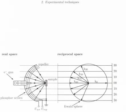
Low energy electron diffraction (LEED) is a m ethod for the study of atoms on sm-faces. It is one of th e principal techniques for the determ ination of the surface stru ctu re of solids [70]. Here, the interference of waves which leads to the formation of a diffraction p attern is being exploited. This diffraction p attern is then made visible on a screen. In detail, A conducting sample with a well-ordered crystalline surface structure is exposed to a monochromatic beam of low energy electrons ((w 20 200) eV) normal to the surface. According to the de Broglie relation
where A is the de Broglie wavelength, E the energy of the electron and nv its mass, this corresponds to wavelengths in the range of 0.5 A to 5 A. This range is of the same order of m agnitude as the lattice spacing of atom s in a crystal. The surface sensitivity of the measurement methods is due to the low penetration depth of the low energy electrons, which lies in the range of 0.5 nm to 1 nm. UHV conditions are crucial for the investigation of surfaces by LEED so th a t the sample surface remains free from im purities during the measurement. Furtherm ore, inelastic interactions of the diffracted electrons with gas molecules are avoided in a UHV environment.
2. Experim ental techniques
r e a l sp a c e r e c ip r o c a l s p a c e
repeller
e gun
sample
phosphor screen
Ewakl sphere r e p
30 20 10 00
lo
20 30 [image:26.536.41.483.47.438.2]2. E xp erim en ta l techniques
atom s can be considered to a c t as point scatterers. By th e principle of w ave-particle duality, th e beam of electrons m ay be equally regarded as a succession of electron waves incident norm al to the sam ple. A fter th e dispersion of th e electrons in th e sam ple, these are once m ore accelerated in th e direction of th e fluorescent screen. Before th e electrons hit th e screen th ey pass th ro u g h a num ber of energy-filtering grids on which an opposing field is applied. T his serves to filter out anj^ inelastically sc attere d electrons. T h e screen is illu m in ated a t th e positions of th e incom ing electrons, m aking th e diffraction p a tte rn visible. Ideally th is p a tte rn consists of bright sp o ts of light which are arran g ed sym m etrically. From th is sym m etry, th e sy m m etry of th e crystal surface can be calculated. In relation to scanning tu n n elin g m icroscopy it is pointed out th a t LEE D shows the reciprocal lattice. T his inform ation can also be o b tain ed from Fourier transform ed STM images. T hus, STM and LEE D m easurem ents can com plim ent each o th er a n d help to confirm th e m easured results.
In th e sim plest kinem atic exam ple, a diff’ractio n jm ttern is form ed analogous to th a t of a diffraction grating. O nly single sc atterin g from th e surface is considered in this exam ple. T his allows us to describe th e shape and size of th e surface unit cell, but it does n ot give inform ation a b o u t th e atom ic arran g em en t inside th e unit cell. C onsidering th e ato m s as point particles, th e incident plane wave will be scattered in all directions. For an ordered crystal surface, interference will restrict th e net flux to those directions where th e sc attere d waves are in phase. T his condition is m et only when th e scattered waves from neighbouring u n it cells differ by an integral num ber of w avelengths A. For th e sim ple case of a ID lattice, th is in-phase condition for constructive interference is illu stra te d in Fig. 2.4, w here th e incom ing beam is norm al to th e sam ple. Therefore, the positions a t which diffraction sp o ts occur is defined by th e B ragg equation.
nX = c?sin 6 (2.3)
2. Experim ental techniques
• • • •
% %
% \
\ \
Figure 2.1.: Schematic of the Bragg condition for a ID lattice. Only in the case of con structive interference between the scattered rays is it possible to detect a diffracted beam.
the screen giving an image of the reciprocal lattice of the surface. The real space lattice param eter li is related to the reciprocal space lattice param eter a* by a*=l/~a.
For surface diffraction to occur in a 2D system, with translational vectors h and
7
, the incoming electron beam nmst conserve both its energy and the component of its mom entum parallel to the surface:+ 5 = ^ + ^ ^ = ^ + (2.4)
where fcy and k± are the parallel and perpendicular mom entum components of the in cident beam, respectively; while k'\\ and k'± are those of the diffracted beam. The re ciprocal lattice vector, now labelled is related to the beam energy Ee^, the electron mass rrie, and the diffraction angle 9 by:
1^1 = \ha* + lb* \ — \ ~k\ ■ s in9 — ^ ^ ■ sin 6 (2-5)
h
[image:28.536.51.489.54.458.2]2. E x p e rim e n ta l techniques
are re la te d to th e real space ve cto r ~a, b and ~c by
^ 6 x ( f ( f x ' a ' ~a X b , ^
a — 2 tt——=f— — b = 2 t t ^ ——— — c = — — — =? (2.6) ~a ■ b x ' c b ■ ~c x~a ^ ■ ~a x b
U sing c o lu m n ve cto r re p re se n ta tio n o f (re cip ro ca l) p rim itiv e vectors, th e form ulae above can be re w ritte n using m a trix inversion:
r - 1
a*b*c* = 2 7 r [ a 6 c J (2.7)
In tw o dim ensions, these re la tio n s become [70]
a ^ ~ b - I f ^ 2 -k a - I f = ^ = 0 (2.8)
T h is shows th e d ire c t correspondence between th e observed d iffra c tio n p a tte rn and the re c ip ro c a l la ttic e o f th e surface. T h e re cip ro ca l la ttic e ve cto r g^i lies in a d ire c tio n th a t is o rth o g o n a l to th e plane o f the real space la ttic e w h ich is denoted by th e M ille r indices h and I. T h e M ille r indices o f th e d iffra c tin g planes are used to in d e x th e d iffra c tio n spots o f th e L E E D p a tte rn .
T h e d iffra c tio n p a tte rn can easily be described g ra p h ic a lly in reciprocal space by the c o n s tru c tio n o f the E w a ld sphere (F ig . 2.3). A sphere w ith rad iu s 1 /A is dra w n th ro u g h th e o rig in o f th e re cip ro ca l la ttic e . P^or each re cip ro ca l la ttic e p o in t th a t is located on th e E w a ld sphere o f re fle ctio n , th e B ragg c o n d itio n is satisfied and d iffra c tio n occurs.
2. Experim ental techniques
The observation of a LEED p attern does not guarantee th a t the whole surface is ordered. There is an instrum ental limit to the diam eter of the coherently scattering area on the surface called the coherence length. The significance is th a t interference will be strong within a coherent length of the source, but not beyond it. The coherence of an e-beam is limited by SB and the beam divergence. The spatial coherent length of a standard LEED optics is only (10 20)nm . Therefore, features and domains larger than the coherence length of the LEED optics will not result in a diffraction pattern.
Further information regarding crystal lattice structure may be obtained by both the position and the intensity of the spots. The position of the spots yields inform ation on the size, sym m etry and rotational alignment of the surface layers with respect to the synnnetry of the bulk crystal. The intensities of the various diffracted beams, which can be recorded as a function of the incident electron beam energy, generate so-called I-V curves. By comparison with theoretical curves, the I - V curves may provide accu rate information on atomic positions. While this is an extremely powerful technique, im fortunately we do not have the experim ental set-up to perform such measurements. Therefore, all of the LEED descriptions in this thesis are restricted to the simple kine matic approach.
2.3. Scanning tunneling microscopy
2. Exper iment al techniques
2.3.1. Theory of the tunneling effect
T h e principle behind th e o p eration of a STM is th e q u a n tu m tunneling effect. To un d e rsta n d this effect, consider an electron w ith energy E moving in a p o ten tial U(z). In classical m echanics, it is described by th e equation [71, 72]:
^ + U { z ) ^ E (2.9)
w here m is th e m ass of th e electron an d p its m om entum . In q u a n tu m m echanics, the s ta te of th e sam e electron is described by th e equation:
+ U{z)il;{z) ^ Eip{z) (2.10)
In th e classical case, it is possible to distinguish 2 situations: (/) T he allowed region, w here E > U{z) and th e electron has a nonzero m om entum p^ and (ii) th e forbidden region, w ith E < U { z ) which th e electron cannot p en etrate. In th e (juantm n m echanics case in th e region where E > U{z), equation 2.10 has solutions:
^ ( z ) = -0(0)6^'*''^ (2.11)
w here k is th e wave vector and is equal to k = ^j2rn{E — U) / h. In th e region where E < U{z) , i.e. th e tu nneling region, th e equation 2.10 has th e solution:
^ (2) = V '(0 )e “ '"‘ (2 .1 2 )
w here k is a decay co n stan t and is equal to: k = \ j 2 m { U — E) / h .
T he probability density of finding an electron near a point + z is p ro p ortional to 1^(0) which has a nonzero value in th e barrier region and thus a nonzero proba bility to p e n e tra te th e barrier. An analogous solution describes an electron s ta te in the
2. Experim ental techniques
This simple model explains some basic features of the one-dimensional metal-vacuum- nietal tunneling effect (a more detailed treatm ent can be found in [73]), shown in Fig.2.5. Now consider a metal surface and a sharp m etal tip placed within a few angstrom s of it.
(b) Sample ^T^!(77777777777777777777?
Sample
(c)
y777777777777y. '
V777777777777777V777777A
/^77 7 7 ^7 7 7 7 T / 0 Zq
Figure 2.5.: a) Tip (p r) and sani])le (ps) density of states with an applied bias voltage {eV). A bias voltage is necessary to have a net tunneling current It. Instead of solving the Schrodinger equation for the coupled tip-sample system, Bardeen used the approach of perturbation theory. By using two subsystems, b) and c), It is calculated through the overlap of t/) and x of the free systems using Fermi’s golden rule. [71]
[image:32.536.42.467.163.400.2]2. E xp e rim en ta l techniques
level, En « —(j). T h e p robability w to find an electron at th e tip surface 2 = VI', is given by:
w (X (2.13)
w here th e decay c o n stan t k is now given by k = \ / 2 m $ / h . T he sta te s on th e sam ple surface w ithin th e energy interval given by eV^ are responsible for the tunnel c u rren t If an d determ ine It as follows:
/to c ^ (2.14)
E n = E p —eVh
For small the sum in equation 2.14 can be w ritten using th e local density of sta te s (LDOS) a t th e Ferm i level. At a location 2. th e LDOS p s{z . E ) of th e sam ple is defined as p s { z , E ) = \'^n{z)\'^ for a sufficiently small e. T he value of the LDOS near th e Fermi level is an indicator of w h eth er th e surface is m etallic or not. T he It can be conveniently w ritte n in term s of the LD OS of the sample:
It<xVbPs{0,EF)e-'^^^^' (2.15)
T h e dependence of th e logarithm of It w ith respect to distance H ' is a m easure of the work function 0, or th e tunneling b a rrier height. It is also clear th a t th e It is very sensitive to sm all variations in the distance betw een tip an d sam ple.
2.3.2. The scanning tunneling microscope
2. Experim ental techniques
tunneling, proposed by Bardeen [74]. In this approach a transfer Hamiltonian H t is used to describe the tunneling of an electron, from a sample state 'ip, to a tip state x (see also Fig. 2.5. The tunnel current is a convolution of the sample LDOS ps and the tip LDOS
Pt
-/f = — / p s i E p - e V + E )p t{ Ef - E ) \ M \ ^ ( I E (2.16) n Jq
The tunneling current It also includes a tunneling m atrix element M , which describes the am plitude of electron transfer across the tum ieling barrier, as a function of the overlap between sample states
{ip)
and tip states(x)-It is determined by a surface integral over the medium separating th e two electrodes. If M is constant over the voltage range probed, the tunnel current is determ ined by a convolution of the LDOS of the two electrodes, the tip and the sample.
Once tunneling is established, the tip is scanned mechanically across the surface. There are two basic modes for the scanning process, namely, constant current or constant height. The most connnonly used mode is the constant current mode. In this case, the tunnehng cin'rent is kept constant in the range from a few pA to (1-2) nA, by a feedback control unit th a t changes the tip-sample separation in response to a change in the tunneling current. However, in the constant height mode, the barrier height is kept constant and the tunneling current recorded as a function of the tip position. In this thesis, the STM was operated in the constant current mode for all the measurements performed.
2.4. STM tips
2. E xp erim en ta l techniques
for tip p reparation. T ungsten is relatively h ard , m aking it a stable probe m aterial and it can be electrochem ically etched, allowing th e p rep aratio n of atom ically sh arp tip s [72].
M icropositioner
I
P T F E tu b in g
2 M NaO H
[
.rC' r,i • :
W rod
4 V dc bias
Stainless steal cathode
Figure 2.6.; E lectrochem ical etching set-u p used to prepare STM th e W -tips.
STM images in th is thesis were o b tain ed w ith W tips, which were prepared using a chem ical etching procedure described in detail elsewhere [75].
[image:35.536.24.488.105.814.2]2. E xp erim en ta l techniques
th e active etching region. T his leads to a stretch in g of th e wire a t th e interface region and eventually th e subm erged section of th e wire falls off u n d er its own weight.
D uring th e etching process, th e P T F E a c ts to physically restric t th e active region [76]
an d also pro tects th e tip th a t falls into th e beaker. T his tip etching set-up is shown in Fig. 2.6. T he tips are th en rinsed w ith propan-2-ol, placed in tip holders and inserted into UHV. T h e tips are th en etched w ith A r+ ions to remove th e W O^” present from th e chem ical etching process. T h is process produces stable, atom ically sh arp tips.
2. Experim ental techniques
2.5. X-ray absorption spectroscopy
X-ray absorption spectroscopy (XAS) is an umbrella term for several wiclely-usecl X-
ray spectroscopic measurement techniques: The near edge XAS (often abbreviated as
XANES for X-ray absorption near edge structure or NEXAFS for near edge X-ray ab
sorption fine structure) provides inform ation on vmoccupied electron states (orbitals)
for the chemical element under study and thus the chemical composition of the sample
to be tested. A sub-group is the near edge XAS with circularly polarised X-rays. This
technique uses X-ray dichroism and is used to study the m agnetisation of a sample.
If an X-ray photon enters a solid it can be absorbed and in this absorption process
a core electron is excited to an em pty state. If the energy of the X-ray photon is nuich
larger than the binding energy of the core state the excited electron behaves like a “free”
electron in the solid. However, if the X-ray energy is just enough to excite a core electron
it will occupy the lowest available em pty state. If the X-ray energy is too small to reach
an em pty state no excitation can occur.
CJ o
o
o
Incident photon energy
Figure 2.7.: Schematic view of X-ray absorption (left) and X-ray absorption coefficient as a function of incident photon energy (right).
XAS [77-79] measures the absorption of X-rays as a function of X-ray energy E — hi'.
The ratio of the X-ray intensity before and after interacting with the sample is measured
and the absorption determined. This transm ission measurement is the simplest method,
however, it requires th a t the sample is thin enough so th a t X-rays can pass through it.
sam-2. Experim ental techniques
pies would have to be extremely thin (in the range of a micrometer). For transm ission measurements both the bulk of the sample as well as its surface contribute to the ab sorption; however, the contribution of the surface is much weaker than th a t of the bulk, and therefore can not be determ ined separately. Fig. 2.7 (left) represents the schematic view of X-ray absorption in transmission. After the X-ray has traversed a distance x into the slab of absorbing m aterial, the intensity of the incoming X-ray beam Iq has been reduced to
I = Iq e x p { -i i x ), (2.18)
where // is the definition of the absorption coefficient. More specifically, the X-ray ab sorption coefficient //(£ ) = —d l n l / d x is determ ined from the decay in the X-ray beam
intensity I with distance x. If the absorption coefficient is plotted as a function of E (Fig. 2.7, right), the experim ental d ata show three general features: (i) an overall decrease in X-ray absorption with increasing energy; (ii) the presence of a sharp rise at certain en ergies called edges, which roughly resembles step-function increases in the absorption; and (iii) above the edges, a series of oscillatory stru cture th a t m odulate the absorption, typically by a few percent of the overall absorption cross section. The first feature is il lustrative of the well-understood quantum -m echanical phenomenon of X-ray absorption by atoms, as described, for example, by Ferm i’s Golden Rule (e.g., [80]). The energy position of the second feature is unique to a given absorption atom and reflects the ex citation energy of inner-shell electrons. The energy region close to the absorption edge (about 30 eV extension) is called XANES. Fig. 2.8 shows the transitions th a t contribute to the XAS edges and an example Fe 2p X-ray absorption spectrum .
E
n
e
rg
y
2. E xp erim en ta l techniques
T r a n s itio n s t h a t c o n t r ib u t e t o X A S e d g e s E x a m p le Fe 2p a b s o r p tio n s p e c tr u m
A bsorption
j M4 an d M5 edji;es M2 an d Ala edges ■ 4 - v - - - V - V - V = 3 p
____________3^
A bsorption
Li edge
2s
K edg( Is
2. E xperim ental techniques
yield, is therefore proportional to the number of electrons initially excited by the X-rays,
the total electron yield, and therefore a measure of the absorption coefficient. In this work
only the total electron yield was measured.
A nother possible process for the filling of an unoccupied state is the emission of an
X-ray photon (fluorescence photon). This process has in the soft X-ray regime a much
lower probability (typically in the tenth of a percent), as the Auger process. However,
since electrons are limited by their mean free path within a sample, fluorescence X-rays
can pass through a thicker layer than electrons. This way a larger part of the sample is
detected and the disadvantage of lower intensity partially compensated. The proportion
of the im mediate siu’face of the measuring signal is thus reduced, which is advantageous
if one is interested in the spectroscopy of the bulk of the sample and the contributions
2. E xperim ental techniques
2 .6 . X-ray m a g n e tic circular dichroism
X-ray magnetic circular dichroism (XMCD) is an innbrella term for a num ber of X-ray
spectroscopic effects based on the coupling of (X-ray) photons with specific electron
orbitals. The concepts of XMCD spectroscopy are presented in Fig. 2.9. In XMCD the
absorption of X-rays by an atom w ith a magnetic moment is dependent on w hether the
X-ray radiation is left or right circulary polarised. Relevant is the difference spectrum of
two XAS spectra taken in a magnetic field, one taken with left circularly polarised light,
and one with right circularly polarised light. When recording a polarised absorption
spectrum the direction of m agnetisation and the helicity of the X-ray photons is to be
aligned parallel and anti-parallel. The resulting absorption spectra are subtracted from
each other. From the difference, by applying the so-called “sum rules”, direct inform ation
about the element-specific spin moment and the spin-orl:)ital moment of the valence
band can be obtained. Typically XMCD studies magnetic transition metals such as iron,
cobalt, and nickel and their alloys or compounds. Recently, also metal complexes are
being studied by XMCD. In XMCD, XAS spectra arc measured at the 2p absorption
edge. Hereby transitions into the 3d shell occur, which may be strongly magnetic, lience
2. Experim entcil techniques
(a) c?-orbital occupation (b) Spin m om ent
t
V # < # .
(c) O rb ital m om ent
\ Holes
DOS
right
A
I = 2
I = 1
3. Density functional theory
In this thesis, density functional theory (DFT) calculations are employed to aid the
interpretation of experimental results. This chapter gives a short introduction to the
theoretical background of density functional and pseudopotential theory, as well as de
scribing details specific to the Vienna Ab-initio Simulation Package (VASP) used to
generate the results in this thesis [83]. For a more in-depth derivation and historical
background the reader is referred to the vast amount of literature which exists on these
topics. VASP is an ab-initio quantum-mechanical molecular dynamics (MD) software
package th a t uses pseudopotentials and a plane wave basis set to calculate an electronic
ground state. Although the description in this chapter is based on VASP, the concepts are
in general universal to all D FT codes [83, 84]. First the Born-Oppenheimer approxim a
tion and Bloch’s theorem are introduced. Then the basics of density functional theory
leading to the Kohn-Sham (KS) equations are described. The approxim ations for the
exchange-correlation (XC) energy th a t must be made in order to solve the KS equations
are discussed next. Pseudopotential theory is used as a way to minimise the number of
wavefunctions necessary to describe all the features of a valence electron moving through
a solid. In the final section, an introduction to molecular dynamics based on the calcu
lation of the Hellman-Feynman forces is given. Here, equations of motion are derived,
which determ ine the relaxation of the ions in the supercell towards a minimum energy
3. D ensity functional theory
3.1. Born-Oppenheimer approximation and Bloch’s theorem
It is necessary to know the particle density in order to study a system of interacting
electrons and nuclei. For this reason the construction of a suitable many-body wavefunc-
tion for the particular system is required. In principle, this wavefunction is a function of
tim e and all nuclear and electronic coordinates. However, a certain approxim ation can
be made to simplify the system.
Since nuclei are typically about 2000 times heavier th an electrons, the electronic and
nuclear motion can be decoupled by approxim ating th a t the electrons respond instan
taneously to any change in nuclear coordinates. This approxim ation then allows one to
rewrite the full many-body wavefunction as the product of a nuclear and an electronic
wavefunction. The electronic wavefunction can be described with the tim e-independent
Schrodinger equation. This can be done since it only depends on the instantaneous nu
clear configuration, and not on time. The nuclei are also massive enough to be treated
as classical particles. For th a t reason they respond to the electronic forces according to
Newtou's laws. T his seini-classical approxim ation, coupled w ith an adiabatic separation
of variables is called the Born-Oppenheim er approxim ation.
A further simplification can be made if studies are hm ited to periodic systems. Bloch’s
theorem states th a t any wavefmiction, of a periodic system must be the product of a
cell-periodic part U j(^) and a phase factor. This is in order to preserve the translational
■ ^
synunetry of the density. The phase factor takes the form of a plane wave, e , whose
wavevector is a linear com bination of reciprocal lattice vectors, and ^ { ' r ) is w ritten as:
with G ■ 7 = 27rm, m is an integer, are the crystal lattice vectors, are the
plane-wave coefficients, the subscript j indicates the band index and A; is a continuous (3.1) G
3. D e n s ity fu n ction al tlie o ry
sam e periodicity as th e direct la ttic e so th a t th e electron wavefiinctions can be expanded
in term s of a linear com bination of plane-waves:
Plane-w aves are a sim ple way of representing electron w avefunctions an d offer a com plete
equally. T his has th e a d d itio n al advantage th a t th e basis functions are orthogonal, and
t h a t o perations on th em are co m p u tatio n ally efficient. In p a rticu la r it is straightforw ard
to Fourier transform th e w avefunction from real space to reciprocal space or vice versa.
M any of th e system s under study, such as e. g. surfaces, are not periodic, and need
th e co n struction of a supercell. T his is essentially ju st a u nit cell, rep eated periodically
in space, b u t containing a “sp a ce r’' region to sep arate th e region of interest from its
periodic images.
Typically th e “sp acer” is a vacuum . T he advantage of B loch's theorem can be used
even for non-periodic system s by using supercells to represent th e system . Obviously, it
m ust be ensured th a t th is supercell is a good ap proxim ation of the original, aperiodic
system . T his is done by checking th a t th e results are invariant w ith respect to small
changes in th e size of th e supercell.
3.2. Hohenberg-Kohn theorem
T he H ohenberg-K ohn theorem s are th e foundations of D F T . T hey relate to any system
th a t consists of electrons m oving under th e influence of an ex ternal p o ten tial V e x t i ^ )
-T his functional is m inim ised for th e correct g ro u n d -state electron density. -T he ground-
s ta te energy functional is w ritte n as:
(3.2)
G
basis set. T he basis set is independent of th e ty p e of crystal and tre a ts all areas of space
3. Density functional theory
where Vext is the external potential, i. e. the potential related to the positions of the nuclei.
The main idea of the Hohenberg-Kohn theorem is th a t there is a one-to-one correspon
dence between the electron density ?i( r^) and the external potential. The functional F[n\
includes all electron-electron interaction and kinetic energy terms. It is convenient to
separately identify the energy due to the Coulomb interaction, also called the H artree
energy from F[n] :
f [ „ ] = ^ f [ + G[«| (3^4)
oTreo J J I r — r '
where e is the charge of the electron and eo is the electric perm ittivity of vacuum. Since
the cxact form of G[n] is unknown, the ground state of the system can be obtained by
minimising E[n\ with respect to the density while conserving N\
y n { 7 ) d r — N (3.5)
This leads to the variational equation:
S{ E[ n] —fi J n { ^ ) d l^ } — 0 (3-6)
A Lagrange nmltiplier, /z, is introduced due to the constraints of equation 3.5. By ap-
plyirig Eq. 3.3, Eq. 3.4 and Eq. 3.6 the ground state can be determ ined by:
f n(r') , , 5G[n]
Vex.ti'T ) + - / 1 y.dr -I- = /i (3.7) 47reo J \r — r'\ dn[ r )
where is the functional derivative of G[ri] with respect to n( r^). Even if the func
3. Density functional theory
3.3. Kohn-Sham (KS) equations
Kohn and Sham developed a m ethod resulting in one-particle equations, called the Kohn-
Sham (KS) equations, which may be solved [85]. The KS equations consider a system of
N non-interacting electrons in an external potential Vext,s{^)- The ground-state density
of this system is The functional F[n\ in Eq. 3.4 then reduces to T,[n], which is the
kinetic energy functional of non-interacting electrons. The equation determ ining n['r) is
then given by:
V e x t . s i ^ r ) + = M., (3.8)
on{ r )
In this case, the general form of Ts[n] is again unknown. However, there is a way to solve
it for For the case of non-interacting electrons, the many particle ground state
wavefunction is simply a product of single electron wavefunctions ^i(r^) th a t obey the
tim e-independent Schrodinger equation:
| - ^ V ^ + f e x t „ s ( ^ ) | <?^j(^) = t i ( t > i ( j ) A = 1...A'. (3.9)
where m denotes the electron mass. The density for this system of electrons is then given
by:
N
i=l
The ground state is found by selecting the N states, 0j( ?^), th a t have the lowest energy
e^. Moreover, there is a way of finding the solution to Eq. 3.8 for this particular system
of non-interacting electrons. This method is also valid for interacting electrons [85]. In
this case the functional G[n] may be split into two terms:
G[n] = Ts[n] + Exc[n] (3.11)
Here, th e first term is still the kinetic energy of a system of non-interacting electrons
3. D e n s ity fu n c tio n a l th e o ry
co n ta in s th e in fo rm a tio n o f th e in te ra c tin g system w ith d e n s ity n { 7 ) . E q u a tio n 3.7 now
becomes:
f n ( r ' ) , , 5Exc\n] STsln]
V e x t i r ) + --- / - ^ , d r ' + (3.12) 4vreo ./ \r — r \ d n ( r ) o n [ r )
T h is e q u a tio n has th e fo rm o f Eq. 3.8 except V e x t , s ( ^ ) is replaced by an effective p o te n tia l
V e f f [ n ] :
/-►V 9 C n ( r ' ) , , SEj-Jn]
V e f f [ n ] = V e x t i r ) + e 47reo / ^ - d r + ^ (3.13) j \r — r ' \ dn{ r )
A s w ith th e n o n -in te ra c tin g case, th e correct g ro u n d -sta te d e n sity o f th e in te ra c tin g
system is fo u n d by th e self-consistent s o lu tio n {Veff[n\ dependent on n { 7 ) ) o f th e single
p a rtic le K S equations:
f
1
+ V e f f { l ^ ) > 'i pi i ' r) = ^ I . . . N (3.14) 2m
X
i = l
T h e re fo re , the to ta l g ro u n d -sta te energy o f th e electron system is:
E [ n ] = T ,[n ] -1- j V e x t { ^ ) n { ' r ) d l ^ + j j ■ ” ’! » - -I- .E xcN (3.16)
W here:
Ts[n] = Z A { r ) d { 7 ) (3.17)
Some e x p lic it fo rm fo r Exc[»] n m st be ado p te d in o rd e r to fin d th e self-consistent
3. D ensity functional theory
Locally iinifonii electron gas
dr r
Figure 3.1.: Schematic diagram showing the principle of the local density approximation. For a given radial slab, dr, the local charge density is considered to be n{7) , the density of an equivalent uniform homogeneous electron gas.
3 .3 .1 . Local density approximation
The local density approxim ation (LDA) is the simplest approxim ation of the XC energy
functional which was first used by Kohn and Sham [85]. W ith the LDA. in regions of
space where the charge density is slowly varying, the XC energy can be considered as
a locally-uniform electron gas of the same charge density. The LDA functional assumes
th a t the per-electron XC energy at every point in space is eqTial to th a t of the per-electron
XC energy of a homogeneous electron gas. This can w ritten as
E x c = j d^rn{' r) (^37r^n( (3.18)
A schematic diagram showing the principle of the LDA is presented in Fig. 3.1
The LDA works very well despite its simplicity. It even works reasonably well in sys
tem s where the charge density is rapidly varying. However, it tends to imder-predict
atom ic ground state energies and ionisation energies, while over-predicting binding en
ergies. It is also known to greatly favour high spin state structures. For these reasons
3. Density functional theory
gradient corrections to incorporate longer range gradient effects [86]. However in prac
tice, althongli these improvements appear to result in b etter total energies, the resultant
structure is often worse, and at a greatly increased com putational cost. In general, the
LDA is worse for small molecules and improves with system size.
3 .3 .2 . Exchange-correlation
The only remaining problem is to find an approxim ate solution for the homogeneous
electron gas exchange correlation (XC) term , Sxc{n)- There are several param etrised
m ethods for this and the one used in VASP is based on the work by Ceperley and Alder
The correlation energy for a homogeneous electron gas comes from a set of quan
tum Monte Carlo calculations performed by Ceperley and Alder [87]. These were later
param etrised by Perdew and Zunger [88].
The results of Ceperley and Alder apply to low density electron gases, and can be
combined with results from perturbation theory for high density gases to cover a wide
density range. The m ethod defines the correlation energy per electron, Sc, polarisation
^ and Wigner-Seitz radius of each electron, ?■,, as: [87],
(3.19)
where n is the electron density. For the non-polarised = 0) and fully-polarised = 1)
cases, £c is given by [88]:
(3.20)
3. D e n s ity fu n ction al th e o ry
3.4. Pseudopotential theory
Given the fermionic nature of electrons, every electronic state of the system has to be
orthogonal to every other state. As higher and higher states are being filled, this means
the wavefunctions of these states have increasing numbers of nodes. This dram atically
increases the w idth of the Fourier spectrum , and hence the number of plane waves th a t
are needed to adequately represent the wavefunction.
Typically, the chemical properties of a molecule depend mainly on the valence elec
trons as opposed to the core electrons. Since core electrons occupy the inner, inert, shells
of atom s, their main function is to shield the outer valence electrons from the nuclei.
In the pseudopotential approxim ation, the electrons whose wavefunctions are localised
in the core region are removed. Their effective potential is combined with the nuclear
Coulomb potential and the resulting effective potential is called the pseudopotential.
Therefore, the remaining valence electrons' wavefunctions only have to be orthogonal
to each other, so the number of nodes is reduced. The pseudopotential is constructed
such th a t the wavefunctions outside the core region are vuichanged. The use of pseu
dopotentials dram atically reduces the mniiber of plane waves required to represent the
wavefunctions w ithout much effect on the results.
3.4.1. Projector Augmented-W ave Method
The electron wavefunctions of real m aterials have very different signatures in different
regions of space. In the bonding region, the wavefunction is fairly smooth, whereas
close to th e nucleus, due to the large attractive potential of the nucleus, it oscillates
rapidly. It is difficult for electronic structure m ethods to accurately describe the bonding
region whi


![Figure 2.5.: a) Tip (pr) and sani])le (ps) density of states with an applied bias voltage {eV)](https://thumb-us.123doks.com/thumbv2/123dok_us/1053003.621319/32.536.42.467.163.400/figure-tip-sani-density-states-applied-bias-voltage.webp)


