Abstract—This paper presents a simple configuration of a closed-loop switched-coupled-inductor inverter (SCII) by combining a non-overlapping phase generator and a sinusoidal pulse-width-modulation (SPWM) controller in order to realize boost DC-AC conversion and low-power regulation. The power part is composed of two sub-circuits between supply VS and
output VOUT, including: (i) a switched-copuled-inductor booster
(one coupled inductor, two pumping capacitors, and one switch regulated by the phase generator circuit), and (ii) a half-bridge DC-link inverter (one filter capacitor, a load resistor, and two switches controlled by the SPWM controller), so as to obtain the maximum range of AC output: +[(1+nD)/(1-D)]VS ~ -nVS,
where n is the turn ratio of the coupled inductor and D is duty cycle of charging this inductor. Practically, while D=0.42 and n=6, a symmetrical sinusoidal output: AC 100VRMS, 60Hz can
be obtained at the supply of DC 24V. Besdies, the SPWM is employed to enhance regulation capability for the different output amplitude and frequency, as well as robustness to source or loading variation. Finally, the closed-loop SCII is designed and simulated by SPICE for some cases of steady-state and dynamic responses. All results are illustrated to show the efficacy of the proposed scheme.
Index Terms—switched-coupled-inductor inverter, boost DC-AC conversion, cloased-loop regulation, sinusoidal pulse- width-modulation.
I. INTRODUCTION
ast several years, boost power converters for DC-DC or DC-AC are widely applied when a circuit or module has just a low-voltage source available, such as lighting device, smart phone, and medical equipment… etc. They are always required to be with some good characteristics, including small volume, light weight, high conversion efficiency, and robust regulation capability. Generally, the conventional converters have a larger volume and a heavier weight due to magnetic elements. Therefore, more manufactures and researchers pay attention to this topic, and ultimately aiming for DC-DC/ DC-AC step-up converters realized on a compact chip by mixed-mode VLSI technology.
This kind of switched-capacitor (SC) power converters, including only capacitors and MOSFET switches, is one of the good solutions to provide a high voltage gain for realizing the boost DC-DC/DC-AC conversion in the non-magnetic
Manuscript received December 1, 2017. This work is supported in part by Ministry of Science and Technology of Taiwan, R.O.C., under Grant MOST 106-2221-E-324-003. Yuen-Haw Chang, Kai-Lin Hsu, and Dian-Lin Ou are with the Department and Graduate Institute of Computer Science and Information Engineering, Chaoyang University of Technology, Taichung, Taiwan, R.O.C. Post code: 413. (e-mail address: [email protected],
[email protected], [email protected]).
circuit. Up to now, the various SC types have been suggested. In 1976, Dickson charge pumping was proposed based on a diode-capacitor chainstructure [1]. In 1990s, Ioinovici et al. proposed some SC schems with two capacitor cells working in anti-phase by voltage/current mode [2-3]. In 2007, Chang proposed a CPLD-based implementation of SC step-down DC-DC converter for multiple output choices [4]. In 2011-2013, Chang et al. proposed a series of multistage/ multiphase SC step-up/down DC-DC converter or DC-AC inverter [5-8]. In 2014, Chang et al. proposed a two-stage four-phase SC-based boost DC-AC inverter with sinusoidal PFM [9]. In 2015, Chang et al. proposed a closed-loop high-gain switched-capacitor-inductor-based boost DC-AC inverter [10].
For a higher voltage gain, it is one of the good ways to take advantage of turn ratio and/or extra winding stage of coupled inductor. But, the stress on transistors and the volume of magnetic device must be considered. In 2015, Chen et al. proposed a high-gain and input-current-ripple-free boost integrated flyback converter including coupled inductor [11]. Bahrami et al. suggested a modified step-up boost converter with coupled-inductor and super-lift techniques [12]. Chen et al. proposed a novel switched-coupled-inductor DC-DC step-up converter and its derivatives [13]. Wu et al. proposed a nonisolated high step-up DC-DC converter via adopting switched-capacitor cell [14]. Nouri et al. proposed an interleaved high-gain step-up DC-DC converter based on three-winding coupled-inductor and voltage-multiplier cell [15]. In 2016-2017, Chang et al. proposed a novel coupled- inductor switched-capacitor boost DC-AC inverter, and then plus a four-stage SC, presented a high-gain serial-parallel- switched-capacitor coupled-inductor inverter [16-17]. Here, under the consideration of circuit complexity reduction, the authors attempt to propose a simple SCII scheme for boost DC-AC conversion and closed-loop regulation.
II. CONFIGURATION OF SCII
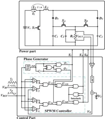
Fig. 1 shows the simple closed-loop switched-coupled- inductor inverter (SCII) proposed, and it contains two major parts: power and control part for achieving the boost DC-AC conversion and closed-loop regulation. These two parts are discussed as follows.
A. Power Part
The power part of this inverter as in the upper half of Fig. 1 contains two sub-circuits: (i) a switched-coupled-inductor booster and (ii) a half-bridge DC-link inverter, which are in
A Simple Switched-Coupled-Inductor
Inverter for Boost DC-AC Conversion and
Closed-Loop Regulation
Yuen-Haw Chang, Kai-Lin Hsu, and Dian-Lin Ou
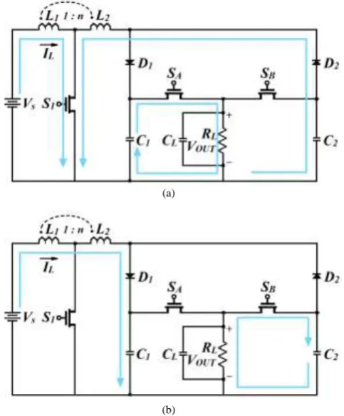
cascaded connection between supply VS and output VOUT . Firstly, the front-stage booster circuit is mainly in charge of step-up DC-DC conversion, including a MOSFET switch S1, a coupled inductor L1, L2, diodes D1-D2, pumping capacitors C1, C2, where the same capacitance C (C1=C2=C) is assumed. This coupled inductor (L1 and L2) is modeled as an ideal transformer with a turn ratio of n (n=N2/N1). The main function of this front stage is to lift the values of voltage across C1, C2 up to [(1+nD)/(1-D)]VS and nVS respectively, where D (0<D<1) is the duty cycle and DTS is the period of charging this coupled inductor in one switching cycle TS (TS=1/fS, fS: switching frequency). Secondly, the rear-stage circuit: half-bridge DC-link is to handle DC-AC invertsion. It includes two switches SA, SB of SWPM control, a filter capacitor CL, and a load resistor RL, and additionally half- bridge pumping capacitors C1, C2. With the help of SA and SB in the half-bridge, the maximum range of the AC output VOUT can reach to: +[(1+nD)/(1-D)]VS ~-nVS. Fig. 2 shows the theoretical waveforms within an output cycle TO (TO=1/fO, fO: output frequency). Here, for the convenience of explanation, one TO contains 11 (or above actually) switching cycle TS. Each TS has two phases: Phases I and II with the different periods DTS and (1-D)TS. The detailed operations are discussed as follows.
1) Phase I:
During this time interval, turn ON S1, turn SPWM-ON SA, and turn OFF SB. Then, diode D2 is turned ON, and D1 is turned OFF. The relevant topology is shown in Fig. 3(a). The inductor L1 is charged by supply VS, and the energy is transferred from the primary winding of this coupled inductor to the secondary one for making the voltage as: VL1=VS, VL2=nVS. And then, the energy stored in the secondary winding is transferred into C2 via S1 and D2 for making capacitor voltage VC2 towards -nVS. At the same time, the siagnal from SPWM controller can control switch SA ON or not, so as to make C1 discharging the energy into CL and RL, and then VOUT is heading towards the direction of the positive output.
2) Phase II:
[image:2.595.115.472.57.460.2]During this time interval, turn OFF S1 and SA, and turn SPWM-ON SB. Then, diode D1 is turned ON, and D2 is turned OFF. The relevant topology is shown in Fig. 3(b). According to the theory of the booster, the steady-state voltage VL1 across L1 is going towards the value of -DVS/(1-D) via the operation of duty cycle D, and thus the voltage VL2 across L2 in the secondary side is approaching the value of -nDVS/ (1-D). Then, C1 is
Fig. 2. Theoretical waveforms of closed-loop SCII.
charged by VS, VL1, VL2 in series via D1 (VS+|VL1|+|VL2| →VC1), and so VC1 is charged towards VS +DVS/(1-D)+ nDVS/(1-D)= +[(1+nD)/(1-D)]VS. At the same time, the siagnal from SPWM controller can control switch SB ON or not, so as to make C2 discharging the energy into
(a)
[image:3.595.308.550.53.345.2](b)
Fig. 3. Topologies for Phase (a) I and SA: SPWM-ON,
(b) II and SB: SPWM-ON.
CL and RL, and then VOUT is heading towards the direction of the negative output.
Based on the cyclical operations of Phase I and II, the overall step-up output VOUT can reach to the AC output range as: +[(1+nD)/(1-D)]VS ~-nVS. Here, the voltage gain is at about 5.89 (supply DC 24V, output AC 100V, 60Hz, AC peak: 142V), and so turn ratio n is taken by the nearest integer 6. For the symmetry of positive and negative output, let (1+nD)/(1-D) equal to n, and then the duty cycle D can be obtained at about 0.42. Thus, by using D=0.42 and n=6, it is reasonable that a symmetrical sinusoidal output can be attained from DC 24V to AC 100VRMS, 60Hz.
B. Control Part
U2, U3 and U4), and following by using logic-AND to produce a set of control signals U12, U34 for realizing SPWM. When e>0 and |e| is raising (e=VREF -VO), the pulse width of U12 is getting bigger. When e<0 and |e| is raising, the pulse width of U34 is getting bigger. And then, via the interlock circuit (avoid SA and SB being 1 simultaneously) plus coming into the phase of Φ2, SA and SB can be obtained for the SPWM control. The main goal is to keep VO on following VREF (sinusoidal reference) to enhance the regulation capability of this proposed inverter. To summarize, based on VO and VREF, the relevant rules of producing the control/driver signals are listed as below.
1) Φ1, Φ2: non-overlapping antiphase signals;
S1=Φ1.
2) If VREF > VRP, then U1=1;
If VREF < VRP, then U1=0.
If VRP > VO, then U2=1;
If VRP < VO, then U2=0.
If VO > VRP, then U3=1;
If VO < VRP, then U3=0.
If VRP> VREF, then U4=1;
If VRP< VREF, then U4=0.
3) If U1=1 and U2=1, then U12=1;
If not, then U12=0.
If U3=1 and U4=1, then U34=1;
If not, then U34=0.
4) If U12=1 and Φ2=1, then U12S=1;
If not, then U12S=0.
If U34=1 and Φ2=1, then U34S=1;
If not, then U34S=0.
5) SPWM control signals: (^: logic-AND)
SA= U12S, for VREF >VO.
SB= U34S, for VREF <VO.
(Interlock : SA ^SB ≠ 1)
III. EXAMPLES OF SCII
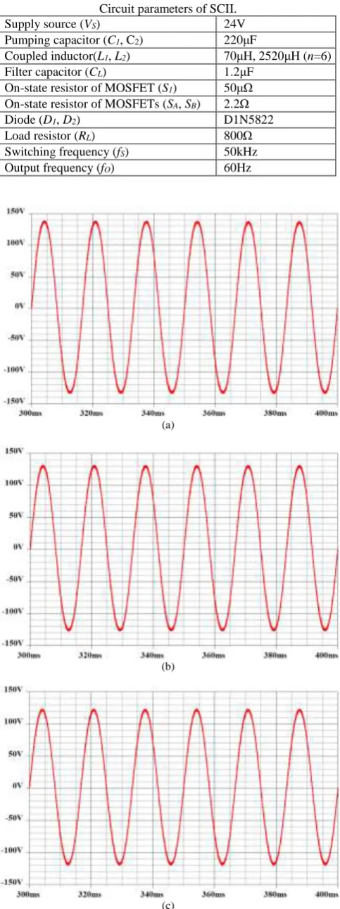
In this paper, the proposed SCII is simulated by SPICE, and all the parameters are listed in TABLE I. Based on these parameters, we have three cases for steady-state responses and four cases for dynamic responses in total. Then, these results are illustrated to verify the efficacy of the proposed inverter.
1) Steady-State Responses:
Case 1: fO=60 Hz, Vm=145V
Let the supply source VS be DC 24V, load RL be 800Ω, and the peak value and output frequency of VREF are Vm=145V, fO=60Hz. The waveform of VOUT is obtained as in Fig. 4(a). VOUT has the
TABLEI Circuit parameters of SCII.
Supply source (VS) 24V
Pumping capacitor (C1, C2) 220μF
Coupled inductor(L1, L2) 70μH, 2520μH (n=6)
Filter capacitor (CL) 1.2μF
On-state resistor of MOSFET (S1) 50μΩ On-state resistor of MOSFETs (SA, SB) 2.2Ω
Diode (D1, D2) D1N5822
Load resistor (RL) 800Ω
Switching frequency (fS) 50kHz
Output frequency (fO) 60Hz
(a)
(b)
(c)
Fig. 4. Output VOUT for VREF: (a) fO =60Hz, Vm =145V; (b) fO=60Hz,
Vm=135V; (c) fO =60Hz, Vm=125V.
practical peak value of 140V (i.e. 99VRMS), and the
[image:4.595.307.549.60.707.2]Case 2: fO=60 Hz, Vm=135V
Let the supply source VS be DC 24V, load RL be 800Ω, and the peak value and output frequency of VREF are Vm=135V, fO=60Hz. The waveform of VOUT is obtained as in Fig. 4(b). VOUT has the practical peak value of 131V (i.e. 92.6VRMS), and
the practical output frequency is about 60Hz. The efficiency is 66.7% and THD is 1.449%.
Case 3: fO=60 Hz, Vm=125V
Let the supply source VS be DC 24V, load RL be 800Ω, and the peak value and output frequency of VREF are Vm=125V, fO=60Hz. The waveform of VOUT is obtained as in Fig. 4(c). VOUT has the practical peak value of 123V (i.e. 86.9VRMS), and
the practical output frequency is about 60Hz. The efficiency is 61.2% and THD is 1.161%.
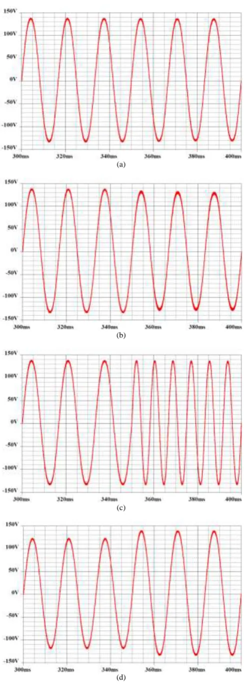
2) Dynamic Responses:
Since the voltage of battery is getting low as the battery is working long time, or the bad quality of battery results in the impurity of supply voltage, such a variation of supply voltage VS must be considered, as well as variation of load RL and/or sinusoidal reference VREF (fO or Vm).
Case 1: VS variation
Assume that VS is normally at DC 24V, and then it has an instant voltage drop: 24V→23V on 350ms (VREF: fO=60Hz, Vm=145V). The waveform of VOUT is shown as in Fig. 5(a). Obviously, VOUT has a slight decrease into about 138V.
Case 2: RL variation
Assume that RL is 800Ω normally, and suddenly it changes from 800Ω to 400Ω on 350ms (VREF: fO= 60Hz, Vm=145V). Fig. 5(b) shows the transient waveform of VOUT at the moment of loading variation. Obviously, VOUT has a small drop but can still be following VREF.
Case 3: fO variation
Assume that the frequency fO of VREF is 60Hz normally. After a period of 350ms, and it suddenly changes from 60Hz to 120Hz. Fig. 5(c) shows the transient waveform of VOUT at the moment of variation as VREF: fO=60Hz→120Hz, Vm=145V. Obviously, VOUT is still able to follow VREF even the frequency of VREF changes.
Case 4: Vm variation
Assume that Vm is 125V normally, After a period of 350ms, and it changes from 125V to 145V. Fig. 5(d) shows the transient waveform of VOUT at the moment of variation as VREF: fO=60Hz, Vm=125V →145V. Obviously, VOUT is still able to follow VREF even the amplitude of VREF changes.
According to the above results, it is obvious that VOUT is following VREF for the cases, including VS source variation, RL loading variation, fO frequency variation, Vm amplitude
(a)
(b)
(c)
[image:5.595.305.550.44.730.2](d)
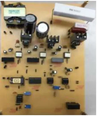
Fig. 6. Prototype circuit of closed-loop SCII.
IV. CONCLUSIONS
This papae presnts a simple SCII scheme with combining a phase generator and a SPWM controller for boost DC-AC conversion and closed-loop regulation. The power part is composed of a switched-copuled-inductor booster and a half-bridge DC-link inverter between VS and VOUT, so as to obtain the boost output range: +[(1+nD)/(1-D)]VS ~-nVS, where n is the turn ratio of the coupled inductor and D is duty cycle of charging this inductor. Practically, while D=0.42 and n=6, a symmetrical sinusoidal output: AC 100VRMS, 60Hz
can be obtained at the supply of DC 24V. Finally, the closed-loop SCII is designed and simulated by SPICE for some cases: steady-state and dynamic responses. The advantages of the proposed scheme are listed as follows. (i) This SCII needs just one coupled-inductor device. Except this, other components (including switches, diodes, and capacitors) can be made in IC fabrication promisingly. (ii) This proposed inverter sure is to present a simple configuration for boost DC-AC conversion via using fewer component count here. It is beneficial to circuit complexity decrease as well as coat reduction. (iii) For a higher gain, it can be realized with increasing the turn ratio of coupled inductor or extending the number of pumping capacitors. (iv) The SPWM technique is adopted not only to enhance output regulation capability for the different desired output, but also to reinforce the output robustness against source and loading variation. At present, the prototype circuit of this inverter is implemented in the laboratory as in the photo of Fig. 6. Some experimental results will be obtained and measured for the verification of the proposed inverter.
REFERENCES
[1] John F. Dickson, “On-chip high-voltage generation in MNOS integrated circuits using an improved voltage multiplier technique,”
IEEE Journal of Solid-State Circuits, vol. 11, no. 3, pp. 374-378, Jun. 1976.
[2] On-Cheong Mak, Yue-Chung Wong and Adrian Ioinovici, “Step-up DC power supply based on a switched-capacitor circuit,” IEEE Transactions on Industrial Electronics, vol. 42, no. 1, pp. 90-97, Feb. 1995.
[3] Guangyong Zhu and Adrian Ioinovici, “Steady-state characteristics of
switched-capacitor electronic converters,” Journal of Circuits, Systems and Computers, vol. 7 , no. 2, pp. 69-91, 1997.
[4] Yuen-Haw Chang, “CPLD-based closed-loop implementation of switched-capacitor step-down DC-DC converter for multiple output choices,” IET Electric Power Applications, vol. 1, issue 6, pp. 926-935, Nov. 2007.
[5] Yuen-Haw Chang, “Design and analysis of multistage multiphase switched-capacitor boost DC-AC inverter,” IEEE Transactions on Circuitsand Systems I: Regular paper,vol. 58, no. 1, pp. 205-218, Jan. 2011.
[6] Yuen-Haw Chang, “Variable-conversion-ratio multistage switched- capacitor-voltage-multiplier/divider DC-DC converter,” IEEETrans. on Circuits and Systems I: Regular paper, vol. 58, no. 8, pp. 1944-1957, Aug. 2011.
[7] Yuen-Haw Changand Ming-Zong Wu, “Generalized mc x nc -stage switched-capacitor-voltage-multiplier-based boost DC-AC inverter,”
International Journal of Electronics, vol. 99, no. 1, pp. 29-53, Jan. 2012.
[8] Yuen-Haw Chang and Yun-Jie Huang, “Closed-loop 7-Level switched-capacitor boost DC-AC inverter with sinusoidal PFM control,” International MultiConference of Engineers and Computer Scientists 2013 (IMECS'2013),vol. 2, Hong Kong,pp. 641-646, March 13-15, 2013.
[9] Yuen-Haw Chang, Chin-Ling Chen and Po-Chien Lo, “2-Stage 4-Phase Switched-Capacitor Boost DC-AC Inverter with Sinusoidal PFM Control,” International MultiConference of Engineers and Computer Scientists 2014 (IMECS'2014), vol. 2, Hong Kong, pp. 673-678, March 12-14, 2014.
[10] Yuen-Haw Chang, Yu-Kai Lin, “A closed-loop high-gain switched- capacitor-inductor-based boost DC-AC inverter,” International MultiConference of Engineers and Computer Scientists 2015 (IMECS'2015), vol. 2, Hong Kong, pp. 694-699, March 18-20, 2015. [11] Zhangyong Chen, Qun Zhou and Jianping Xu, “Coupled-inductor
boost integrated flyback converter with high-voltage gain and ripple- free input current,”IET power Electronics, vol. 8, pp. 213-220, Feb. 2015.
[12] Hamid Bahrami, Hossein Iman-Eini, Babak Kazemi, Alireza Taheri, “Modified step-up boost converter with coupled-inductor and super-lift techniques,”IET power Electronics, vol. 8, pp. 898-905, Jun. 2015. [13] Shih-Ming Chen, Man-Long Lao, Yi-Hsun Hsieh, Tsorng-Juu Liang,
Kai-Hui Chen, “A novel switched-coupled-inductor DC-DC step-up converter and its derivatives,” IEEE Transactions on Industry Applications, vol. 51, no. 1, pp. 309-314, Jan. 2015.
[14] Gang Wu, Xinbo Ruan, Zhihong Ye, “Nonisolated high step-up DC-DC converters adopting switched-capacitor cell,” IEEE Transactions on Industrial Electronics, vol. 32, no. 1, pp. 383-393, Jan. 2015.
[15] Tohid Nouri, Seyed Hossein Hosseini, Ebrahim Babaei and Jaber Ebrahimi, “Interleaved high step-up DC-DC converter based on three-winding high-frequency coupled inductor and voltage multiplier cell,” IET Power Electronics, vol. 8, no. 2, pp. 175-189, Feb. 2015. [16] Yuen-Haw Chang, Jyun-Jia Liao, “A novel coupled-inductor switched-
capacitor inverter for high-gain boost DC-AC conversion,”
International MultiConference of Engineers and Computer Scientists 2016 (IMECS'2016), vol. 2, Hong Kong, pp. 603-608, March 16-18, 2016.
[17] Yuen-Haw Chang and Zheng-Bin Li, “A high-gain serial-parallel- switched-capacitor coupled-inductor boost DC-AC inverter,”