_____________________________________________________________________________________________________
*Corresponding author: Email: [email protected], [email protected];
A Study of Wafer Backgrinding Tape Selection for
SOI Wafers
Bryan Christian S. Bacquian
1and Frederick Ray I. Gomez
1*1STMicroelectronics, Inc., Calamba City, 4027, Laguna, Philippines.
Authors’ contributions
This work was carried out in collaboration between both authors. Both authors read, reviewed, and approved the final manuscript.
Article Information
DOI: 10.9734/JERR/2019/v6i216943
Editor(s):
(1) Dr. P. Elangovan, Associate Professor, Department of EEE, Sreenivasa Institute of Technology and Management Studies, Chittoor, Andhra Pradesh, India.
Reviewers:
(1)A. Ayeshamariam, Khadir Mohideen College, India. (2)Snehadri Ota, Institute of Physics, India. (3)Xingming Long, Chongqing Normal University, China. Complete Peer review History:http://www.sdiarticle3.com/review-history/50004
Received 25 April 2019 Accepted 06 July 2019 Published 11 July 2019
ABSTRACT
The continuous development and trends on thinner semiconductor packages have become the focus in the semiconductor industry. The necessity of thinner packages also demands a thinner vertical structure of the integrated circuit (IC) design. As a major contributor on the vertical structure of the IC package, die or wafer is also essential to go thinner. As the wafer goes thinner, various problems may occur during transport and even the backgrinding process, itself.
Wafer warpage is one of the main concerns during the backgrinding process. Wafer warpage varies depending on the wafer backgrinding stress and backgrinding tape (hereinafter referred to as BG tape) tension. Hence, tension between the surface protective tape and the wafer should be considered an important and critical item to consider during BG tape selection.
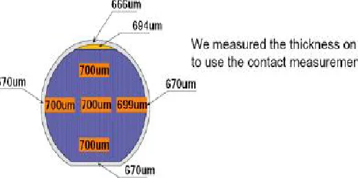
Different silicon wafer technology has been released to cater different functionality on different industry markets. One popular silicon technology is Silicon On Insulator (SOI) technology. SOI wafers have a step type passivation wherein the edge of the wafer is observed to have 30um thinner than its center. The stepping effect also contributes to the 0.5mm wafer warpage prior backgrinding. Evaluating the effect of BG tape selection to eliminate such warpage is discussed on this paper.
Bacquian and Gomez; JERR, 6(2): 1-6, 2019; Article no.JERR.50004
Keywords: Silicon on insulator; backgrinding tape; wafer preparation; SOI wafer.
1. INTRODUCTION
Achieving the package requirements of an integrated circuit (IC) semiconductor device would mean attaining a thinner die during the back end process. The major process brick responsible for grinding the silicon die to its thickness is wafer backgrinding. As a major preliminary process at the back end, one of its sub-processes is the wafer preparation prior grinding wherein silicon wafer is been taped on the active layer to protect it from any contaminants and water penetration during the grinding process.
One major factor for wafer warpage after grinding is the wafer backgrinding tape (hereinafter referred to as BG tape). The adhesion strength of the BG tape will induce the amount of wafer warpage and edge chipping of the grinded wafer. The study focuses on the effect of different BG tapes that can handle wafer warpage.
1.1 Silicon on Insulator Wafer
Silicon on insulator (SOI) wafer technology refers to the use of a layered silicon-insulator-silicon substrate, to reduce parasitic capacitance and thereby improving performance [1-2]. The implementation of SOI technology is one of several manufacturing strategies employed to
allow the continued miniaturization of
microelectronics colloquially referred to as extending Moore's Law [2-3]. SOI process has been developed so as to be used for RF applications [4]. The inclusion of enhanced sapphire substrate allows the complementary metal-oxide semiconductor (CMOS) node to
have a high isolation, high linearity, and electrostatic discharge (ESD) tolerance. The glass passivation on the wafer’s top layer creates a stepping effect on the edge of the wafer in Fig. 1.
Fig. 1. Wafer edge structure
In line with the stepping effect, SOI wafers are measured prior wafer taping and observed to have the edge area 30µm thinner than the device area as depicted in Fig. 2. Also, the wafers after having taped are observed to have a warpage in Fig. 3 of 0.5mm around the edge area.
1.2 Wafer Backgrinding Tape
Wafer BG tape is the main protector of the wafer on the stresses present during mechanical grinding. Aside from protecting the active circuit of wafer, BG tape would also help eliminate water penetration, breakage or cushioning adsorb during grinding process and maintain uniformity after grind, which have been verified by total thickness variation (TTV). BG tape adhesion strength should be carefully evaluated
otherwise wafer breakage or adhesive
contamination will be encountered. BG tapes are classified according to its adhesive material; the two types of BG tape are: Conventional non-ultraviolet (non-UV) type and UV curable type.
Fig. 3. Wafer warpage after taping
Due to inherent wafer warpage of the SOI wafers, the two different types have been used to check if it helps adsorb the grinding stress and prevent wafer breakage during grinding/detaping process. Both BG tape have almost the same tape thickness of 124-125 µm, but different on the adhesive material used.
2. LITERATURE REVIEW
2.1 Wafer Warpage Mechanism
A common wafer mechanism is a normal warpage [5] depicted in Fig. 4. This is generally caused by the natural stress created by
mechanical backgrinding. The proportional
relationship of wafer warpage and mechanical stress states that when the final thickness
decrease this probably caused by high
mechanical stress that may lead to high wafer
warpage. Although subsequent assembly
processes contribute to warpage, these
processes also adapt with the development and trend on wafer technology [6-7].
2.2 Mechanical Stress after Wafer
Backgrinding
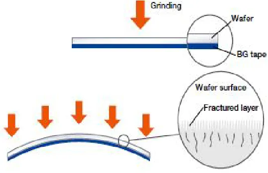
Stresses applied during encapsulation may crack the die and cause other stress-related failures. Optimized wafer strength is needed to ensure reliability during both fabrication and packaging. However, grinding anything inevitably leaves flaws on its surface, which can weaken both the wafer and the individual dice sawn from it. Given thermal or mechanical stress, these flaws may then spread into active regions, and may crack the die.
Bacquian and Gomez; JERR, 6(2): 1-6, 2019; Article no.JERR.50004
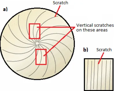
Fig. 5. Vertical scratches after wafer backgrinding
After backgrinding, the wafer will exhibit a scratch pattern on the backside as shown in Fig. 5. These scratch patterns and the depth of the scratches on the surface of the wafer are directly proportional to the size of the grit and the pressure exerted on the wafer during the grinding process. The depth of the scratches and the backside surface roughness of the semi-conductor die have a direct correlation to the strength of the die, so it is critical that the finished backside surface of the wafer be as smooth (or polished) as possible [8].
3. EXPERIMENTATION
3.1 BG Tape Selection
One major factor that could help minimize the wafer warpage is the BG tape. Proper selection of the BG tape involves the study of the adhesion strength of the tape towards the wafer during wafer back grinding thus inducing a much more wafer warpage after backgrinding.
Two different BG tapes in Table 1 have been evaluated to help reduce the wafer warpage prior and after wafer back grinding. Both tapes are on almost the same thickness, 125µm and 120µm respectively. Conventional tape is observed to have lowered adhesion strength before UV compare to UV tape BG tapes. However, UV types improves to 0.1N/25mm after UV exposure
that could possibly help lessen the stress of the BG tape during the detaping issue thus reducing wafer warpage. Wafer warpage and wafer edge chipping will depend on the effectiveness of the BG tape.
4. RESULTS AND DISCUSSION
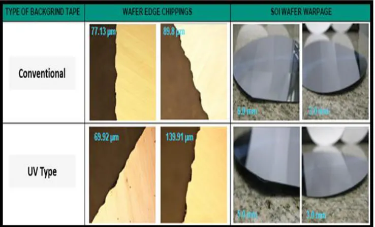
Both BG tapes in Fig. 6 induced wafer edge chippings and wafer warpage. The amount of wafer warpage for both BG tapes shows comparable level after backgrinding. Wafer edge chippings are observed being similar for both BG tapes. The readings of both tapes showed potential cause of wafer breakage. Both BG tapes have not been successful to be processed using the full auto mode due to its high warpage during the unloading. The robot arm vacuum is not enough to handle even the minimum warpage of 3.0mm.
Back side image of the wafer has also been inspected using high magnification microscope as shown in Fig. 7. Uneven surface was observed at the edge of the wafer, which can also be considered a potential cause of broken wafer during process of transporting wafer from one station to another at pre-assembly. Also, the occurrence of uneven surface at the back of the wafer also coincide with the step at the edge of the wafers.
Table 1. BG tape configuration
Specification Unit Conventional UV tape
Total thickness µm 125 120
Adhesive thickness µm 20 40
Adhesion strength Before UV N/25mm 2.84 6.5
Fig. 6. Wafer edge chipping and wafer warpage after backgrinding
Fig. 7. Back side image of the SOI wafer
Table 2. Quality index
BG tape broken wafer wafer edge chippings wafer warpage risk level
Conventional Medium High Medium High
UV Type Medium High Medium High
Table 2 summarizes the risk level of the evaluated BG tape configuration, having no significant effect across all critical wafer backgrinding responses, namely broken wafer,
Bacquian and Gomez; JERR, 6(2): 1-6, 2019; Article no.JERR.50004
5. CONCLUSION AND RECOMMENDA-TIONS
Adhesion strength of the BG tape was negated by normal warpage phenomena on the wafer. The BG tape, even on UV type tapes, could not equalize the amount of mechanical stress on the wafer surface structure thus increasing the effect of wafer warpage towards the silicon wafer. Both BG tape also could not negate the step type structure of the wafer thus creating wafer edge chippings and could be resulting wafer warpage if not fully controlled during handling.
For future works, detailed mathematical model and measurement indexes should be considered and qualified. For further improvement, it is highly recommended to use high vacuum efficient chuck table to properly handle incoming wafer warpage and ensure good flattening on the chuck table and eliminating the possibility of inferior grinding. Redesign of special robot arms should also be considered to eliminate the possibility of wafer breakage when handling or unloading thinner wafers after grinding or use an inline BG-mount system. Moreover, a special process should be considered wherein making an outer circumference lip, where no grinding pressure is applied on the edge of the wafer
during backgrinding. For ensuing critical
processes like that of the wafer saw, discussions in [9] are helpful to prevent or eliminate defects related to wafer preparation. Also, it is highly important that the assembly manufacturing processes ensure appropriate ESD checks and controls. Discussions quoted in [10] are very helpful to comprehend ESD-related controls.
ACKNOWLEDGMENTS
The authors would like to share appreciation and gratitude to the Central Engineering and Development – New Product Introduction (NPI) team and colleagues of STMicroelectronics Calamba who have greatly contributed to the success of the work. The authors are thankful to the Management Team for the extended support.
COMPETING INTERESTS
Authors have declared that no competing interests exist.
REFERENCES
1. Celler GK, Cristoloveanu S. Frontiers of
silicon-on-insulator; 2003.
2. Wosinski L, Wang Z, Tang Y. Interfacing of
silicon-on-insulator nanophotonic circuits to the real world. 12th International
Conference on Transparent Optical
Networks; 2010.
3. Mendez H. Silicon-on-insulator - SOI
technology and ecosystem - Emerging SOI applications; 2009.
4. Chen CL, Chen CK, Yost DR, Knecht JM,
Wyatt, PW, Burns JA, Warner K, Gouker PM, Healey P, Wheeler B, Keast CL. Wafer-scale 3D integration of silicon-on-insulator RF amplifiers. IEEE Topical Meeting on Silicon Monolithic Integrated Circuits in RF Systems; 2009.
5. “Wafer Breakage Due to Backgrinding”,
The Cutting Edge Technical Newsletter; 2008.
6. Doering R, Nishi Y. Handbook of
semi-conductor manufacturing technology. 2nd ed., CRC Press, USA; 2007.
7. Geng H. Semiconductor manufacturing
handbook. 1st ed., McGraw-Hill Education, USA; 2005.
8. Combs E. The back-end process: Step 3 -
Wafer backgrinding; 2002.
9. Sumagpang A, Gomez FR. Line stressing
critical processes optimization of scalable package passive device for successful
production ramp-up. Journal of
Engineering Research and Reports. 2018; 3(1):1-13.
10. Gomez FR. Improvement on leakage
current performance of semiconductor IC packages by eliminating ESD events.
Asian Journal of Engineering and
Technology. 2018;6(5).
© 2019 Bacquian and Gomez; This is an Open Access article distributed under the terms of the Creative Commons Attribution License (http://creativecommons.org/licenses/by/4.0), which permits unrestricted use, distribution, and reproduction in any medium, provided the original work is properly cited.
Peer-review history: