Available Online At www.ijpret.com
INTERNATIONAL JOURNAL OF PURE AND
APPLIED RESEARCH IN ENGINEERING AND
TECHNOLOGY
A PATH FOR HORIZING YOUR INNOVATIVE WORK
EFFICIENT DESIGN OF CMOS CIRCUITS USING NEW REVERSE BODY BIASED
TECHNIQUE IN DOMINO LOGIC FOR SUB THRESHOLD LEAKAGE REDUCTION
ANJANA R1, Dr. AJAY KUMAR SOMKUWAR2
1. Laxmi Institute of Technology, Electronics and communication, Sarigam, Gujarat.
2. MANIT, Electronics and communication Bhopal(MP).
Accepted Date:
03/10/2012
Publish Date: 12/10/2012
Keywords
Conventional body bias
RBB
Dynamic Logic
Deep Sub Micron
Full swing
Corresponding Author
Mrs. ANJANA R
Laxmi Institute of
Technology, Electronics
and communication,
Sarigam, Gujarat
Abstract
Domino logics are widely used in modern VLSI circuits for its
high speed over the static CMOS circuits. But the main
drawback of this domino logic is more susceptible to noise
and increased power dissipation. A Dynamic logic which
combines the advance of high speed and noise tolerant
circuit is used in recent CMOS VLSI circuits. In this paper, we
propose several domino logic circuit techniques to improve
the robustness and performance along with leakage power
using the new novel reverse body biased (RBB) technique. In
this work, different types of AND gates with Conventional
Body Bias & reverse body bias inverters are compared with
their performances. Lower total power consumption is
achieved by utilizing proposed techniques. The results are
simulated using MICROWIND and DSCH 3 CAD tools and their
performances are compared in terms of power dissipation,
Available Online At www.ijpret.com INTRODUCTION
Power consumption is one of the major
concerns of Very Large Scale Integration
Circuits (VLSI), for which Complementary
Metal Oxide Semiconductor (CMOS) is the
primary technology. The focus on the low
power is because of ever growing demand
of mobile applications. Because of the
requirement of portability and the
moderate improvement in battery
performance, there is an alarm in the power
dissipation which is one of the most critical
design parameters. Also power
consumption is the major concern in deep
submicron technology (DSM). For a battery
operated system power is constrained to
the battery life. So power dissipation is
important for portable devices as it defines
the battery life of the device. Advances in
the CMOS technology states that double
the transistor every two years, double the
operating frequency for every three years.
According to Moore’s law “number of
transistor increases exponentially double
every two years”1-2. Moore saw that
shrinking transistor sizes, increasing
manufacturing yield, and larger wafer and
die sizes would make ICs increasingly
cheaper, more powerful, and more
plentiful. Thus power has become the major
factor of concern and is defined as the rate
at which the energy is delivered from any
source to a device. High Fan in gates is
often used in high performance
microprocessor circuits. But this high fan in
affects the sub threshold current of the
circuits. So sub threshold of the transistor is
reduced when the body of the transistor is
negative biased with respect to source of
the transistor i.e, Vsb<0 is maintained. This
applied reverse voltage is proportional to
the amount of applied voltage. But beyond
certain nominal value, transistor OFF
current begins to increase due to flat band
voltage; Vfb. RBB is thus used to reduce the
leakage current in active as well as standby
mode.
SOURCES OF POWER DISSIPATION
The power dissipation in the CMOS is
categorized into two types: Peak power and
average power. Peak power affects both
the lifetime and performance of the system.
Average power is categorized into two
types: static power dissipation and dynamic
Available Online At www.ijpret.com STATIC POWER DISSIPATION: It contributes
less power of total power dissipation. This is
the power contributed when the transistor
is the off state and no operation takes
place. There are three main contributors of
static power dissipation. (i) Diode leakage
current (ii) Sub threshold leakage current
(iii) reverse biased diode.
Figure 1 Leakage current in MOS circuits3
I1: Sub Threshold conduction current – It is
the weak inversion current that flows
between the source and the drain of the
drain of the MOS transistor when Vg<Vth.
Thus this is specifically dominated by the
diffusion current. The equation for the sub
threshold leakage current is given by
Isub=Ie1/nVƟ(Vgs-Vth-γVsb+ηVds)(1-e-Vds/VƟ) (1)
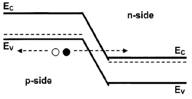
I2: Band To Band tunneling current (BTBC) –
If high electric field is applied across the
reverse biased diode, electrons tunnel from
valence band of p – region to the
conduction band of n – region.
Figure 2 Band to band tunneling in reverse
biased pn Junction4
I3: Punch through – It occurs when the
depletion width of drain side and the source
side sum up to the physical length of the
physical length of the body. Channel length
is increased as Vds is increased due to
depletion region. When this extends the
extreme case channel vanishes and
electrons punch through.
I4: Gate oxide tunneling – This takes place
due to direct tunneling between gate and
substrate of a MOSFET. When the transistor
is in ON state, gate oxide leakage is high
and will appear between gate and channel.
DYNAMIC POWER DISSIPATION
The dynamic power is mainly due to
charging and discharging of the capacitance
and the component of power which is
Available Online At www.ijpret.com the dynamic power. Dynamic power
consists of three components:
(i)Switching power - It is defined as the
power consumed by the logic state to
charge the output load from the low
voltage level to the high voltage level. It is
expressed as
Pswitching = Fswitching . Vdd2.CL (1)
(ii) Short circuit power - It is power passing
from power supply to ground when there is
a transition from logic “0” to logic “1”. It is
calculated as
PSc = Isc. Vdd (2)
(iii) Glitching power – It is the power
dissipated in intermediate transitions
during evaluation of logic function. It is
expressed as .
Pglitch = Vdd2. CL.VGlitch (3)
III. RELATED WORK
Dynamic domino logic is mostly used in
modern VLSI design. These circuits are
normally preferred over the conventional
logic circuit because of their high speed and
high performance. The main drawback of
this dynamic logic is it is susceptible to
noise and has increased power dissipation.
RBB technique is mainly used in standby
mode. Standby mode is the mode which the
circuit is idle, when subjected to idle
temperature and power supply variation.
In7, authors have applied the circuit to
different temperature and power supply
and found that sub threshold current is
reduced by applying the negative bias.
Alternatively RBB can be applied to idle
portion of circuit to reduce active leakage
power without compromising the speed8.
When a RBB is applied to MOSFET, junction
leakage is negligible compared to current
due to band to band tunneling9. The BTBT is
the dominant component in junction
leakage current is reduced by applying RBB,
which significantly reduces the sub
threshold leakage current8. In this paper,
we present a new methodology for Reverse
body bias technique to improve the
robustness and high performance, thereby
Available Online At www.ijpret.com BODY BIASING
Body biasing is the other method of
improving energy/efficiency by regaining
the performance lost. It involves connecting
the transistor bodies to a bias network
rather than to a source or ground. The body
biasing can be done internally (On-Chip) or
Externally (Off-chip). Reverse body bias
involve applying a negative body-to-source
voltage to an n-channel transistor, thereby
raising the threshold voltage and making
the transistor slower and less leaky.
Forward body bias, on the other hand,
lowers the threshold voltage by applying a
positive body-to-source voltage to an
n-channel transistor and thereby makes the
transistor both faster and leakier.
Figure 3 Reverse body bias circuit a) NMOS
transistor b) PMOS transistor5
In this paper reverse body biasing technique
is used. The body bias technique increases
the threshold voltage by applying negative
voltage across the source to substrate
junction as shown in Fig.3. The positive
charge on the gate is balanced by the
charge on the inversion region and negative
charge in the depletion region. When the
MOSFET is reverse biased, width of
depletion region increases, which increase
the charge of plate of MOS capacitor as
shown in Figure 4.
Figure 4 Reverse body biased NMOS
transistor6
In order to maintain the charge balance, the
electrons in the inversion layer is reduced,
as a result of which the gate voltage is
increased to maintain the similar level of
charge inversion as in zero body biased
MOSFET. Thus the magnitude of the
threshold voltage increases due to reverse
bias. Thus RBB technique can be used in
standby mode to increase the threshold
voltage, thereby reducing the sub threshold
Available Online At www.ijpret.com under different body biasing condition can
be calculated by the following formula.
=
V 0 + √ −2∅ + | − (√| − 2∅ |) (4)
The parameter γ (gamma) is called the
body-effect coefficient, and expresses the
impact of changes in VSB. The threshold
voltage has a positive value for a typical
NMOS device, while it is negative for a
normal PMOS transistor.
METHODOLOGY
Dynamic logic is widely used in modern VLSI
techniques since they are often favored by
high speed and performance with rising
edge delay. This paper discusses several
domino circuit techniques to reduce the
power dissipation while simultaneously
improving the noise immunity. Reverse
biasing can be used to increase the
threshold voltage thereby reducing the sub
threshold leakage current. As the threshold
voltage is increased through body biasing,
sub threshold leakage reduces. In the case
where the PMOS is connected to the clock
during the pre charge phase suffers loss of
charge due to leakage and charge
distribution. This problem can be resolved
by connecting the keeper PMOS parallel to
pull up network.
Figure 5 CMOS inverter with conventional
body bias
Figure 6 CMOS inverter with Reverse body
bias
Essentially, the sub threshold leakage gets
reduced when threshold is increased and
this can be achieved by connecting the body
to either power supply rails or ground.
Biasing the body below the source for
Available Online At www.ijpret.com increase the magnitude of the threshold
voltage. To do so, we allow two connections
for body. Here PMOS transistor is used for
body biasing, since there is one ground and
two power supplies available. One power
supply is at higher potential and other at
the lower potential.
Figure 7 CMOS inverter with proposed
Reverse bias
When the enable signal is asserted high,
~en will be low which turns ON the PMOS
device that is tied to the body of the core
circuit’s PMOS device. When en is de
asserted low, ~en will be pulled high and
turn off this connection. In its place, the
secondary PMOS device will pull the core
body connection to VDD, effectively
increasing the magnitude of the Vt of the
core PMOS device, and thus reducing
leakage in the inverter. The main difficulty
with the above technique is that it requires
a separate connection for the PMOS body.
Typically, in standard cell logic, the body is
directly connected to supply. There is also a
risk that if these body-connecting PMOS
devices have too large of an on-resistance,
they can cause latch-up. However, the size
of the resulting PMOS devices in this case
would still be much less than that required
of an equivalent PMOS supply switch. One
of the main benefits of the reverse body
bias technique is that it allows for circuits
which hold state.
SIMULATION RESULTS
The proposed reverse body bias technique
is implemented using CAD tools in 45nm
technology at 250c. The basic conventional
inverter is compared with the proposed
logic. Finally all these circuits are compared
for their power, delay and power delay
product. The designed reverse biased
inverter shows better performance in terms
of speed but has the constraint of noise.
Figure 8 shows the comparison among the
conventional and the proposed logic styles
in terms of power. Figure 9 shows the delay
Available Online At www.ijpret.com CONCLUSIONS
We have proposed new reverse body bias
logic with reduced power and also with
higher speed with the compromise of noise.
The proposed circuit uses small PMOS
transistor in its leakage path to reduce the
power consumption. The result of the
circuit was compared with the conventional
approach of body biasing. It provides better
performance than the previous approach.
References
1. S Borkar, Low Power Design Challenges
for the Decade. Proceedings of the
IEEE/ACM Design Automation Conference,
2001, pp. 293-296.
2. P Srivastava, A Pua, and L. Welch, .Issues
in the Design of Domino Logic Circuits,.
Proceedings of the IEEE Great Lakes
Symposium on VLSI, pp. 108-112, February
1998.
3. A Keshavarzi, Ki Roy and CK Hawkins,
Intrinsic leakage in deep submicron CMOS
ICs: Measurement based test solution, IEEE
transaction on VLSI systems. 2000; 8(6):
717–723.
4. Y Taur and TH Ning, Fundamentals of
modern VLSI design, Cambridge University
press.
5. CMOS Digital Integrated Circuits Analysis
& Design by Sung-Mo Kang, Yusuf Leblebici.
6. N. Weste and K. Eshraghian, Principles of
CMOS VLSI design, Addison Wesley,
Reading, MA, 1993.
7. Kuroda T, A 0.9V, 150 MHz, 10- mW, 4
mm2, 2D discrete cosine transform core
processor with Variable Threshold voltage
scheme. IEEE Journal of Solid state Circuits.
8. A Keshavarzi, Effectiveness of reverse
bias for leakage control in scaled dual- Vt
CMOS ICs. Proceedings of IEEE international
Symposium on Low Power Electronics and
design.
9. A Keshavarzi, Technology scaling
behavior of optimum reverses standby
leakage power reduction in CMOS IC’s. 0
0.001 0.002 0.003 0.004 0.005
Po
w
e
r
in
m
ic
ro
w
a
tt
Power
Available Online At www.ijpret.com
Proceeding of the IEEE international on low power electronics and design.