Volume 2, Issue 4, 2015
58 Available online at www.ijiere.com
International Journal of Innovative and Emerging
Research in Engineering
e-ISSN: 2394 – 3343 p-ISSN: 2394 – 5494
External Memory Interface with PIC microcontroller
Ashutosh Tripathi
1, Mahendra Singh
1, Amit Kumar Singh
1, Sushma R Wadar
2, Avinash Patil
21BE E&TC Students, Army Institute of Technology, Pune (MH), India
2Asst. Prof, Army Institute of Technology, Pune (MH), India
ABSTRACT:
PIC microcontroller like all other microcontrollers have two different kinds of memory, a non-volatile memory for storing firmware and a volatile memory for temporary data. We propose analysis of architecture of PIC16F84A and a modified architecture and op-code table for PIC16F84A to interface it with external memory in this paper. This model is developed by using VHDL, simulation results have been verified. It is observed that interfaced external memory can be used by using this model without affecting its performance.
Keywords:Op-Code, ALE, R/W’, CS’,VHDL.
I. INTRODUCTION
The PIC16F84A belongs to mid range family of PIC microcontrollers. There are two memory blocks in PIC1684A, program memory and data memory. It has 68 bytes of data RAM and 64 bytes of data EEPROM [5]. It has total
18 pins in which 13 are dedicated for input and output [5]. The first thing we need for memory interfacing is ALE and
Read/Write pin. There is no provision for interfacing external memory with PIC16F84A.
Figure 1: Architecture of PIC16F84 microcontroller [5]
Volume 2, Issue 4, 2015
59 It has 35 instruction set of 14bit op-code [5]. One of these instructions set op-code has to be modified so that two
new instruction set for read and write can be created.
II. EARLIERWAYSFORINTERFACING
Earlier ways used for interfacing with PIC family micro-controller is through SPI communication which uses master-slave concept [3]. The interfacing diagram is given below.
Figure 2: Interfacing using SPI communication [3]
This type of communication to interface external memory is very slow. The functions of various signals are given below.
Table 1: SPI communication signals function [3]
SIGNALS FUNCTIONS
SCLK It’s synchronous clock SS It’s used for slave select MOSI Master Output Slave Input MISO Master Input Slave Output
It uses 8-cycle for 8-bit transfer of data from master to slave or slave to master. 1-bit each time, so 8-bit address=1x8=8 cycle
8-bit data = 1x8=8 cycle Total =16 cycle= 64T state
(Either for read or write)
So total =32 cycle (128T state) for both reading and writing one byte.
It’s very time consuming and can’t be used in real time applications, where time is very important factor. So, we are trying to implement it in parallel way to achieve, external memory interface in less cycle.
III.DESIGNANDIMPLEMENTATION
A. Modified Architecture
Generalized interfacing diagram for external memory is given below. It provides parallel interfacing which provides faster access and can be used in real time applications [3].
Figure 3: General external memory interfacing [1]
Important pins for interfacing the memory are ALE, Read/Write, Address lines (AD0-AD7).
ALE is used for latching the address to the memory at T1 state of the clock. If ALE is ‘1’ or high then address will be latched to the memory. R/W’ decides whether the data is to read from the memory or write to the memory. If R/W’ = ‘1’ or high then microcontroller is going read data from memory. If R/W’ = ‘0’ or low then microcontroller is going to write to memory. CS’ decides whether our operation is external memory related or normal execution. If CS’=0 then operation is related to the external memory otherwise it is a normal execution.
PIC16F84A microcontroller doesn’t have these pins (ALE and R/W’). So in order to have these two pins we have to modify the available 13 input/output pins. In order to include these, architecture of PIC16F84A microcontroller is modified. This proposed architecture have ALE, R/W’ and CS’ multiplexed with RA3, RA2, RA1 (I/O pins of port A). All
I/O pins of port B will work as address data lines (AD0 - AD7).
Volume 2, Issue 4, 2015
60 Given below is the table showing signals required and their function while establishing external memory interface with microcontroller.
Table 2: Signals required and their functions [3]
SIGNALS FUNCTIONS
AD0-AD7 8-bit Data and 8-bits of Address are multiplexed
ALE Address Latch Enable Signal to latch the multiplexed address in the first clock cycle.
CS’ Chip select line is made low to access the external memory chip
R/W’ It is used for read/write If R/W’=0, then used for write. If R/W’=1, then used for read.
The modified architecture which we proposed is given below.
Figure 4: Modified architecture of PIC16F84
B. Introducing 2- new Instructions
PIC16F84A have 35 instruction sets of 14-bits of op-code, and there is requirement of two new instruction sets for read and write. So we have modified the op-code of MOVLW (move literal to W-register).
Table 3: MOVLW Op-code [5]
Mnemonic 14-bit Op-code
MSB LSB MOVLW 1 1 0 0 X X F F F F F F F F
Volume 2, Issue 4, 2015
61
Table 4: Modified Op-code with new Instructions
Mnemonics 14-bit Op-code
MSB LSB MOVLW 1 1 0 0 0 0 F F F F F F F F MOVXR 1 1 0 0 0 1 F F F F F F F F MOVXW 1 1 0 0 1 0 F F F F F F F F
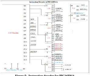
C. Modification of Instruction Decoder
Whenever an instruction is entered, instruction decoder decodes its equivalent op-code and performs the task. This microcontroller has 35 instruction sets so it uses 4:16 decoder. Out of 14-bits op-code, 6-bits decide the instruction and remaining 8-bits are either for literals value or for memory location. The select lines of 4:16 decoder use 13-10 op-code bits. This decoder is further decoded to get all the instruction sets.
The required instruction gets activated on the decoder output, and performs its equivalent task. Instruction decoder for PIC16F84A is given below.
Figure 5: Instruction decoder for PIC16F84A
The D12 output of 4:16 decoder corresponds to MOVLW instructions. It further use 2:4 decoder which uses 9&8 op-code
bits as select lines to generate 4 new instructions.
Table 5: New instruction and their functions
INSTRUCTION FUNCTION
MOVLW Move literals to W-register
MOVXR Move data from external memory.(Reading) MOVXW Move data to external memory(Writing) Reserved Can be used in future.
Modification done in instruction decoder circuit is shown below to get above discussed instructions.
Figure 6: Modified Decoder corresponds to MOVLW
D. I/O port architecture
Volume 2, Issue 4, 2015
62
Figure 7: I/O port architecture of Port A (RA0 – RA3) [5]
To provide the facility of external memory interfacing, this port architecture needs to be modified. All three extra pins(ALE, R/W’, CS’) which are necessary for interfacing external memory, are multiplexed with Port A.
Figure 8: Modified port architecture Port A.0
Proposed port architecture is given above for a pin of PORTA so that whenever an external memory related instruction is called, it uses this architecture.
Out of available pins of PORTA, we multiplexed RA.3 with ALE, RA.2 with R/W’ and RA.1 with CS’.
E. Algorithm
Volume 2, Issue 4, 2015
63 it’s for read then send the address to the memory and data to be read from memory, if it’s for write then send the address to the memory and write the data to that memory location. If it’s normal instruction then proceed for normal execution. Check repeatedly for memory instruction, otherwise execute normal instruction and stop when end of program reached.
Figure 9: Algorithm for external memory interfacing
F. T-state WORKING
PIC16F84A microcontroller uses pipelining concept, in which it divides the work into smaller modules so that execution speed can be increased. It has 4 MHz crystal frequency which is divided into 4-T state [5]. The working of 4-T
state is given below.
Figure 10: Working of T-state diagram
In T1-state, it fetches the instruction. In T2-state, it decodes the instruction. In T3-state, it executes the instruc-tions. In T4-state, it writes back the result.
IV.RESULTANDSIMULATION
This is how the crystal frequency of microcontroller is divided into 4-T state to execute more no of instructions and make execution faster. Its simulation is given below.
Volume 2, Issue 4, 2015
64 The RTL schematic of VHDL code which we have designed is given below. Here command, data_in, clk act as input and ale, rd, wr, data_addr as output. Command input is used to give the opcode of the desired instruction. Data_in input is taking data which is to be written. Ale, rd, wr is used for address latch enable, for read or write respectively.
Figure 12: RTL schematic for External memory interface module
The output waveform of this code, is given below
Figure 13: Output waveform for external memory interface module
We have verified the VHDL code for read and write opcode and are working properly. This model is taking 4-machine cycle for reading or writing one byte which is much far better than using SPI communication interfacing which is taking 32-machine cycles.
CONCLUSION
We have designed a model which provides the facility to interface external memory with PIC16F84A. The proposed model has been verified using VHDL code, and is working properly for the designed op-code of read and write.
REFERENCES
[1] A PIC compatible RISC CPU core Implementation for FPGA based for Embedded Applications - Haritha Madasi, S Nagakishore Bhavanam, and Vaujadevi Midasala.
[2] An External Memory Interface for FPGA-Based Computing Engines - Joonseok Park and Pedro Dinis. [3] External Memory Interfacing Techniques for the PIC18F8XXX - Tim Rovnak.
![Figure 1: Architecture of PIC16F84 microcontroller [5]](https://thumb-us.123doks.com/thumbv2/123dok_us/8873946.1815720/1.595.138.444.400.682/figure-architecture-pic-f-microcontroller.webp)
![Figure 3: General external memory interfacing [1]](https://thumb-us.123doks.com/thumbv2/123dok_us/8873946.1815720/2.595.176.420.521.642/figure-general-external-memory-interfacing.webp)

![Figure 7: I/O port architecture of Port A (RA0 – RA3) [5]](https://thumb-us.123doks.com/thumbv2/123dok_us/8873946.1815720/5.595.120.476.354.683/figure-port-architecture-of-port-ra-ra.webp)


