ScholarWorks@UNO
ScholarWorks@UNO
University of New Orleans Theses and
Dissertations Dissertations and Theses
12-15-2006
Angle Resolved Photoemission Study of Epitaxial Chromium
Angle Resolved Photoemission Study of Epitaxial Chromium
Dioxide Films
Dioxide Films
Daniel Borst
University of New Orleans
Follow this and additional works at: https://scholarworks.uno.edu/td
Recommended Citation Recommended Citation
Borst, Daniel, "Angle Resolved Photoemission Study of Epitaxial Chromium Dioxide Films" (2006). University of New Orleans Theses and Dissertations. 481.
https://scholarworks.uno.edu/td/481
This Thesis is protected by copyright and/or related rights. It has been brought to you by ScholarWorks@UNO with permission from the rights-holder(s). You are free to use this Thesis in any way that is permitted by the copyright and related rights legislation that applies to your use. For other uses you need to obtain permission from the rights-holder(s) directly, unless additional rights are indicated by a Creative Commons license in the record and/or on the work itself.
A Thesis
Submitted to the Graduate Faculty of the University of New Orleans in partial fulfillment of the requirements for the degree of
Master of Science in
The Department of Physics
by
Daniel R. Borst
B.S. Purdue University, 2004
ii
iii
I would like to acknowledge my parents for their continuous love and support,
and for pushing me in the right direction.
I would like to thank Dr. Ventrice for his guidance and motivation. I am grateful
for his effort in acquiring the funding, time, and other resources required for my research
and academic experience. I would also like to express my thanks to Dr. Arun Gupta for
providing the samples for our research.
Thanks to my family and friends Heather, Jeff, Robin, Shalane, Ian, Giacamo,
Emily, Jeremy, Bob, and Natalie for their friendship, encouragement, advice, and
tolerance. I would also like to thank Michelle and Christy for providing the necessary
caffeine for my master’s thesis and rapidly approaching deadlines, and Sandra for sharing
my lack of enthusiasm for paperwork.
I would like to thank Dr. Sprunger, Dr. Losovich, and Dr. Geisler for their
encouragement and expertise.
I extend my gratitude to Purdue University, the U.N.O and L.S.U physics
iv
LIST OF FIGURES ... vi
LIST OF TABLES ... viii
ABSTRACT... ix
1. INTRODUCTION ... 1
1.1 Motivation ... 1
1.2 Background Information and Previous Work ... 1
1.3 Present Work... 3
2. EXPERIMENTAL DETAILS ... 5
2.1 Ultra-High Vacuum ... 5
2.2 Angle-Resolved Photoemission... 7
2.3 Low Energy Electron Diffraction (LEED)... 13
2.5 Sample Preparation ... 19
3. RESULTS AND DISCUSSION ... 21
3.1 Spin-resolved Electronic Structure Calculations ... 21
3.2Angle-resolved Ultraviolet Photoemission Measurements... 26
3.2.1 CrO2(100) ... 26
3.2.2 CrO2(110) ... 30
3.2.3 Dry Scroll Pump ... 33
3.3 CrO2 LEED ... 35
3.5 Chromium Oxide Density of States Integration ... 36
3.5.1 Integration Procedure... 36
v
REFERENCES ... 43
vi
Fig. 1.1 Spin polarization of the density of states of CrO2 ...3
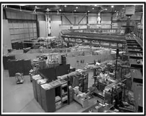
Fig. 1.2 CAMD Experimental Hall ...4
Fig. 2.1 Photoemission energy density diagram from samarium ...8
Fig. 2.2 Universal curve of electron mean free path ...9
Fig. 2.3 The emission of photoelectrons ...10
Fig. 2.4 Photoionization diagram ...11
Fig. 2.5 Energy level diagram for photoelectron spectroscopy ...12
Fig. 2.6 Schematic of a 4 grid LEED system as a retarding field analyzer ...13
Fig. 2.7 A linear array of in-phase coherent oscillators ...14
Fig. 2.8 The path difference for two arbitrary scattering centers ...15
Fig. 2.9 Several LEED pattern examples ...18
Fig. 2.10 Photograph of sample holder and crystal ...19
Fig. 3.1 Calculated spin-resolved density of states for CrO2 ...22
Fig. 3.2 Calculated spin-resolved density of states for Cr2O3 ...23
Fig. 3.3 Total density of states for CrO2 ...24
Fig. 3.4 Total density of states for Cr2O3 ...25
Fig. 3.5 CrO2 (100) core spectra ...28
Fig. 3.6 CrO2 (100) valence spectra ...29
Fig. 3.7 CrO2 (110) core spectra ...31
Fig. 3.8 CrO2 (110) valence spectra ...32
Fig. 3.9 CrO2(100) core electron spectra with dry scroll pump ...34
vii
Fig. 3.12 Actual CrO2(100) core electron spectrum ...36
Fig. 3.13 CrO2(100) core electron spectrum after peak removal ...37
Fig. 3.14 CrO2(100) core electron background signal with polynomial fit ...38
Fig. 3.15 Actual CrO2(100) core electron spectrum with polynomial fit ...38
viii
ix
Chromium dioxide is predicted to be a half-metallic oxide. The electronic
properties of the surface region of CrO2 have been studied by performing angle-resolved
ultra-violet photoelectron spectroscopy (ARUPS) measurements on epitaxial CrO2 films.
The CrO2 thin films were deposited on (100) and (110) – oriented TiO2 substrates by
chemical vapor deposition. Previous measurements of the transport properties of devices
made from epitaxial CrO2 films have shown very little spin polarization. Possible
sources of this low yield are a surface Cr2O3 phase and/or surface contamination. The
effects of sputtering the CrO2 films to remove the outer layer of Cr2O3 and any surface
contaminants and of annealing the films in oxygen to heal surface were examined. The
ARUPS spectra of the CrO2 films have been compared to epitaxial Cr2O3 films prepared
on Pt(111). In addition, low energy electron diffraction patterns of the sputtered and
annealed CrO2 films have been prepared indicating that the surface remains in a CrO2
1
1. INTRODUCTION
1.1 Motivation
The recently discovered phenomenon of half-metallic behavior has attracted
considerable attention in the context of rapidly emerging fields of spin-polarization
electronics (spintronics). Half-metals simultaneously exhibit conducting and insulating
properties, with the unusual effect of being metallic for electrons sharing the same spin
direction, and insulating for electrons with the opposite spin direction [8]. The resulting
magnetic moment is already being explored for use in semiconductor and nanoscale
technologies such as magnetic random access memory (MRAM), and spin momentum
transfer (SMT). In particular, CrO2 films are attractive due to the predicted high spin-
polarization near the Fermi level. Spin polarized conduction studies are yielding
promising results for device fabrication in speed, size, selectivity, and power as the
boundaries of more traditional methods are being realized.
The effect of magnetoresistance, or the ability for a substance to change its
resistance based on applied magnetic fields, is also being explored. Giant
magnetoresistance (GMR) offers the possibilities of memory devices with superior
storage capabilities with the advantage of being immune to power interruptions and
ionizing radiation – an appealing prospect for military and space applications. Tunnel
magnetoresistance (TMR) is another developing area in electron control, based on the
crystal’s magnetic bias as theory indicates improved semiconductor properties.
1.2 Background Information and Previous Work
Although a number of theoretically predicted half-metallic materials have been
2
confirmed. The metastable nature of the film frequently results in the formation of a
natural Cr2O3 on the CrO2 surface, because it is, thermodynamically, much more stable.
High-resolution microscopic studies have verified the occurrence of the lattice matched
hexagonal corundum structure of Cr2O3 on the CrO2 surface [10,13]. It is questionable as
to what causes the spontaneous growth of the undesired layer, or when it is formed.
Because it is metastable, CrO2 will irreversibly reduce to Cr2O3 at high temperatures and
atmospheric pressure. As expected, temperature constraints must be considered when
dealing with metastable heterostructures. It is unclear whether the reduced layer forms
immediately after film growth termination or after exposure to the atmosphere [10,13].
Theoretical studies predict the CrO2 half-metal to have a full spin-polarization of
100% as shown in Fig. 1.1. Samples examined in previous studies grown by chemical
vapor deposition (CVD) with chromyl chloride (CrO2Cl2) as a liquid precursor, yielded
atomically smooth films with spin polarizations of 98.4% [13]. Magnetization and
resistivity measurements were comparable to the fabrication group’s more cumbersome
methods involving CrO3 powder as a solid precursor. As such, CVD is the preferred
fabrication technique for CrO2 crystal growth for most CrO2 spin-polarization research
[9].
3 1.3 Present Work
The present study focuses on the properties of epitaxial CrO2 thin films grown on
TiO2 as a template. TiO2 is an excellent foundation for epitaxial growth since the
substrate cuts of various orientations are available and the lattice mismatch is only about
4%. From our LEED and photoemission measurements that were taken after a variety of
sputtering and annealing cycles, the films show a surprisingly stable film structure with
no indications of major surface reduction. Photoemission measurements taken
demonstrate that the oxygen and chromium concentrations maintain their initial atomic
ratio under the conditions used in these experiments and are not as sensitive as
anticipated.
Hydrocarbon contamination can become prevalent at some point during the film
growth, atmosphere exposure, or vacuum analysis. To reduce the presence of oils and
lubricants, a dry scroll pump was temporarily implemented to possibly provide insight
into the hydrocarbon’s origin. The hydrocarbon contamination showed no attenuation
and appears to be present before vacuum analysis. As with earlier studies, a shift in the
Fermi level of CrO2 occurs after sputtering, which is probably due to slight changes in the
stoichiometry of the surface. All photoemission and LEED measurements were taken at
the CAMD synchrotron in Baton Rouge, Louisiana. A picture of the CAMD
4
5
2. EXPERIMENTAL DETAILS
2.1 Ultra-High Vacuum
Clean surfaces are generally very reactive towards impinging particles from
residual gas mixtures similar to that existing in normal atmospheric conditions. The
sensitivity of clean surfaces as such requires a well-controlled environment in which the
effects of undesirable surface contamination reactions and alterations can be minimized.
By maintaining a clean contamination free surface, it can be studied with the advantage
of obtaining repeatable results. Most systems are equipped with a number of
measurement devices capable of controlling other conditions, such as temperature and
deposition rates. Kinetic gas theory indicates that the number of particles colliding with a
surface per unit time and areais determined by
dn dt ffffffff f g s =1 4 ffffN g v ffff (2.1.1)
where Ng is the number of gas molecules per cm3 and v ffff
is their average thermal velocity.
It then follows that
dn dt ffffffff
f g
s
=Ng
RT 2πM
ffffffffffffffff
swwwwwwwwwwwwwwwwwwwwwwwwwwwwwwwwwwwwwwwwwwwwwwwwwwwwwwwwwwwwwwwwwwwwwwwwwwww≈ 3.5A1022 P MT
pwfffffffffffffffffffwwwwwwwwwwwwwwwwwwwwwwwwwwwwwwwwwwwwwwwwwwwwww cm@2s@1
B C
(2.1.2)
where
R = gas constant T = absolute temperature
M = molecular weight and P = gas pressure in Torr.
Assuming a monolayer capacity of 3.5A1014 particles/ cm2, at temperature T = 300 K, and
6 dn dt ffffffff f g s
≈106AP monolayers/ sB C . (2.1.3)
Consequently, at 760 Torr (atmospheric conditions) the number of molecules needed to
assemble a monolayer is offered to a surface almost every nanosecond. At a pressure of
10@6 Torr (standard high vacuum conditions) the time necessary for a surface to build a
monolayer is reduced to 1 second. Monolayer construction also depends on the
probability that impinging molecules will be accepted, which is called the sticking
coefficient ‘s’. This is quite often close to unity for reactive surfaces such as Si. It is
clear that much lower pressures are critical for surface research [4].
Ultra-high vacuum systems are capable of achieving pressures less than 10-10
Torr, which is ultimately determined by gases emitted from the materials used to build
the apparatus itself [4]. Since most spectroscopic techniques are also capable of detecting
molecules in the gas phase, the number of particles present on the surface should
substantially exceed those present in the gas phase immediately above the surface [6].
The mean free path, λ, is defined as the average distance traveled by a particle
between collisions
λ = kT 2
pwfffffffffffffffffffffffwwwwwwwwwwwwwwwwPσ (2.1.4)
where
k = Boltzmann’s constant ( = 1.38 x 10⁻²³ J/K) T = temperature [ K ]
P = pressure [ N/m2 ]
σ = collision cross section [ m2 ].
Low-pressure atmospheres allow the use of various electron- and ion-based measurement
7
phase scattering and allowing relatively uninterrupted particle flow to and from the
surface [11].
2.2 Angle-Resolved Photoemission
Photoemission is the release of electrons from a material by means of a photon
in/electron out energy transfer process. Photoemission techniques are capable of
extracting atomic information about surfaces through the use of this relationship by
analyzing the kinetic energy of photoemitted electrons. Photoelectron spectroscopy for
material studies is typically broken into two branches, classified by the source of exciting
radiation: ultraviolet and X-ray photoelectron spectroscopy (UPS and XPS, respectively).
Taking advantage of these different radiation energies provides valuable information
about electron binding energies within a material. In UPS, ultraviolet radiation (<200
eV) is used to examine valence electron properties, while the higher energy soft X-rays
(200-5000 eV) employed in XPS can be used to probe deeper into the atom, revealing
core level electron properties [2]. By examining the binding energies of electrons of
various materials, spectroscopy exposes not only the atoms present in a material, but also
their relative ratio, or stoichiometry, thus identifying molecules within the material. XPS
8
Fig. 2.1 Photoemission energy density diagram from the f-shell of samarium. The UPS spectrum is more surface sensitive than the XPS results [2].
Both methods ionize secondary electrons beneath the surface as a consequence of the
light source being able to penetrate farther into the surface than the mean free path of the
primary electrons, resulting in inelastic scattering, and creating a background signal onto
which the surface signal is constructed. The inelastic mean free path of electrons in a
9
Fig. 2.2 Universal curve of electron mean free path [2]
The photoionization process can be described by considering momentum transfers
at the atomic level and making use of the conservation of energy principle. Einstein and
Planck determined that the energy of a photon is proportional to the frequency of the
radiation, and is given by Einstein’s relation
E =hv (2.2.1)
where
h = Planck’s constant (6.62x10⁻³⁴ JAs) v = frequency of radiation [Hz].
Conservation of energy requires that the kinetic energy of the escaping photoelectron
added to the amount of energy required to release the electron, or binding energy, is equal
to the energy of the incoming photon, or
10
where the binding energies of electrons are usually referenced to the Fermi level.
Therefore there is a barrier for photoemission W = qϕ that results for the work function
ϕ of the crystal. This describes a photon in/electron out process, whereby the specific
electron binding energies provide information about the atomic arrangements. Several
photoemission scenarios are illustrated in Fig. 2.3.
Fig. 2.3The emission of photoelectrons [1]
A schematic of the photoemission experimental geometry is shown in Fig. 2.4. Since the
photoelectron’s kinetic energy is measured at the spectrometer, its measured kinetic
energy is referenced to the work function of the spectrometer, not the sample. This is
11
12
13 2.3 Low Energy Electron Diffraction (LEED)
LEED analysis involves the use of a beam of electrons of well-defined energy
incident normal to a surface. Electrons from the beam are scattered back toward a
phosphor coated screen creating a diffraction pattern, rendering information about the
spacing, symmetry, and alignment of the sample’s unit cell and geometric structure. A
schematic of a LEED optics system is shown below.
Fig. 2.6Typical schematic of a 4 grid LEED system as a retarding field analyzer [4]
With the appropriate wavelength, the backscattered electron beams from
well-ordered surfaces generate a pattern identifying specific molecular orientations.
14
waves normal to the sample. Surface atoms are treated as a plane of point scatterers, as
shown in figure 2.7.
Fig 2.7 A linear array of in-phase coherent oscillators [12]
The de Broglie wavelength, λ, written in terms of Planck’s constant, h, and the
electron momentum p, is defined as
λ = h p
fffff . (2.3.1)
The relationship can be rewritten in terms of the elementary electron charge, e, electron
mass, m, and the acceleration voltage, V, as
λ = h
2mAeAV
pwfffffffffffffffffffffffffffffffffffwwwwwwwwwwwwwwwwwwwwwwwwwwwwwwwwwwwwwwwwwwwwwwwwwwwwwwwwwwwwwwwwwwwwwwwwwwwwwwwwwwwwwwwwwwwwwwwwwwwwwwwwwwwwww . (2.3.2)
Thus, electron energies on the order of 150 eV have a wavelength of approximately 1 Å,
15
typically in the range of 10 – 475eV, corresponding to a wavelength range of 3.9 to .56
Å. Low energy electrons are ideal for surface analysis as they penetrate only the first few
layers (~ 5 Å) of a substrate. As a result, the emerging diffraction patterns characterize
the reciprocal lattice, the projection of reciprocal vectors defined by two-dimensional
surface vectors.
The von Laue formulation assumes that sets of atoms in a Bravais lattice radiate
the incident radiation at the same frequency in all directions. As a consequence, the
radiation interferes constructively, producing the diffraction maxima. The geometry of
two scattering centers separated by a distance d where the incident and scattered radiation
have wave vectors kjjkjjjjjjjjand kkjjjjjjjjjj., respectively, in the directions of the unit vectors eˆ and ˆe',
respectively (eˆ a kjkjjjjjjjjj/ | kkjjjjjjjjjj| ,etc.). Thus, k=2πeˆ/λ and k. =2πeˆ’/λ. This is
diagrammed in the figure below.
16 The path difference is
d sinθ +d sinθ. =kjjdjjjjjjjjA (eˆ - ˆe') (2.3.3)
and
d jjjjjjjjjj k
Abkjkjjjjjjjjj@kjjjjkjjjjjj.c =2πn (2.3.4)
where n is any integer. Therefore, when the path difference is an integral number, n, of
wavelengths then constructive interference occurs. By using the Bravais translation
vector it is possible to describe the constructive interference from an entire plane of
scattering elements, as illustrated in Fig. 2.7 [12]. The translation vector for a 3–
Dimensional crystal is defined as
tm
jjjjjjjjkjjjjjjjjjj=m
1kjajjjjjjj+m2b
j jjjjjjj k+
m3kjjcjjjj (2.3.5)
where akjjjjjjjj, bkjjjjjjjj,and ckjjjjjj are three arbitrary, independent vectors, and mi is any integer. Then
tm
jjjjjjjjjjjjkjjjjjjjjjj
Abkjkjjjjjjjjj@kjjjjkjjjjjj.c=2πn. (2.3.6)
This expression can also be written in the equivalent form
ei k jjjjjj k
@kkjjjjjj.
b c
Atm
j jjjjjjjkjjjjjj
= 1 . (2.3.7)
The set of wave vectors Kjjjjjjkjjjjjjjjjjjj = kkjjjjjjjjjj@kjjkjjjjjjjj. that satisfy the above equation is called the
reciprocal lattice, and is generated by three primitive reciprocal lattice vectors
a
jjjjjjjj k* =
2π b
jjjjjjjj k
Bkjjcjjjj
a
jjjjjjjj
kfffffffffffffffffffffffffffffAbkjjbjjjjjjBkjjjjcjjc , b
j jjjjjjj k* =
2π c
jjjjjj kBkjjajjjjjj
a
jjjjjjjj
kfffffffffffffffffffffffffffffAbkjjjbjjjjjBkjjjcjjjc , ckjjjjjj * =
2π a
j jjjjjjj kBkjjbjjjjjj
a
j jjjjjjj
kfffffffffffffffffffffffffffffAbkjbjjjjjjjBkjjjcjjjc (2.3.8)
where akjjjjjjjj, bkjjjjjjjj, and ckjjjjjj are the primitive lattice vectors. For example, for a simple-cubic
Bravais lattice, with a primitive cell of size a,
a jjjjjjjj
k=ax^, kjjbjjjjjj=a y^, kjcjjjjj=az^ (2.3.9)
17 a
jjjjjjjj k*
= 2π a
ffffffff^x, kjjbjjjjjj* = 2π
a
ffffffffy^, kjjcjjjj* = 2π
a
ffffffffz^ (2.3.10)
Fig. 2.7 shows plane waves propagating from a linear array of in-phase coherent
oscillators in the direction of the reciprocal lattice vectors, resulting in a number of
diffraction spots, which construct the interference pattern [7,3,5]. Sample LEED patterns
18
19 2.5 Sample Preparation
The present study makes use of a variety of sputtering and annealing cycles under
vacuum conditions for surface preparation. Chromium dioxide films were sputtered with
argon for times ranging between 5 and 30 minutes, stripping the surface of its outermost
layers, and presumably contaminants, by introducing high voltages capable of
accelerating the argon ions admitted into the vacuum chamber toward the target film.
The damaged surface subsequently is ‘repaired’ by annealing at high temperatures (after
restoring UHV conditions), by which amorphous regions recrystallize [2]. However,
annealing can also result in driving impurities to the surface, resulting in contamination
of the upper layers. This effect is seen in our results, and is clearly a result of the liquid
precursor. As such, this procedure is most effective if repeated several times. A picture
of the CrO2(100) crystal mounted on a sample holder is shown in Fig. 2.10.
20
The CrO2 films were grown at the Univ. of Alabama by Prof. Arun Gupta’s
research group using a chemical vapor deposition (CVD) technique with a CrO2Cl2 liquid
precursor. The deposition reactor used consists of a quartz tube placed inside a furnace
and kept at 400º C. After being cleaned with a number of organic solvents and dilute
hydrofluoric acid, the TiO2 substrates onto which the CrO2 films are to be grown are
placed on a glass susceptor. The precursor is placed into a bubbler and held at 0º C. The
flow rate of the oxygen carrier gas is 40 cc3/min, resulting in a deposition rate of 72
Å/min. The procedure results in epitaxial films yielding actual spin polarizations near
21
3. RESULTS AND DISCUSSION
The theoretically predicted 100% spin polarization of CrO2 has, so far, not been a
reality in the field of epitaxial CrO2 device fabrication, as a possible result of crystal
reduction due to its’ meta-stable nature and/or surface contamination. The meta-stable
nature of CrO2 predicts eventual crystal reduction into the more stable form of Cr2O3. It
is possible to determine the occurrence of reduction and surface contamination by using
photoemission comparison techniques. By determining the relative ratio of elements for
photoemission results for the unknown chromium oxide states and comparing them to
known results it is possible to determine the molecular identity of the epitaxial film, and
possibly isolate the source of such low spin polarization yields for device fabrication.
3.1 Spin-resolved Electronic Structure Calculations
Electronic structure calculations performed by Dr. Johannes van Ek predict a
conductive magnetic moment for CrO2, suggesting a minority electron concentration
above the Fermi level, and a majority electron concentration below. The predicted
density of states for the reduced chromium oxide state of Cr2O3 indicates a
semiconductor with electron spins of both directions above the Fermi level, and does not
show any sign of spin polarization, making it suspect for the unimpressive device
transport properties observed. The predicted density of states results for CrO2 and Cr2O3
are illustrated in figures 3.1 and 3.2, respectively. Electrons above the Fermi level for
CrO2 are predominantly minority electrons of the same spin, predicting a near 100% spin
polarization for conducting electrons – a nearly ideal half-metal. On the other hand, the
symmetry of majority and minority electrons for energies above the Fermi level for Cr2O3
22
23
Fig. 3.2 Calculated spin-resolved density of states for Cr2O3
Since the photoemission measurements taken are not spin-resolved, comparisons
must be made relative to the total density of states – the sum of majority and minority
density of states multiplied by the Fermi function [10]. The total density of states for
CrO2 and Cr2O3 are shown in figures 3.3 and 3.4, respectively. Calculated results for
24
Cr2O3 predictions indicate insulating characteristics, as there are no occupied states
visible above the Fermi level.
25
26
3.2Angle-resolved Ultraviolet Photoemission Measurements
All photoemission measurements from CrO2 were taken at the TGM/3m beamline
of the CAMD synchrotron in Baton Rouge, Louisiana, with light at an angle of incidence
(ψ i) of 45º. Core and valence emission measurements were taken with polarized light
intensities of 120 eV and 75 eV, respectively. Spectra shown are presented as electron
count intensities normalized to the current in the synchrotron ring versus binding energy
relative to the Fermi level. The Cr2O3 spectra were taken at the NSLS synchrotron at
Brookhaven by Robbert et al., for a thin film grown on platinum and are displayed at the
top of each plot for convenient comparison [10]. Since the thermocouple is mounted on
the manipulator block, not directly on the crystal, temperatures are only accurate to ~100º
C.
3.2.1 CrO2(100)
Spectra taken for CrO2 cores at a photon energy of hv = 120 eV are shown in Fig
3.5. Before film preparation, the molybdenum 4p electrons from the sample holder and
tantalum 4f electrons from the wires fixing the sample to the holder are visible. After
annealing at 250º C in oxygen, the chromium oxide film begins to dominate the spectra,
and the presence of the chlorine 3s electrons from the liquid precursor is slightly
detected. This effect is observed before sputtering and is a result of residual impurities
being driven to the surface from annealing. Sputtering of the surface results in the
detection of distinct O-2s and Cr-3p peaks. Annealing at 450º C in 10-6 Torr of O2 results
in a slight increase of the chromium and oxygen peaks, and the peaks appear to be much
more defined about their appropriate binding energies. None of the spectra appear to
27
analysis distinguishing chromium dioxide phases involving peak integration is included
in section 3.4.
Valence emission measurements taken at a photon energy of 75 eV for
CrO2(100), shown in Fig. 3.6, are consistent with the results from core emission. The
film again demonstrates considerable sensitivity toward the initial sputter. Valence
features become more pronounced and the onset of emission shifts away from the Fermi
level. Annealing the sputtered film at 450º C in oxygen results in a shift of the onset back
toward the Fermi level. The phenomenon of the spontaneous shift of valence features
away from the Fermi level after sputtering is often observed in CrO2 studies and remains
unexplained. A suspect for the low polarization yield of CrO2 based devices is the
presence of hydrocarbons at the surface. Slight oxygen peaks are visible near higher
binding energies suggesting contamination from crystal growth, atmospheric exposure,
28
29
30 3.2.2 CrO2(110)
The core electron emission measurements for CrO2(110) are shown in Fig. 3.7.
The oxygen and chromium ratios are preserved throughout the initial sputter and three
subsequent annealing processes. Tantalum is detected throughout the entire sample
preparation, and chlorine becomes visible after annealing at 450º C, and is even more
prevalent after annealing at 600º C. Chromium and oxygen detection reduces after the
high temperature annealing at 600º C, but the aspect ratio is conserved. Residual chlorine
emission from the liquid precursor becomes more frequent after each anneal, as a result
of being driven into the surface film.
Valence emission shown in figure 3.8 indicates the presence of hydrocarbons and
chlorine throughout sample preparation. The film shows sensitivity toward sputtering,
and annealing at 600º C reduces the chromium and oxygen electron emission, as with the
core analysis. As opposed to the CrO2(100) orientation, the valence features of
CrO2(110) do not seem to shift after the initial sputter. The CrO2(110) orientation too
exhibits insulating qualities with a valence electron emission peak approximately 2 eV
below the Fermi level.
31
32
33 3.2.3 Dry Scroll Pump
Spectra taken with an oil-free dry scroll pump in place of the turbo pump are
included in figure 3.9. Intensity levels are comparable to previous results, suggesting that
the presence of hydrocarbons is not due to the turbo pump or vacuum apparatus, and is a
result of atmospheric exposure or crystal growth. It does not appear that the vacuum was
responsible for the hydrocarbon contamination detected on the films being studied.
Despite sample preparation, the spectra indicate a nonconductive CrO2 form with a
valence electron concentration approximately 2 eV below the Fermi level, and no
34
In
te
n
si
ty
(
a
rb
.
u
n
it
s)
50 40 30 20 10
Binding Energy (eV)
Cr 3p
O 2s
250ºC in O2
No Prep Sputter (10 min) 450ºC in O2
CrO
2(100)/TiO
2(100) Cores
hv = 120 eV
α = 45º
Normal Emission
No Prep (dry scroll)
35 3.3 CrO2 LEED
LEED results provide additional evidence for the CrO2 phase. The diffraction
pattern created by the chromium oxide film after annealing at 600º C is shown in Fig.
3.10. The pattern reveals the rectangular symmetry corresponding to the rutile structure
of CrO2(110) illustrated in figure 3.11.
Fig. 3.10 LEED - CrO2(110) after 600º C anneal
36 3.5 Chromium Oxide Density of States Integration
3.5.1 Integration Procedure
As mentioned earlier, comparing the ratio of elements for known and unknown
chromium oxide states is a useful method for determining the molecular phase of the
film. The relative number of states of chromium and oxygen is determined by integrating
the peaks in the core electron density of states spectra. Since the light source is capable
of penetrating farther into the surface than the mean free path of the primary electrons, a
background signal due to inelastic scattering of these secondary electrons is generated,
onto which the primary signal is added. Thus, the secondary signal must be subtracted
before integrating the peaks. The procedure used is outlined below.
1600 1400 1200 1000 800 In te n s it y 100 95 90 85 80 75 70 65
Binding Energy (eV)
37
An actual spectrum obtained for CrO2 grown on TiO2 is illustrated in figure 3.12.
First, the peaks are removed from the data to prepare the spectrum for a polynomial fit of
the secondary electron tail.
1000 950 900 850 800 750 700 In te n s it y 100 95 90 85 80 75 70 65
Binding Energy (eV)
Fig. 3.13 CrO2(100) core electron spectrum after peak removal
A third order polynomial is then fit to the data to approximate the background signal.
The polynomial fit is shown by the smooth line running through the data in figures 3.14
and 3.15. The original data with the background signal approximation is displayed in
38 1000 950 900 850 800 750 700 In te n s it y 100 95 90 85 80 75 70 65
Binding Energy (eV)
Fig. 3.14 CrO2(100) core electron background signal with polynomial fit
1600 1400 1200 1000 800 In te n s it y 100 95 90 85 80 75 70 65
Binding Energy (eV)
Fig. 3.15 Actual CrO2(100) core electron spectrum with polynomial fit
The primary core electron density of states signal, after subtracting the background signal
from the original data is shown in Fig. 3.16. Peak integration can now be performed to
determine the oxygen to chromium ratio of the primary electron signal representing the
39 800 600 400 200 0 In te n s it y 100 95 90 85 80 75 70 65
Binding Energy (eV)
Fig. 3.16 CrO2(100) core electron spectrum primary signal
The following Matlab script integrates the peaks and outputs the ratio of oxygen to
chromium states. The script uses a center-bound rectangular integration method of
averaging successive intensity values and generating rectangles followed by a
40
% Daniel Borst
% peak_spec - Program to integrate and compare spectrum peaks
clc; help peak_spec; % Clear command window and print header
% Initialize parameters
kinetic_e = input('\n\nEnter kinetic energy variable: '); raw_counts = input('Enter raw counts variable: ');
dt = kinetic_e(2) - kinetic_e(1); % Define rectangle width
% Plot raw counts vs. kinetic energy plot(kinetic_e,raw_counts);
% Isolate chromium peak
l_bound1 = input('\n\nEnter chromium left boundary: '); r_bound1 = input('Enter chromium right boundary: ');
% Isolate oxygen peak
l_bound2 = input('\nEnter oxygen left boundary: '); r_bound2 = input('Enter oxygen right boundary: ');
Cr_total = 0; % Initialize chromium total states
i = 1;
% Move to left boundary of chromium
while kinetic_e(i) < l_bound1
i = i+1;
end
% Integrate chromium peak
while kinetic_e(i) < r_bound1
inc = ((raw_counts(i+1) + raw_counts(i))/2)*dt; Cr_total = Cr_total + inc;
i = i+1;
end
O_total = 0; % Initialize oxygen total states
% Move to left boundary of oxygen
while kinetic_e(i) < l_bound2
i = i+1;
end
% Integrate oxygen peak
while kinetic_e(i) < r_bound2
inc = ((raw_counts(i+1) + raw_counts(i))/2)*dt; O_total = O_total + inc;
i = i+1;
end
ratio = O_total/Cr_total; % Oxygen to chromium ratio
% Output oxygen to chromium ratio
41
3.5.2 Peak Integration Ratios and Phase Determination
The following table shows the results of the peak integrations performed using the
procedure described above.
Description Oxygen to Chromium Ratio Phase
CrO2(100) initial sputter 1.1 CrO2
CrO2(100) 450º C anneal in O2 1.1 CrO2
CrO2(110) initial sputter 1.0 CrO2
CrO2(110) 250º C anneal in O2 1.1 CrO2
CrO2(110) 450º C anneal in O2 1.1 CrO2
CrO2(110) 600º C anneal (no O2) 0.9 CrO2 Table 3.1 Phase determination of chromium oxide film
The phase is determined by comparing the oxygen to chromium ratio to the known state,
such as that after the initial sputter. Both orientations remain in the CrO2 phase
throughout the investigation, even after a high temperature anneal of CrO2(110). Cr2O3
grown on platinum is included for comparison, having an oxygen to chromium ratio of
42
4. CONCLUSIONS
Experimental results show high sensitivity toward sputtering with 500 eV Ar+ and
effective removal of surface contaminants, as does the onset of emission for the CrO2
(100) film. Sputtering and annealing cycles preserve the CrO2 stoichiometry, but did not
produce a “metallic” film. The films also reveal the presence of chlorine, as a result of
the CVD growth. Ultimately, evidence suggests that the films exhibit an insulating
nature, despite remaining in the CrO2 phase, and that atmospheric exposure or the CVD
43
REFERENCES
[1] Newton, R. E. I., Wave Physics, Routledge, Chapman and Hall, Inc., (1990).
[2] Zangwill, Andrew, Physics at Surfaces, Cambridge University Press (1988).
[3] Burns, Gerald, Solid State Physics, Academic Press, Inc. (1985).
[4] Ertl, G., Küppers, J., Low Energy Electrons and Surface Chemistry, VCH (1985).
[5] Kittel, Charles, Introduction to Solid State Physics, John Wiley & Sons, Inc.
(1996).
[6] Hüffner, S., Photoelectron Spectroscopy, Springer-Verlag (1996).
[7] Ashcroft, Neil W., Solid State Physics, Holt, Rinehart and Winston, (1976).
[8] J. M. D. Coey, M. Venkatesan, Journal of Applied Physics, Vol. 91, No. 10,
8345-8347 (2002).
[9] A. Anguelouch, A. Gupta, Gang Xiao, D. W. Abraham, Y. Ji, S. Ingvarsson, C. L.
Chien, Physical Review B, Vol. 64, 180408-1(R), (2001).
[10] P. S. Robbert, H. Geisler, C. A. Ventrice, Jr., J. van Ek, S. Chaturvedi, J. A.
Rodriguez, M. Kuhn, U. Diebold, Novel electronic and magnetic properties of
ultra-thin chromium oxide films grown on Pt(111), J. Vac. Sci. Tech. A 16,
990-995 (1998).
[11] Loeb, Leonard B., The Kinetic Theory of Gases, Dover Publications, Inc., (1961).
[12] Hecht, Eugene, Optics, 4th ed., Addison Wesley, (2002).
[13] R. K. Zheng, H. Liu, Y. Wang, and X. X. Zhang, Cr2O3 surface layer and
exchange bias in an acicular CrO2 particle, Appl. Phys. Lett. 84, 702-704 (2004;
J. Dai, J. Tang, H. Xu, L. Spinu, W. Wang, K. Wang, A. Kumbhar, M. Li, and U.
44
junctions: Cr2O3 surface layers on CrO2 nanoparticles, Appl. Phys. Lett. 77,
2840-2842 (2000).
[14] H. Holloway, J. C. Anderson, The Use of Thin Films In Physical Investigations,
45
VITA
Daniel Borst was born in September 1980 in Berrien Springs, Michigan and
received his B.A. in electrical engineering from Purdue University. He conducted his
graduate work in physics under the advisory of Dr. Carl A. Ventrice, Jr. at the University
of New Orleans, and performed his research at CAMD at Louisiana State University. He
plans to continue his academic career in physics, and hopes to eventually settle into a
![Fig. 1.1 Spin polarization of the density of states of CrO2 [8]](https://thumb-us.123doks.com/thumbv2/123dok_us/8936221.1847949/12.612.209.398.542.681/fig-spin-polarization-density-states-cro.webp)
![Fig. 2.1 Photoemission energy density diagram from the f-shell of samarium. The UPS spectrum is more surface sensitive than the XPS results [2]](https://thumb-us.123doks.com/thumbv2/123dok_us/8936221.1847949/18.612.99.507.74.377/photoemission-density-diagram-samarium-spectrum-surface-sensitive-results.webp)
![Fig. 2.2 Universal curve of electron mean free path [2]](https://thumb-us.123doks.com/thumbv2/123dok_us/8936221.1847949/19.612.91.552.71.348/fig-universal-curve-electron-mean-free-path.webp)
![Fig. 2.3 The emission of photoelectrons [1]](https://thumb-us.123doks.com/thumbv2/123dok_us/8936221.1847949/20.612.101.523.220.485/fig-emission-photoelectrons.webp)

![Fig 2.5 Energy level diagram for photoelectron spectroscopy [4]](https://thumb-us.123doks.com/thumbv2/123dok_us/8936221.1847949/22.612.106.488.87.583/fig-energy-level-diagram-photoelectron-spectroscopy.webp)
![Fig. 2.6 Typical schematic of a 4 grid LEED system as a retarding field analyzer [4]](https://thumb-us.123doks.com/thumbv2/123dok_us/8936221.1847949/23.612.211.404.243.564/fig-typical-schematic-grid-leed-retarding-field-analyzer.webp)
![Fig 2.7 A linear array of in-phase coherent oscillators [12]](https://thumb-us.123doks.com/thumbv2/123dok_us/8936221.1847949/24.612.92.539.135.403/fig-linear-array-phase-coherent-oscillators.webp)
![Fig. 2.8 The path difference for two arbitrary scattering centers [3]](https://thumb-us.123doks.com/thumbv2/123dok_us/8936221.1847949/25.612.112.511.358.634/fig-path-difference-arbitrary-scattering-centers.webp)
