EINSTEIN COLLEGE OF ENGINEERING
DEPARTMENT OF ELECTRICAL AND ELECTRONICS ENGINEERING
EE 64-MICROPROCESSOR AND MICROCONTROLLER
LECTURE NOTES
UNIT I
8085 MICROPROCESSOR
1.1
Hardware Architecture
Control Unit
Generates signals within Microprocessor to carry out the instruction, which has been decoded. In reality causes certain connections between blocks of the uP to be opened or closed, so that data goes where it is required, and so that ALU operations occur.
Arithmetic Logic Unit
The ALU performs the actual numerical and logic operation such as „add‟, „subtract‟,
„AND‟, „OR‟, etc. Uses data from memory and from Accumulator to perform arithmetic. Always stores result of operation in Accumulator.Registers
The 8085/8080A-programming model includes six registers, one accumulator, and
one flag register, as shown in Figure. In addition, it has two 16-bit registers: the stack pointer and the program counter. The 8085/8080A has six general-purpose registers to store 8-bit data; these are identified as B,C,D,E,H, and L as shown in the figure. They can be combined as register pairs - BC, DE, and HL - to perform some 16-bit operations. The programmer can use these registers to store or copy data into the registers by using data copy instructions.
Accumulator
The accumulator is an 8-bit register that is a part of arithmetic/logic unit (ALU). This register is used to store 8-bit data and to perform arithmetic and logical operations.The result of an operation is stored in the accumulator. The accumulator is also identified as register A.
Flags
For example, after an addition of two numbers, if the sum in the accumulator id larger than eight bits, the flip-flop uses to indicate a carry -- called the Carry flag (CY) – is set to one. When an arithmetic operation results in zero, the flip-flop called the Zero(Z) flag is set to one. The first Figure shows an 8-bit register, called the flag register, adjacent to the accumulator. However, it is not used as a register; five bit positions out of eight are used to store the outputs of the five flip-flops. The flags are stored in the 8-bit register so that the programmer can examiexamine these flags (dataconditions) by accessing the register through an instruction. These flags have critical importance in the decision-making process of the microprocessor.The conditions (set or reset) of the flags are tested through the software instructions. For example, the instruction JC (Jump on Carry) is implemented to change the sequence of a program when CY flag is set.
Program Counter (PC)
This 16-bit register deals with sequencing the execution of instructions. This register is a memory pointer. Memory locations have 16-bit addresses, and that is why this is a16-bit register.
The microprocessor uses this register to sequence the execution of the instructions.The function of the program counter is to point to the memory address from which the next byte is to be fetched. When a byte (machine code) is being fetched, the program counter is incremented by one to point to the next memory location
Stack Pointer (SP)
The stack pointer is also a 16-bit register used as a memory pointer. It points to a memory location in R/W memory, called the stack. The beginning of the stack is defined by loading 16-bit address in the stack pointer.
Instruction Register/Decoder
Memory Address Register
Holds address, received from PC, of next program instruction. Feeds the address bus with addresses of location of the program under execution.
Control Generator
Generates signals within uP to carry out the instruction which has been decoded. In reality causes certain connections between blocks of the uP to be opened or closed, sothat data goes where it is required, and so that ALU operations occur.
Register Selector
This block controls the use of the register stack in the example. Just a logic circuit which switches between different registers in the set will receive instructions from Control Unit.
1.2
Pin Diagram
A8 - A15 (Output 3 State)
Address Bus:The most significant 8 bits of the memory address or the 8 bits of the I/0 address,3 stated during Hold and Halt modes.
AD0 - AD7 (Input/Output 3state)
Multiplexed Address/Data Bus; Lower 8 bits of the memory address (or I/0 address) appear on the bus during the first clock cycle of a machine state. It then becomes thedata bus during the second and third clock cycles. 3 stated during Hold and Halt modes.
ALE (Output)
Address Latch Enable: It occurs during the first clock cycle of a machine state and enables the address to get latched into the on chip latch of peripherals. The falling edge of ALE is set to guarantee setup and hold times for the address information. ALE can also be used to strobe the status information. ALE is never 3stated.
SO, S1 (Output)
Data Bus Status. Encoded status of the bus cycle: S1 S0
0 0 HALT 0 1 WRITE 1 0 READ 1 1 FETCH S1 can be used as an advanced R/W status.
RD (Output 3state)
READ: indicates the selected memory or 1/0 device is to be read and that the Data Bus is available for the data transfer.
WR (Output 3state)
or 1/0 location. Data is set up at the trailing edge of WR. 3stated during Hold and Halt modes.
READY (Input)
If Ready is high during a read or write cycle, it indicates that the memory or peripheral is ready to send or receive data. If Ready is low, the CPU will wait forReady to go high before completing the read or write cycle.
HOLD (Input)
HOLD:indicates that another Master is requesting the use of the Address and DataBuses. The CPU, upon receiving the Hold request. will relinquish the use of buses as soon as the completion of the current machine cycle. Internal processing can continue.The processorcanregain the buses only after the Hold is removed. When the Hold is acknowledged, the Address, Data, RD, WR, and IO/M lines are 3stated.
HLDA (Output)
HOLD ACKNOWLEDGE:indicates that the CPU has received the Hold request and that it will relinquish the buses in the next clock cycle. HLDA goes low after the Hold request is removed. The CPU takes the buses one half clock cycle after HLDA goes low.
INTR (Input)
INTA (Output)
INTERRUPT ACKNOWLEDGE: is used instead of (and has the same timing as) RDduring the Instruction cycle after an INTR is accepted. It can be used to activate the 8259 Interrupt chip or some other interrupt port.
RESTART INTERRUPTS
These three inputs have the same timing as INTR except they cause an internal RESTART to be automatically inserted.
RST 7.5 ~~ Highest Priority RST 6.5
RST 5.5 Lowest Priority
TRAP (Input)
Trap interrupt is a nonmaskable restart interrupt. It is recognized at the same time asINTR. It is unaffected by any mask or Interrupt Enable. It has the highest priority of any interrupt.
RESET IN (Input)
Reset sets the Program Counter to zero and resets the Interrupt Enable and HLDA flipflops. None of the other flags or registers (except the instruction register) are affected The CPU is held in the reset condition as long as Reset is applied.
RESET OUT (Output)
Indicates CPlJ is being reset. Can be used as a system RESET. The signal is synchronized to the processor clock.
X1, X2 (Input)
an external clock input instead of a crystal. The input frequency is divided by 2 togive the internal operating frequency.
CLK (Output)
Clock Output for use as a system clock when a crystal or R/ C network is used as an input to the CPU. The period of CLK is twice the X1, X2 input period.
IO/M (Output)
IO/M indicates whether the Read/Write is to memory or l/O Tristated during Hold and Halt modes.
SID (Input)
Serial input data line The data on this line is loaded into accumulator bit 7 whenever a RIM instruction is executed.
SOD (output)
Serial output data line. The output SOD is set or reset as specified by the SIM instruction.
Vcc
+5 volt supply.
Vss
Ground Reference.
1.3
Memory Interfacing
The memory is made up of semiconductor material used to store the programs and data. Three types of memory is,
Process memory
Primary or main memory
1.3.1 Typical EPROM and Static RAM
A typical semiconductor memory IC will have n address pins, m data pins (or output pins).
Having two power supply pins (one for connecting required supply voltage (V and the other for connecting ground).
The control signals needed for static RAM are chip select (chip enable), read control (output enable) and write control (write enable).
The control signals needed for read operation in EPROM are chip select (chip enable) and read control (output enable).
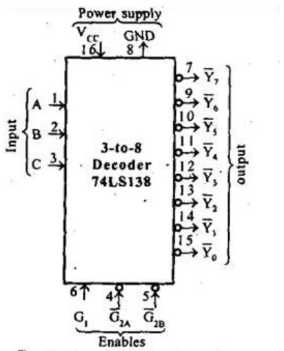
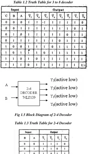
1.3.2Decoder
It is used to select the memory chip of processor during the execution of a program. No of IC's used for decoder is,
2-4 decoder (74LS139)
3-8 decoder (74LS138)
Table1.1 Number of Address Pins and Data Pins in Memory ICs
Table 1.2 Truth Table for 3 to 8 decoder
Fig 1.5 Block Diagram of 2-4 Decoder Table 1.3 Truth Table for 2-4 Decoder
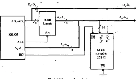
1.3.3 Example for Memory Interfacing
Consider a system in which the full memory space 64kb is utilized for EPROM memory. Interface the EPROM with 8085 processor.
2^n = 64 x 1000 bytes where n = address lines.
So, n = 16.
In this system the entire 16 address lines of the processor are connected to address input pins of memory IC in order to address the internal locations of memory.
The chip select (CS) pin of EPROM is permanently tied to logic low (i.e., tied to ground).
Since the processor is connected to EPROM, the active low RD pin is connected to active low output enable pin of EPROM.
The range of address for EPROM is 0000H to FFFFH.
Fig 1.6 Memory Interfacing
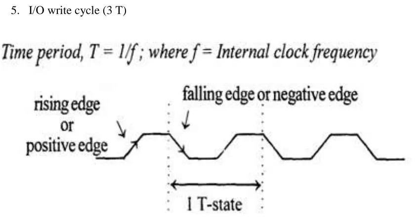
1.4 Timing Diagram
Timing Diagram is a graphical representation. It represents the execution time taken by each
instruction in a graphical format. The execution time is represented in T-states.
Instruction Cycle
Machine Cycle
The time required to access the memory or input/output devices is called machine cycle.
T-State
The machine cycle and instruction cycle takes multiple clock periods.
A portion of an operation carried out in one system clock period is called as T-state.
1.4.1 Machine cycles of 8085
The 8085 microprocessor has 5 (seven) basic machine cycles. They are 1. Opcode fetch cycle (4T)
2. Memory read cycle (3 T) 3. Memory write cycle (3 T) 4. I/O read cycle (3 T) 5. I/O write cycle (3 T)
Fig 1.7 Clock Signal
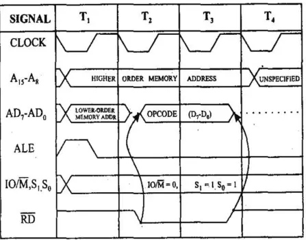
1.Opcode fetch machine cycle of 8085 :
The opcodes are stored in memory. So, the processor executes the opcode fetch machine cycle to fetch the opcode from memory.
Hence, every instruction starts with opcode fetch machine cycle.
The time taken by the processor to execute the opcode fetch cycle is 4T.
In this time, the first, 3 T-states are used for fetching the opcode from memory and the remaining T-states are used for internal operations by the processor.
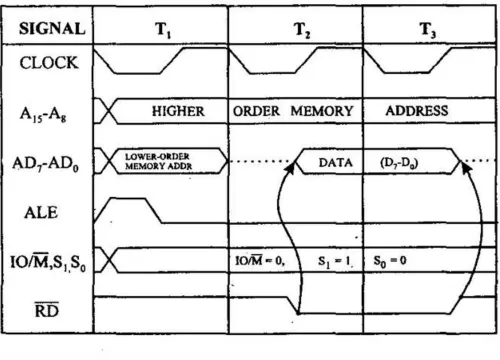
2.Memory Read Machine Cycle of 8085:
The memory read machine cycle is executed by the processor to read a data byte from memory.
The processor takes 3T states to execute this cycle.
The instructions which have more than one byte word size will use the machine cycle after the opcode fetch machine cycle.
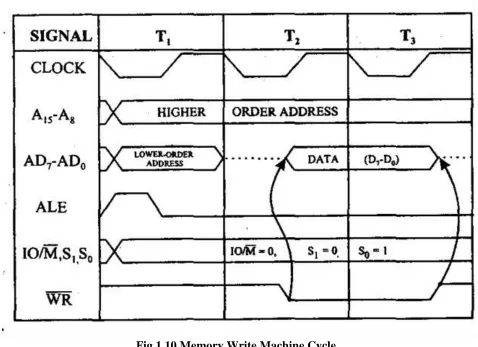
3.Memory Write Machine Cycle of 8085
The memory write machine cycle is executed by the processor to write a data byte in a memory location.
The processor takes, 3T states to execute this machine cycle.
Fig 1.10 Memory Write Machine Cycle
4. I/O Read Cycle of 8085
The I/O Read cycle is executed by the processor to read a data byte from I/O port or from the peripheral, which is I/O, mapped in the system.
The processor takes 3T states to execute this machine cycle.
Fig 1.11 I/O Read Cycle
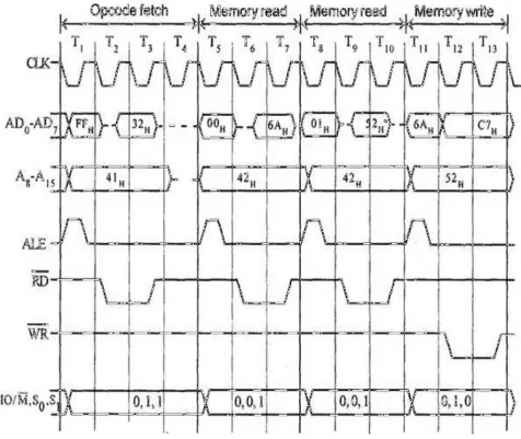
1.4.2 Timing diagram for STA 526AH
STA means Store Accumulator -The contents of the accumulator is stored in the specified address(526A).
The opcode of the STA instruction is said to be 32H. It is fetched from the memory 41FFH(see fig). - OF machine cycle
Then the lower order memory address is read(6A). - Memory Read Machine Cycle
Read the higher order memory address (52).- Memory Read Machine Cycle
The combination of both the addresses are considered and the content from accumulator is written in 526A. - Memory Write Machine Cycle
Fig 1.12 Timing Diagram for STA 526A H
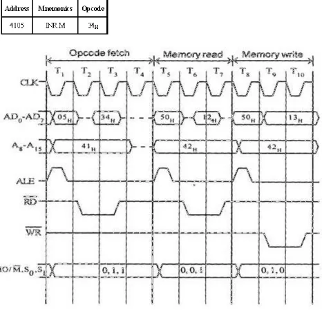
1.4.3 Timing diagram for INR M
Fetching the Opcode 34H from the memory 4105H. (OF cycle)
Let the memory address (M) be 4250H. (MR cycle -To read Memory address and data)
Let the content of that memory is 12H.
Fig 1.13 Timing Diagram for INR M
1.4.4
Timing diagram for MVI B, 43H.
Fetching the Opcode 06H from the memory 2000H. (OF machine cycle)
Fig 1.14 Timing Diagram for MVI B,43 H
1.5 Interrupts:
Mainly in the microprocessor based system the interrupts are used for data transfer between the peripheral and the microprocessor.
The processor will check the interrupts always at the 2nd T-state of last machine cycle.
If there is any interrupt it accept the interrupt and send the INTA (active low) signal to the peripheral.
The vectored address of particular interrupt is stored in program counter.
The processor executes an interrupt service routine (ISR) addressed in program counter.
It returned to main program by RET instruction.
1.5.1Types of Interrupts:
It supports two types of interrupts.
Hardware
Software
1.5.1.1 Software interrupts:
The software interrupts are program instructions. These instructions are inserted at desired locations in a program.
The 8085 has eight software interrupts from RST 0 to RST 7. The vector address for these interrupts can be calculated as follows.
Interrupt number * 8 = vector address
For RST 5,5 * 8 = 40 = 28H
Table 1.4 Vector addresses of all interrupts.
1.5.1.2 Hardware interrupts:
An external device initiates the hardware interrupts and placing an appropriate signal at the interrupt pin of the processor.
If the interrupt is accepted then the processor executes an interrupt service routine.
The 8085 has five hardware interrupts
(1) TRAP (2) RST 7.5 (3) RST 6.5 (4) RST 5.5 (5) INTR
(1)TRAP:
This interrupt is a non-maskable interrupt. It is unaffected by any mask or interrupt enable.
TRAP bas the highest priority and vectored interrupt.
In sudden power failure, it executes a ISR and send the data from main memory to backup memory.
The signal, which overrides the TRAP, is HOLD signal. (i.e., If the processor receives HOLD and TRAP at the same time then HOLD is recognized first and then TRAP is recognized).
There are two ways to clear TRAP interrupt.
1.By resetting microprocessor (External signal)
2.By giving a high TRAP ACKNOWLEDGE (Internal signal)
(2)RST 7.5:
The RST 7.5 interrupt is a maskable interrupt.
It has the second highest priority.
It is edge sensitive. ie. Input goes to high and no need to maintain high state until it recognized.
Maskable interrupt. It is disabled by,
1.DI instruction
2.System or processor reset. 3.After reorganization of interrupt.
Enabled by EI instruction.
(3)RST 6.5 and 5.5:
The RST 6.5 and RST 5.5 both are level triggered. . ie. Input goes to high and stay high until it recognized.
Maskable interrupt. It is disabled by,
3.After reorganization of interrupt.
Enabled by EI instruction.
The RST 6.5 has the third priority whereas RST 5.5 has the fourth priority.
(4)INTR:
INTR is a maskable interrupt. It is disabled by,
1.DI, SIM instruction 2.System or processor reset. 3.After reorganization of interrupt
Enabled by EI instruction.
Non- vectored interrupt. After receiving INTA (active low) signal, it has to supply the address of ISR.
It has lowest priority.
It is a level sensitive interrupts. ie. Input goes to high and it is necessary to maintain high state until it recognized.
The following sequence of events occurs when INTR signal goes high.
1. The 8085 checks the status of INTR signal during execution of each instruction.
2. If INTR signal is high, then 8085 complete its current instruction and sends active low interrupt acknowledge signal, if the interrupt is enabled.
4. On receiving the instruction, the 8085 save the address of next instruction on stack and execute received instruction.
SIM and RIM for interrupts:
The 8085 provide additional masking facility for RST 7.5, RST 6.5 and RST 5.5 using SIM instruction.
The status of these interrupts can be read by executing RIM instruction.
The masking or unmasking of RST 7.5, RST 6.5 and RST 5.5 interrupts can be
performed by moving an 8-bit data to accumulator and then executing SIM instruction.
The status of pending interrupts can be read from accumulator after executing RIM instruction.
When RIM instruction is executed an 8-bit data is loaded in accumulator, which can be interpreted as shown in fig.
Fig 1.16 Format of 8 bit data in Accumulator after executing RIM Instruction
1.6 Introduction to 8086 Microprocessor
1.6.1 Features:
1. Intel 8086 was launched in 1978. 2. It was the first 16-bit microprocessor.
3. This microprocessor had major improvement over the execution speed of 8085. 4. It is available as 40-pin Dual-Inline-Package (DIP).
5. It is available in three versions: a. 8086 (5 MHz)
1.6.2 Architecture of 8086 Microprocessor
Fig 1.17 Architecture of 8086
1.6.2.1 Bus Interface Unit (BIU):
The function of BIU is to
Fetch the instruction or data from memory.
Write the data to memory.
Write the data to the port.
Read data from the port.
1.6.2.2
Instruction Queue
1. To increase the execution speed, BIU fetches as many as six instruction bytes ahead to timefrom memory.
2. All six bytes are then held in first in first out 6 byte register called instruction queue.
3. Then all bytes have to be given to EU one by one.
EU, which improves the speed execution of the instruction.
1.6.2.3
Execution Unit (EU)
The functions of execution unit are
To tell BIU where to fetch the instructions or data from.
To decode the instructions.
To execute the instructions.
The EU contains the control circuitry to perform various internal operations. A decoder in EU decodes the instruction fetched memory to generate different internal or external control signals required to perform the operation. EU has 16-bit ALU, which can perform arithmetic and logical operations on 8-bit as well as 16-bit.
1.6.2.4 General Purpose Registers of 8086
These registers can be used as 8-bit registers individually or can be used as 16-bit in pair to have AX,BX, CX, and DX.
1. AX Register: AX register is also known as accumulator register that stores operands for arithmetic operation like divided, rotate.
2. BX Register: This register is mainly used as a base register. It holds the starting base location of a memory region within a data segment.
3. CX Register: It is defined as a counter. It is primarily used in loop instruction to store loop counter.
1.6.2.5 Segment Registers
Additional registers called segment registers generate memory address when combined with other in the microprocessor. In 8086 microprocessor, memory is divided into 4 segments as follow:
Fig 1.18 Memory Segments of 8086
1. Code Segment (CS): The CS register is used for addressing a memory location in the Code Segment of the memory, where the executable program is stored.
2. Data Segment (DS): The DS contains most data used by program. Data are accessed in the Data Segment by an offset address or the content of other register that holds the offset
address.
3. Stack Segment (SS): SS defined the area of memory used for the stack.
4. Extra Segment (ES): ES is additional data segment that is used by some of the string to hold the destination data.
Fig 1.19 Flag Register of 8086
Flags Register determines the current state of the processor. They are modified automatically by CPU after mathematical operations, this allows to determine the type of the result, and to determine conditions to transfer control to other parts of the program. 8086 has 9 flags and they are divided into two categories:
1. Conditional Flags
2. Control Flags
(1) Conditional Flags
Conditional flags represent result of last arithmetic or logical instruction executed. Conditional flags are as follows:
Carry Flag (CF)
This flag indicates an overflow condition for unsigned integer arithmetic. It is also used in multiple-precision arithmetic.
Auxiliary Flag (AF):
If an operation performed in ALU generates a carry/barrow from lower nibble (i.e. D0 D3) to upper nibble (i.e. D4 – D7), the AF flag is set i.e. carry given by D3 bit to D4 is AF flag. This is not a general-purpose flag, it is used internally by the processor to perform Binary to BCD conversion.
Parity Flag (PF):
This flag is used to indicate the parity of result. If lower order 8-bits of the
result contains even number of 1‟s, the Parity Flag is set and for odd number of 1‟s, the Parity Flag is reset.
Zero Flag (ZF):
Sign Flag (SF):
In sign magnitude format the sign of number is indicated by MSB bit. If the result of operation is negative, sign flag is set.
Overflow Flag (OF):
It occurs when signed numbers are added or subtracted. An OF indicates that the result has exceeded the capacity of machine.
Control Flags
Control flags are set or reset deliberately to control the operations of the execution unit. Control flags are as follows:
1. Trap Flag (TP):
a. It is used for single step control.
b. It allows user to execute one instruction of a program at a time for debugging.
c. When trap flag is set, program can be run in single step mode.
2. Interrupt Flag (IF):
a. It is an interrupt enable/disable flag.
b. If it is set, the maskable interrupt of 8086 is enabled and if it is reset, the interrupt is disabled.
c. It can be set by executing instruction sit and can be cleared by executing CLI instruction.
3. Direction Flag (DF):
a. It is used in string operation.
b. If it is set, string bytes are accessed from higher memory address to lower memory address.
1.6.3 8086-Minimum mode of operation
Fig 1.20 Minimum mode of 8086
1.6.3.1Minimum Mode Interface
Address/Data bus: 20 bits vs 8 bits multiplexed
Status signals: A16-A19 multiplexed with status signals S3-S6 respectively
– S3 and S4 together form a 2 bit binary code that identifies which of the internal segment registers was used to generate the physical address that was output on the address bus during the current bus cycle.
– S5 is the logic level of the internal interrupt enable flag, s6 is always logic 0.
– Address Latch Enable (ALE) is a pulse to logic 1 that signals external circuitry when a valid address is on the bus. This address can be latched in external circuitry on the 1-to-0 edge of the pulse at ALE.
– IO/M line: memory or I/O transfer is selected (complement for 8086) – DT/R line: direction of data is selected
– SSO (System Status Output) line: =1 when data is read from memory and =0 when code is read from memory (only for 8088)
– BHE (Bank High Enable) line : =0 for most significant byte of data for 8086 and also carries S7
– RD line: =0 when a read cycle is in progress – WR line: =0 when a write cyle is in progress
– DEN line: (Data enable) Enables the external devices to supply data to the processor.
– Ready line: can be used to insert waitstates into the bus cycle so that it is extended by a number of clock periods
Interrupt signals:
– INTR (Interrupt request) :=1 shows there is a service request, sampled at the final clock cycle of each instruction acquisition cycle.
– INTA : Processor responds with two pulses going to 0 when it services the interrupt and waits for the interrupt service number after the second pulse.
– TEST: Processor suspends operation when =1. Resumes operation when=0. Used to syncronize the processor to external events.
– NMI (Nonmaskable interrupt) : A leading edge transition causes the processor go to the interrupt routine after the current instruction is executed.
– RESET : =0 Starts the reset sequence.
1.6.4 Maximum Mode Interface
• For multiprocessor environment
• 8288 Bus Controller is used for bus control
• Instead
– MRDC¯ (memory read command) – MWRT¯ (memory write command)
– AMWC¯ (advanced memory write command) – IORC¯ (I/O read command)
– IOWC¯ (I/O write command)
– AIOWC¯ (Advanced I/O write command) – INTA¯ (interrupt acknowledge)
Fig 1.22Block and Pin Diagram of 8288 Bus controller
– The signals shown above are produced by 8288 depending on the state of S0, S1 and S2. • DEN, DT/R¯ and ALE signals are the same as minimum-mode systems
• LOCK¯: when =0, prevents other processors from using the bus
• QS0 and QS1 (queue status signals) : informs about the status of the queue
• RQ¯/GT ¯0 and RQ¯/GT ¯1 are used instead of HOLD and HLDA lines in a multiprocessor environment as request/grant lines.
1.7I/O Ports
There are two methods in which I/O devices can be connected to the Microprocessor.
(i)Memory mapped I/O
(ii)I/O mapped I/O
(i) Memory mapped I/O
address wioll also get selected.so we have to use separate address for memory and separate address for I/O device.
(ii)I/O mapped I/O
Here we hve the IO/M signal.So we can select either the memory or I/O device for read and write operation.
1.8 Data Transfer Concepts
(i)Parallel data transfer
(ii)Serial data transfer
(i)Parallel Data transfer
(a)Programmed I/O
(b) Interrupt I/O
(C) DMA
(a)Programmed I/O
Here the processor has to check whether the I/O device is ready or not through the Ready signal of the I/O device.If the ready signal is high then it will send the data to the I/O device.Otherwise it will continuously check theReady signal.The processor is busy in checking the Ready signal.The draw back is wastage of time.
(b) Interrupt I/O
In this method the I/O device will interrupt the Processor through the INTR signal to indicate to the processor that it is ready to accept the next data.Then the processor will send the INTA signal.Then the processor stops its normal execution and start transferring the data to the I/O device.
(c)DMA
(ii)Serial data Transfer
Some of the external I/0 devices receive only the serial data.Normally serial communication is used in the Multi Processor environment.8051 has two pins for serial communication.
(1)SID- Serial Input data.
(2)SOD-Serial Output data.
UNIT II
PROGRAMMING OF 8085 MICROPROCESSOR
2.1 Instruction Format
An instruction is a command to the microprocessor to perform a given task on a specified data. Each instruction has two parts: one is task to be performed, called the
operation code (opcode), and the second is the data to be operated on, called the
operand. The operand (or data) can be specified in various ways. It may include 8-bit (or 16-bit ) data, an internal register, a memory location, or 8-bit (or 16-bit) address. In some instructions, the operand is implicit.
Instruction word size
The 8085 instruction set is classified into the following three groups according to word size:
1. One-word or 1-byte instructions
2. Two-word or 2-byte instructions
3. Three-word or 3-byte instructions
In the 8085, "byte" and "word" are synonymous because it is an 8-bit microprocessor. However, instructions are commonly referred to in terms of bytes rather than words.
2.1.1 One-Byte Instructions
Table 2.1 Example for 1 byte Instruction
These instructions are 1-byte instructions performing three different tasks. In the first instruction, both operand registers are specified. In the second instruction, the operand B is specified and the accumulator is assumed. Similarly, in the third instruction, the accumulator is assumed to be the implicit operand. These instructions are stored in 8- bit binary format in memory; each requires one memory location.
MOV rd, rs
rd <-- rs copies contents of rs into rd.
Coded as 01 ddd sss where ddd is a code for one of the 7 general registers which is the destination of the data, sss is the code of the source register.
Example: MOV A,B
Coded as 01111000 = 78H = 170 octal (octal was used extensively in instruction design of such processors).
ADD r
A <-- A + r
2.1.2 Two-Byte Instructions
Table 2.2 Example for 2 byte Instruction
The instruction would require two memory locations to store in memory.
MVI r,data
r <-- data
Example: MVI A,30H coded as 3EH 30H as two contiguous bytes. This is an example of immediate addressing.
ADI data
A <-- A + data OUT port 0011 1110
DATA
where port is an 8-bit device address. (Port) <-- A. Since the byte is not the data but points directly to where it is located this is called direct addressing.
2.1.3 Three-Byte Instructions
In a three-byte instruction, the first byte specifies the opcode, and the following two bytes specify the 16-bit address. Note that the second byte is the low-order address
Table 3.3 Example for 3 byte Instruction
This instruction would require three memory locations to store in memory. Three byte instructions - opcode + data byte + data byte
LXI rp, data16
rp is one of the pairs of registers BC, DE, HL used as 16-bit registers. The two data bytes are 16-bit data in L H order of significance.
rp <-- data16
LXI H,0520H coded as 21H 20H 50H in three bytes. This is also immediate addressing.
LDA addr
A <-- (addr) Addr is a 16-bit address in L H order. Example: LDA 2134H coded as
3AH 34H 21H. This is also an example of direct addressing.
2.2 The 8085 Addressing Modes
The instructions MOV B, A or MVI A, 82H are to copy data from a source into a destination. In these instructions the source can be a register, an input port, or an 8-bit number (00H to FFH). Similarly, a destination can be a register or an output port. The sources and destination are operands. The various formats for specifying operands are called the ADDRESSING MODES. For 8085, they are:
1. Immediate addressing. 2. Register addressing. 3. Direct addressing. 4. Indirect addressing.
(1)Immediate addressing
Example: MVI R,data
(2)Register addressing
Data is provided through the registers.
Example: MOV Rd, Rs
(3)Direct addressing
Used to accept data from outside devices to store in the accumulator or send the data stored in the accumulator to the outside device. Accept the data from the port 00H and store them into the accumulator or Send the data from the accumulator to the port 01H.
Example: IN 00H or OUT 01H
(4)Indirect Addressing
This means that the Effective Address is calculated by the processor. And the
contents of the address (and the one following) is used to form a second address. The second address is where the data is stored. Note that this requires several memory accesses; two accesses to retrieve the 16-bit address and a further access (or accesses) to retrieve the data which is to be loaded into the register.
2.3 Instruction Set Classification
An instruction is a binary pattern designed inside a microprocessor to perform a specific function. The entire group of instructions, called the instruction set,
determines what functions the microprocessor can perform. These instructions can be classified into the following five functional categories: data transfer (copy)
operations, arithmetic operations, logical operations, branching operations, and machine-control operations.
2.3.1 Data Transfer Croup
The data transfer instructions move data between registers or between memory and registers.
MOV Move
MVI Move Immediate
SHLD Store H & L Registers Directly in Memory
An 'X' in the name of a data transfer instruction implies that it deals with a register pair (16-bits);
LXI Load Register Pair with Immediate data
LDAX Load Accumulator from Address in Register Pair STAX Store Accumulator in Address in Register Pair XCHG Exchange H & L with D & E
XTHL Exchange Top of Stack with H & L
2.3.2 Arithmetic Group
The arithmetic instructions add, subtract, increment, or decrement data in registers or memory.
ADD Add to Accumulator
ADI Add Immediate Data to Accumulator ADC Add to Accumulator Using Carry Flag
ACI Add Immediate data to Accumulator Using Carry
SUB Subtract from Accumulator
SUI Subtract Immediate Data from Accumulator
SBB Subtract from Accumulator Using Borrow (Carry) Flag
SBI Subtract Immediate from Accumulator Using Borrow (Carry) Flag INR Increment Specified Byte by One
DCR Decrement Specified Byte by One INX Increment Register Pair by One DCX Decrement Register Pair by One
DAD Double Register Add; Add Content of Register Pair to H & L Register Pair
2.3.3 Logical Group
This group performs logical (Boolean) operations on data in registers and memory and on condition flags.
The logical AND, OR, and Exclusive OR instructions enable you to set specific bits in the accumulator ON or OFF.
ANA Logical AND with Accumulator
ANI Logical AND with Accumulator Using Immediate Data
ORA Logical OR with Accumulator
OR Logical OR with Accumulator Using Immediate Data XRA Exclusive Logical OR with Accumulator
XRI Exclusive OR Using Immediate Data
The Compare instructions compare the content of an 8-bit value with the contents of the accumulator;
CMP Compare
CPI Compare Using Immediate Data
The rotate instructions shift the contents of the accumulator one bit position to the left or right:
RLC Rotate Accumulator Left
RRC Rotate Accumulator Right
RAL Rotate Left Through Carry RAR Rotate Right Through Carry
Complement and carry flag instructions:
CMA Complement Accumulator
CMC Complement Carry Flag
STC Set Carry Flag
2.3.4 Branch Group
The branching instructions alter normal sequential program flow, either unconditionally or conditionally. The unconditional branching instructions are as follows:
JMP Jump
CALL Call
RET Return
NZ Not Zero (Z = 0)
Z Zero (Z = 1)
NC No Carry (C = 0)
C Carry (C = 1)
PO Parity Odd (P = 0)
PE Parity Even (P = 1)
P Plus (S = 0)
M Minus (S = 1)
Thus, the conditional branching instructions are specified as follows:
Jumps Calls Returns
C CC RC (Carry)
INC CNC RNC (No Carry)
JZ CZ RZ (Zero)
JNZ CNZ RNZ (Not Zero)
JP CP RP (Plus)
JM CM RM (Minus)
JPE CPE RPE (Parity Even)
JP0 CPO RPO (Parity Odd)
Two other instructions can affect a branch by replacing the contents or the program counter:
PCHL Move H & L to Program Counter RST Special Restart Instruction Used
with Interrupts
2.3.5 Stack Instructions
The following instructions affect the Stack and/or Stack Pointer
POP Pop Two Bytes of Data off the Stack XTHL Exchange Top of Stack with H & L SPHL Move content of H & L to Stack Pointer
2.3.6 I/0 instructions
IN Initiate Input Operation OUT Initiate Output Operation
2.3.7 Machine Control instructions
EI Enable Interrupt System
DI Disable Interrupt System
HLT Halt
NOP No Operation
2.4 Sample Program
(1)Write an assembly program to add two numbers Program MVI D, 8BH
MVI C, 6FH MOV A, C 1100 0011 1000 0101 0010 0000 ADD D OUT PORT1 HLT
(2)Write an assembly program to multiply a number by 8 Program MVI A, 30H
RRC RRC RRC
OUT PORT1 HLT
(3)Write an assembly program to find greatest between two numbers Program MVI B, 30H
HLT
EQU: MVI A, 01H OUT PORT1 HLT
GRT: MOV A, C OUT PORT1 HLT
2.5 Programming using Loop structure with Counting and Indexing
(i) 16 bit Multiplication
ADDRESS LABEL MNEMONICS OPCODE
MOV H,B SHLD 4206 HLT
(ii)Finding the maximum number in the given array
ADDRESS LABEL MNEMONICS OPCODE
START
L2 L3
L1
LDA 4500 MOV C, A LXI H, 4501 MOV A, M DCR C INX H JZ L1 CMP M JC L2 JMP L3 STA 4520 HLT
(iii) To sort the array of data in ascending order
START L3
L2
L1
MVI B, 00 LXI H, 4200 MOV C, M DCR C INX H MOV A, M INX H CMP M JC L1 MOV D, M MOV M, A DCX H MOV M, D INX H MVI B, 01 DCR C JNZ L2 DCR B JZ L3 HLT
2.6 Programming using subroutine Instructions
ADDRESS LABEL MNEMONICS START DELAY L2 L1 MVI A,00H OUT C8 CALL DELAY
MVI A,FF
OUT C8
CALL DELAY
JMP START
MVI B,05H
MVI C,FF
DCR C JNZ L1 DCR B JNL L2
2.7 Programming using Look up table
ADDRESS LABEL MNEMONICS OPCODE
START
L2
MVI B,08
MVI A,00(DISPLAY MODE SETUP)
OUT C2
MVI A,CC(CLEAR DISPLAY) OUT C2
MVI A,90(WRITE DISPLAY RAM)
OUT C2
MVI A, FF(CLEAR DISPLAY RAM)
OUT C0 DCR B JNZ L1 IN C2 ANI 07 JZ L2
MVI A, 40(SET TO READ FIFO RAM)
MOV L, A MVI H, 42 MOV A, M OUT C0 JMP L2
LOOKUP TABLE
4200 0C 9F 4A 0B
4204 99 29 28 8F
4208 08 09 88 38
420C 6C 1A 68 E8
UNIT III
PERIPHERAL INTERFACING
3.1 Programmable peripheral interface(8255)
3.1.1 Architecture of 8255
port C lower can be used in combination as an 8-bit port C. Both the port C are assigned the same address. Thus one may have either three 8-bit I/O ports or two 8-bit and two 4-bit ports from 8255. All of these ports can function independently either as input or as output ports. This can be achieved by programming the bits of an internal register of 8255 called as control word register ( CWR ). This buffer receives or transmits data upon the execution of input or output instructions by the microprocessor. The control words or status information is also transferred through the buffer.
Fig 3.1 8255 Architecture
Fig 3.2 Pin Diagram of 8255
The signal description of 8255 are briefly presented as follows :
• PA7-PA0: These are eight port A lines that acts as either latched output or buffered input lines depending upon the control word loaded into the control word register.
• PC7-PC4 : Upper nibble of port C lines. They may act as either output latches or input buffers lines.This port also can be used for generation of handshake lines in mode 1 or mode 2.
• PC3-PC0 : These are the lower port C lines, other details are the same as PC7-PC4 lines. • PB0-PB7 : These are the eight port B lines which are used as latched output lines or buffered input lines in the same way as port A.
• RD : This is the input line driven by the microprocessor and should be low to indicate read operation to 8255.
• WR : This is an input line driven by the microprocessor. A low on this line indicates write operation.
• A1-A0 : These are the address input lines and are driven by the microprocessor. These lines A1-A0 with RD, WR and CS from the following operations for 8255. These address
lines are used for addressing any one of the four registers,i.e. three ports and a control word register as given in table below.
• In case of 8086 systems, if the 8255 is to be interfaced with lower order data bus, the A0 and A1 pins of 8255 are connected with A1 and A2 respectively.
D0-D7 : These are the data bus lines those carry data or control word to/from the microprocessor.
• RESET : A logic high on this line clears the control word register of 8255. All ports are set as input ports by default after reset.
3.1.3 Operational Modes of 8255
There are two main operational modes of 8255:
1. Input/output mode 2. Bit set/reset mode
3.1.3.1 Input/Output Mode
There are three types of the input/output mode. They are as follows:
Mode 0
In this mode, the ports can be used for simple input/output operations without handshaking. If both port A and B are initialized in mode 0, the two halves of port C can be either used together as an additional 8-bit port, or they can be used as individual 4-bit ports. Since the two halves of port C are independent, they may be used such that one-half is initialized as an input port while the other half is initialized as an output port. The input output features in mode 0 are as follows: 1. O/p are latched. 2. I/p are buffered not latched. 3. Port do not have handshake or interrupt capability.
When we wish to use port A or port B for handshake (strobed) input or output operation, we initialise that port in mode 1 (port A and port B can be initilalised to operate in different modes,ie, for eg, port A can operate in mode 0 and port B in mode 1). Some of the pins of port C function as handshake lines.
For port B in this mode (irrespective of whether is acting as an input port or output port), PC0, PC1 and PC2 pins function as handshake lines.
If port A is initialised as mode 1 input port, then, PC3, PC4 and PC5 function as handshake signals. Pins PC6 and PC7 are available for use as input/output lines.
The mode 1 which supports handshaking has following features: 1. Two ports i.e. port A and B can be use as 8-bit i/o port. 2. Each port uses three lines of port c as handshake signal and remaining two signals can be function as i/o port. 3. interrupt logic is supported. 4. Input and Output data are latched.
Mode 2
Only group A can be initialised in this mode. Port A can be used for bidirectional handshake data transfer. This means that data can be input or output on the same eight lines (PA0 - PA7). Pins PC3 - PC7 are used as handshake lines for port A. The remaining pins of port C (PC0 - PC2) can be used as input/output lines if group B is initialised in mode 0. In this mode, the 8255 may be used to extend the system bus to a slave microprocessor or to transfer data bytes to and from a floppy disk controller.
3.1.3.2 Bit Set/Reset (BSR) mode
3.1.4 Control Word Format
3.1.4.1 Input/output mode format
D7 D6 D5 D4 D3 D2 D1 D0
1 (1=I/O) GA mode select PA PCU GB mode select PB PCL
Fig 3.3 Control Word format for Input/Output Mode
Control Word format in input/output mode
The figure shows the control word format in the input/output mode. This mode is selected by making D7 = '1' .
D0, D1, D3, D4 are for lower port C, port B, upper port C and port A respectively. When D0 or D1 or D3 or D4 are "SET", the corresponding ports act as input ports. For eg, if D0 = D4 = '1', then lower port C and port A act as input ports. If these bits are "RESET", then the corresponding ports act as output ports. For eg, if D1 = D3 = '0', then port B and upper port C act as output ports.
D2 is used for mode selection for group B (Port B and Lower Port C). When D2 = '0', mode 0 is selected and when D2 = '1', mode 1 is selected.
D5, D6 are used for mode selection for group A (Upper Port C and Port A). The format is as follows:
D6 D5 mode 0 0 0 0 1 1 1 x 2
3.1.4.2 BSR mode format
D7 D6 D5 D4 D3 D2 D1 D0
0 (0=BSR) X X X B2 B1 B0 S/R (1=S,0=R)
Bit select: (Taking Don't care's as 0)
B2 B1 B0 PC bit Control word (Set) Control word (reset)
0 0 0 0 0000 0001 = 01h 0000 0000 = 00h
0 0 1 1 0000 0011 = 03h 0000 0010 = 02h
0 1 0 2 0000 0101 = 05h 0000 0100 = 04h
0 1 1 3 0000 0111 = 07h 0000 0110 = 06h
1 0 0 4 0000 1001 = 09h 0000 1000 = 08h
1 0 1 5 0000 1011 = 0Bh 0000 1010 = 0Ah
1 1 0 6 0000 1101 = 0Dh 0000 1100 = 0Ch
1 1 1 7 0000 1111 = 0Fh 0000 1110 = 0Eh
Fig 3.4 Control Word format in BSR mode
The figure shows the control word format in BSR mode. This mode is selected by making
D7='0'.
D0 is used for bit set/reset. When D0= '1', the port C bit selected (selection of a port C bit is shown in the next point) is SET, when D0 = '0', the port C bit is RESET.
D1, D2, D3 are used to select a particular port C bit whose value may be altered using D0 bit as mentioned above. The selection of the port C bits are done as follows:
D3 D2 D1 bit/pin of port C selected 0 0 0 PC0
0 0 1 PC1 0 1 0 PC2 0 1 1 PC3 1 0 0 PC4 1 0 1 PC5 1 1 0 PC6 1 1 1 PC7
D4, D5, D6 are not used.
3.2Programmable Interrupt Controller(8259)
3.2.1 Features
8 levels of interrupts.
Can be cascaded in master-slave configuration to handle 64 levels of interrupts.
Internal priority resolver.
Fixed priority mode and rotating priority mode.
Individually maskable interrupts.
Modes and masks can be changed dynamically.
Accepts IRQ, determines priority, checks whether incoming priority > current level being serviced, issues interrupt signal.
In 8085 mode, provides 3 byte CALL instruction. In 8086 mode, provides 8 bit vector number.
Polled and vectored mode.
Starting address of ISR or vector number is programmable.
No clock required.
Fig 3.5 Pin Diagram of 8259
Table 3.1 Pin Description of 8259
3.2.3 Block diagram
D0-D7 Bi-directional, tristated, buffered data lines. Connected to data bus directly or through buffers
RD-bar Active low read control
WR-bar Active low write control
A0 Address input line, used to select control register
CS-bar Active low chip select
CAS0-2
Bi-directional, 3 bit cascade lines. In master mode, PIC places slave ID no. on these lines. In slave mode, the PIC reads slave ID no. from master on these lines. It may be regarded as slave-select.
SP-bar / EN-bar
Slave program / enable. In non-buffered mode, it is SP-bar input, used to distinguish master/slave PIC. In buffered mode, it is output line used to enable buffers
INT Interrupt line, connected to INTR of microprocessor
INTA-bar Interrupt ack, received active low from microprocessor
Fig 3.6 Block Diagram of 8259
ICW1 (Initialisation Command Word One) A0
0
D7 D6 D5 D4 D3 D2 D1 D0
A7 A6 A5 1 LTIM ADI SNGL IC4
D0: IC4: 0=no ICW4, 1=ICW4 required D1: SNGL: 1=Single PIC, 0=Cascaded PIC
D2: ADI: Address interval. Used only in 8085, not 8086. 1=ISR's are 4 bytes apart (0200, 0204, etc) 0=ISR's are 8 byte apart (0200, 0208, etc)
D3: LTIM: level triggered interrupt mode: 1=All IR lines level triggered. 0=edge triggered D4-D7: A5-A7: 8085 only. ISR address lower byte segment. The lower byte is
A7 A6 A5 A4 A3 A2 A1 A0
of which A7, A6, A5 are provided by D7-D5 of ICW1 (if ADI=1), or A7, A6 are provided if ADI=0. A4-A0 (or A5-A0) are set by 8259 itself:
ADI=1 (spacing 4 bytes)
IRQ A7 A6 A5 A4 A3 A2 A1 A0
IR0 A7 A6 A5 0 0 0 0 0
IR1 A7 A6 A5 0 0 1 0 0
IR2 A7 A6 A5 0 1 0 0 0
IR3 A7 A6 A5 0 1 1 0 0
IR4 A7 A6 A5 1 0 0 0 0
IR5 A7 A6 A5 1 0 1 0 0
IR6 A7 A6 A5 1 1 1 0 0
IR7 A7 A6 A5 1 1 1 0 0
ADI=0 (spacing 8 bytes)
IRQ A7 A6 A5 A4 A3 A2 A1 A0
IR0 A7 A6 0 0 0 0 0 0
IR1 A7 A6 0 0 1 0 0 0
IR2 A7 A6 0 1 0 0 0 0
IR3 A7 A6 0 1 1 0 0 0
IR4 A7 A6 1 0 0 0 0 0
IR5 A7 A6 1 0 1 0 0 0
IR6 A7 A6 1 1 0 0 0 0
ICW2 (Initialisation Command Word Two)
Higher byte of ISR address (8085), or 8 bit vector address (8086).
A0 1
D7 D6 D5 D4 D3 D2 D1 D0
A15 A14 A13 A12 A11 A10 A9 A8
ICW3 (Initialisation Command Word Three)
A0 1
D7 D6 D5 D4 D3 D2 D1 D0
Master S7 S6 S5 S4 S3 S2 S1 S0
Slave 0 0 0 0 0 ID3 ID2 ID1
Master mode: 1 indicates slave is present on that interrupt, 0 indicates direct interrupt
Slave mode: ID3-ID2-ID1 is the slave ID number. Slave 4 on IR4 has ICW3=04h (0000 0100)
ICW4 (Initialisation Command Word Four)
A0 1
D7 D6 D5 D4 D3 D2 D1 D0
0 0 0 SFNM BUF M/S AEOI Mode
SFNM: 1=Special Fully Nested Mode, 0=FNM
M/S: 1=Master, 0=Slave
AEOI: 1=Auto End of Interrupt, 0=Normal
Mode: 0=8085, 1=8086
OCW1 (Operational Command Word One)
A0 1
D7 D6 D5 D4 D3 D2 D1 D0
M7 M6 M5 M4 M3 M2 M1 M0
IRn is masked by setting Mn to 1; mask cleared by setting Mn to 0 (n=0..7)
OCW2 (Operational Command Word Two)
1 R SL EOI 0 0 L3 L2 L1
R SL EOI Action
EOI
0 0 1 Non specific EOI (L3L2L1=000)
0 1 1 Specific EOI command (Interrupt to clear given by L3L2L1)
Auto rotation of priorities (L3L2L1=000)
1 0 1 Rotate priorities on non-specific EOI
1 0 0 Rotate priorities in auto EOI mode set
0 0 0 Rotate priorities in auto EOI mode clear
Specific rotation of priorities (Lowest priority ISR=L3L2L1)
1 1 1 Rotate priority on specific EOI command (resets current ISR bit)
1 1 0 Set priority (does not reset current ISR bit)
0 1 0 No operation
OCW3 (Operational Command Word Three)
A0 1
D7 D6 D5 D4 D3 D2 D1 D0
D7 ESMM SMM 0 1 MODE RIR RIS
ESMM SMM Effect
0 X No effect
1 0 Reset special mask
1 1 Set special mask
3.3 8251 UNIVERSAL SYNCHRONOUS ASYNCHRONOUS RECEIVER
TRANSMITTER (USART)
The 8251 is a USART (Universal Synchronous Asynchronous Receiver Transmitter) for serial data communication. As a peripheral device of a microcomputer system, the 8251receives parallel data from the CPU and transmits serial data after conversion. This device also receives serial data from the outside and transmits parallel data to the CPU after conversion.
Fig 3.7 Block diagram of the 8251 USART (Universal Synchronous Asynchronous Receiver Transmitter)
3.3.2 Control Words
1) Mode Instruction
Mode instruction is used for setting the function of the 8251. Mode instruction will be in "wait for write" at either internal reset or external reset. That is, the writing of a control word after resetting will be recognized as a "mode instruction."
Items set by mode instruction are as follows:
• Synchronous/asynchronous mode
• Stop bit length (asynchronous mode)
• Character length
• Parity bit
• Baud rate factor (asynchronous mode)
• Internal/external synchronization (synchronous mode)
• Number of synchronous characters (Synchronous mode)
Fig 3.8 Bit Configuration of Mode Instruction(Asynchronous)
Fig 3.9 Bit Configuration of Mode Instruction(synchronous)
2) Command
Command is used for setting the operation of the 8251. It is possible to write a command whenever necessary after writing a mode instruction and sync characters.
Items to be set by command are as follows:
• Transmit Enable/Disable
• DTR, RTS Output of data.
• Resetting of error flag.
• Sending to break characters
• Internal resetting
• Hunt mode (synchronous mode)
3.3.3 Status Word
It is possible to see the internal status of the 8251 by reading a status word.
Fig 3.11 Bit Configuration of Status Word
3.4 Programmable Keyboard/Display Interface - 8279
3.4.1 Pinout Definition 8279
.Fig 3.12 Pin Diagram of 8279
A0: Selects data (0) or control/status (1) for reads and writes between micro and 8279.
BD: Output that blanks the displays.
CLK: Used internally for timing. Max is 3 MHz.
CN/ST: Control/strobe, connected to the control key on the keyboard
CS: Chip select that enables programming, reading the keyboard, etc.
DB7-DB0: Consists of bidirectional pins that connect to data bus on micro.
IRQ: Interrupt request, becomes 1 when a key is pressed, data is available.
OUT A3-A0/B3-B0: Outputs that sends data to the most significant/least significant nibble of display.
RD(WR): Connects to micro's IORC or RD signal, reads data/status registers.
RESET: Connects to system RESET.
RL7-RL0: Return lines are inputs used to sense key depression in the keyboard matrix.
SL3-SL0: Scan line outputs scan both the keyboard and displays.
3.4.2 Block Diagram of 8279
Fig 3.13 Block Diagram of 8279 Display section:
The display section has eight output lines divided into two groups A0-A3 and B0-B3.
The output lines can be used either as a single group of eight lines or as two groups of four lines, in conjunction with the scan lines for a multiplexed display.
The output lines are connected to the anodes through driver transistor in case of common cathode 7-segment LEDs.
The cathodes are connected to scan lines through driver transistors. The display can be blanked by BD (low) line.
Scan section:
The scan section has a scan counter and four scan lines, SL0 to SL3.
In decoded scan mode, the output of scan lines will be similar to a 2-to-4 decoder. In encoded scan mode, the output of scan lines will be binary count, and so an
external decoder should be used to convert the binary count to decoded output. The scan lines are common for keyboard and display.
The scan lines are used to form the rows of a matrix keyboard and also connected to digit drivers of a multiplexed display, to turn ON/OFF.
CPU interface section:
The CPU interface section takes care of data transfer between 8279 and the processor.
This section has eight bidirectional data lines DB0 to DB7 for data transfer between 8279 and CPU.
It requires two internal address A =0 for selecting data buffer and A = 1 for selecting control register of8279.
The control signals WR (low), RD (low), CS (low) and A0 are used for read/write to 8279.
It has an interrupt request line IRQ, for interrupt driven data transfer with processor.
The 8279 require an internal clock frequency of 100 kHz. This can be obtained by dividing the input clock by an internal prescaler.
3.4.2 Keyboard Interface of 8279
The keyboard matrix can be any size from 2x2 to 8x8.Pins SL2-SL0 sequentially scan each column through a counting operation.The 74LS138 drives 0's on one line at a time.The 8279 scans RL pins synchronously with the scan.RL pins incorporate internal pull-ups, no need for external resistor pull-ups.The 8279 must be programmed first.
First three bits given below select one of 8 control registers (opcode).
000DDMMM
Mode set:Opcode 000. DD sets displays mode. MMM sets keyboard mode. DD field selects either:
8- or 16-digit display
Whether new data are entered to the rightmost or leftmost display position.
Encoded:SL outputs are active-high, follow binary bit pattern 0-7 or 0-15.
Decoded:SL outputs are active-low (only one low at any time). Pattern output: 1110, 1101, 1011, 0111.
Strobed:An active high pulse on the CN/ST input pin strobes data from the RL pins into an internal FIFO for reading by micro later.
Fig 3.13 Keyboard Interface of 8279
3.5 ADC Interfacing with 8085 Microprocessor
3.5.1 Features
The ADC0809 is an 8-bit successive approximation type ADC with inbuilt 8-channel multiplexer.
The ADC0809 is suitable for interface with 8086 microprocessor.
The ADC0809 is available as a 28 pin IC in DIP (Dual Inline Package).
The ADC0809 has a total unadjusted error of ±1 LSD (Least Significant Digit).
The ADC0808 is also same as ADC0809 except the error. The total unadjusted error in ADC0808 is ± 1/2 LSD.
3.5.2 Block Diagram of ADC 0809
Fig 3.16 Block Diagram of ADC 0809
The successive approximation register (SAR) performs eight iterations to determine the digital code for input value. The SAR is reset on the positive edge of START pulse and start the conversion process on the falling edge of START pulse. A conversion process will be interrupted on receipt of new START pulse. The End-Of-Conversion (EOC) will go low between 0 and 8 clock pulses after the positive edge of START pulse. The ADC can be used in continuous conversion mode by tying the EOC output to START input. In this mode an external START pulse should be applied whenever power is switched ON.
Then it converts AC signal to DC signal. This technique limits the drift component of the amplifier, because the drift is a DC component and it is not amplified/passed by the AC amp1ifier. This makes the ADC extremely insensitive to temperature, long term drift and input offset errors. In ADC conversion process the input analog value is quantized and each quantized analog value will have a unique binary equivalent. The quantization step in ADC0809/ADC0808 is given by,
PROGRAM
ADDRESS MNEMONICS OPCODE DESCRIPTION
MVI A,10 OUT 0C8 H MVI A,18 OUT 0C8 H HLT
Channel 0 select ALE Low
3.6 DAC Interfacing with 8085 Microprocessor
3.6.1 DAC 0800 Features
To convert the digital signal to analog signal a Digital-to-Analog Converter (DAC) has to be employed.
The DAC will accept a digital (binary) input and convert to analog voltage or current.
Every DAC will have "n" input lines and an analog output.
The DAC require a reference analog voltage (Vref) or current (Iref) source.
The smallest possible analog value that can be represented by the n-bit binary code is called resolution.
The resolution of DAC with n-bit binary input is 1/2nof reference analog value.
3.6.2 Circuit Diagram of DAC 0800
Fig 3.17 Circuit Diagram of DAC 0800
It produces complementary current output, which can be converted to voltage by using simple resistor load.
The DAC0800 require a positive and a negative supply voltage in the range of ± 5V to ±18V.
It can be directly interfaced with TTL, CMOS, PMOS and other logic families.
For TTL input, the threshold pin should be tied to ground (VLC = 0V).
The reference voltage and the digital input will decide the analog output current, which can be converted to a voltage by simply connecting a resistor to output terminal or by using an op-amp I to V converter.
The DAC0800 is available as a 16-pin IC in DIP.
Square Wave Generation Using DAC 0800
ADDRESS LABEL MNEMONICS OPCODE
START DELAY L2 L1 MVI A,00H OUT C8 CALL DELAY
MVI A,FF
OUT C8
CALL DELAY
JMP START
MVI B,05H
MVI C,FF
DCR C JNZ L1 DCR B JNL L2
RET
UNIT IV
8051 MICRO CONTROLLER
4.1 Architecture of 8051:
Fig 4.1 Architecture of 8051
4.1.1 Memory Organization
- Logical separation of program and data memory
-Allow Data Memory to be accessed by 8-bit addresses quickly and manipulated by 8-bit CPU
Program Memory
-Only be read, not written to
-The address space is 16-bit, so maximum of 64K bytes -Up to 4K bytes can be on-chip (internal) of 8051 core
-PSEN (Program Store Enable) is used for access to external Program Memory
Data Memory
-Includes 128 bytes of on-chip Data Memory which are more easily accessible directly by its instructions
-There is also a number of Special Function Registers (SFRs)
-Internal Data Memory contains four banks of eight registers and a special 32-byte long segment which is bit addressable by 8051 bit-instructions
Fig 4.2 Internal data Memory
4.1.2 Interrupt Structure
The 8051 provides 4 interrupt sources
Two external interrupts
Two timer interrupts
4.1.3 Port Structure
The 8051 contains four I/O ports
All four ports are bidirectional
Each port has SFR (Special Function Registers P0 through P3) which works like a latch, an output driver and an input buffer
Both output driver and input buffer of Port 0 and output driver of Port 2 are used for accessing external memory
Port 0 outputs the low byte of external memory address (which is time-multiplexed with the byte being written or read)
Port 2 outputs the high byte (only needed when the address is 16 bits wide)
Port 3 pins are multifunctional
The alternate functions are activated with the 1 written in the corresponding bit in the port SFR
Table 4.1Alternate Functions of Port 3 pins
4.1.4 Timer/Counter
The 8051 has two 16-bit Timer/Counter registers
Timer 0
Timer 1
Both can work either as timers or event counters
Both have four different operating modes
4.2 Instruction Format
An instruction is a command to the microprocessor to perform a given task on a specified data. Each instruction has two parts: one is task to be performed, called the
operation code (opcode), and the second is the data to be operated on, called the
(or 16-bit ) data, an internal register, a memory location, or 8-bit (or 16-bit) address. In some instructions, the operand is implicit.
Instruction word size
The 8051 instruction set is classified into the following three groups according to word size: