Design and Implementation of Time Synchronization
Experimental System for Wireless Sensor Networks
https://doi.org/10.3991/ijoe.v14i06.8356
Sheng Tang
Northwest University, Xi’an, China
Jing Ke!!"
Chinese Academy of Sciences, Xi’an, China [email protected]
Zunzun Li, Pengfei Dong Northwest University, Xi’an, China
Abstract—Time synchronization is a basic requirement for various applica-tions in wireless sensor network, such as target tracking, event detection, speed estimation and sensor nodes cooperation. The basic principle of the reference broadcast synchronization protocol using in wireless sensor networks is present, and a compact reference broadcast synchronization experimental system is de-signed and implemented in this paper. The experimental results show that the receivers of the system can successfully capture the timing packets issued by the broadcast beacon within 200 meters and simultaneously adjust their local clocks according the timing packets. The time synchronization error between the receivers is less than 410 microseconds. The circuit design scheme of the time synchronization experimental system proposed in this paper may be taken as technical reference for the planning and designing of low cost, miniaturiza-tion and high accuracy nodes in wireless sensor networks.
Keywords—wireless sensor networks, sensor node, time synchronization, ref-erence broadcast synchronization, broadcast beacon
1
Introduction
In the past few decades, many time synchronization protocols or methods for wire-less sensor networks have been designed [4-6]. For example, some people introduce the Internet’s time synchronization protocol standard NTP (Network Time Protocol) into the wireless sensor networks. The NTP mainly uses time deviation and delay estimation methods to synchronize the clocks on the internet platform. It contains a hierarchical tree structure formed by time servers, and the root server at the bottom is usually synchronized with the UTC (Universal Time Coordinated). Similar to NTP, some other wireless communication protocols adopt GPS (Global Positioning System) as their standard time, in order to bring about the clock synchronization [7-9]. How-ever, these methods are not suitable for wireless sensor networks, because there is a lot of energy needed to maintain consistency with the world time standard. Wireless sensor networks are usually limited to size, power, and complexity, and the sensors in network do not have enough energy to apply this kind of methods. The more popular timing protocols currently in use for wireless networks are Timing-sync Protocol for Sensor Networks (TPSN) and Flooding Time Synchronization Protocol (FTSP) [10-12].
This paper devotes to the study of RBS protocol used in wireless sensor networks and the development of a RBS time synchronization experimental system. The struc-ture of the paper is organized as follows: Section 2 presents the basic principle of the RBS protocol, describes the typical form of a RBS system and compares the RBS system with the traditional synchronization system. Section 3 gives the design of a RBS time synchronization experimental system. Section 4 expounds in detail the experimental design, experimental sequence and experimental result. Finally, Section 5 concludes the paper.
2
Principle of reference broadcast synchronization
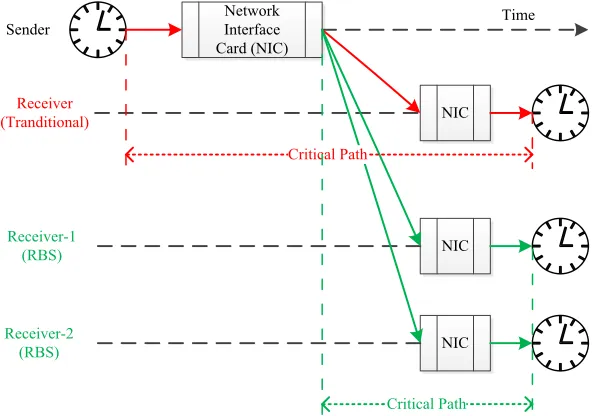
The main idea of RBS is that a designated root node would broadcast a beacon to all the other nodes. Multiple nodes would receive the beacon simultaneously and note their local time upon reception. And these receivers can also compare their clocks to one another to calculate their relative phase offsets. A most simple RBS system is usually made up of one broadcast beacon and two receivers. Two receivers will regu-larly receive timing packets issued by the broadcast beacon and will adjust their local clocks in time according to the received timing packets.
Network Interface Card (NIC)
Sender Time
NIC
NIC
NIC Receiver
(Tranditional)
Receiver-1 (RBS)
Receiver-2 (RBS)
Critical Path
Critical Path
Fig. 1. Comparison of a traditional synchronization system with RBS
sys-tem includes the sender. But in the RBS, the critical path only contains the propaga-tion and receive time uncertainty. It is because of that RBS is a receiver to receiver synchronization method, and different from the traditional sender to receiver methods. When the transmission range is not big, the propagating time is negligible. It can be considered that the reference beacon could arrive at all the receiving nodes instanta-neously. Then it can come to the conclusion that the only room for error is the receiv-er uncreceiv-ertainty.
One broadcast and two receivers forms the simplest structure of a RBS system. It can be expanded to synchronization between N receivers, where N is greater than two. In this case, more than one broadcast would be required, because of that the more the number of broadcast the higher the synchronization accuracy.
3
Design and implementation of RBS experimental system
In order to verify the validity and feasibility of the RBS protocol, an experimental system has been designed and implemented. In the experimental system, the RBS synchronization process is initiated by the broadcast beacon.The broadcast beacon will broadcast a time_sync packet at time T0 to the receivers.The time_sync packet
cacontains a pulse-per-second signal's logic level ("0" or "1") retained by the broad-cast beacon and the time T0 when it was sent. These receivers will receive and
disas-semble the time_sync packets periodically, and fine tune their local clocks acorrding to the received time_sync packet, as well as produce and maintain their own pulse-per-second signal.
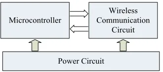
Beacause the most simple RBS system is usually made up of one broadcast beacon and two receivers, so three nodes have been developed, including one sender and two receivers. Both of the sender and receiver include a power circuit, a wireless commu-nication circuit and a microcontroller. Fig.2 gives the brief design scheme of the node in the RBS time synchronization experimental system.
Power Circuit
Microcontroller Communication Wireless Circuit
Fig. 2. Scheme of System
fixed at 3.3V, which is split subsequently into multiple parts and transported to other circuit modules (the microcontroller and the wireless communication circuit).
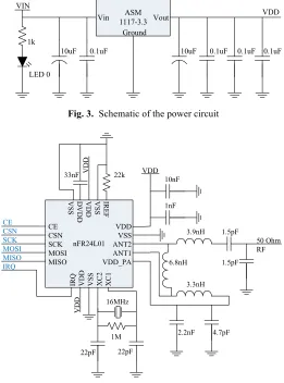
In the RBS experimental system, wireless communication circuit is designed based on a single chip 2.4GHz transceiver nRF24L01, which is produced by Nordic Semi-conductor. The transceiver consists of a fully integrated frequency synthesizer, a power amplifier, a crystal oscillator, a demodulator, a modulator and an enhanced shock burst protocol engine. Output power, frequency channels and protocol setup are easily programmable through a SPI interface. Its current consumption is very low, only 9.0mA at an output power of -6dBm and 12.3mA in the RX mode.
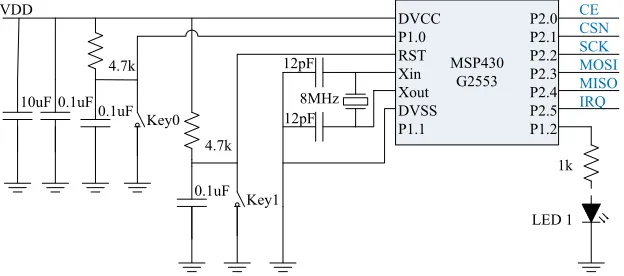
In order to program and control the nRF24L01, a Texas Instruments 16-bit micro-controller MSP430G2553 is employed in our design, as shown in Fig.5. The interface of nRF24L01 and MSP430G2553 is shown in Fig.4 and Table I.
VIN 1k LED 0 ASM 1117-3.3 Vout Vin Ground
10uF 0.1uF 10uF 0.1uF 0.1uF 0.1uF
VDD
Fig. 3. Schematic of the power circuit
nFR24L01 VDD VSS ANT2 ANT1 VDD_PA CE CSN SCK MOSI MISO IREF VSS VDD DVDD VSS
IRQ VDD VSS XC2 XC1
16MHz 1M 22pF 22pF VDD CE CSN SCK MOSI MISO IRQ 3.9nH 6.8nH 3.3nH 1.5pF 1.5pF 2.2nF 4.7pF 50 Ohm RF 1nF 10nF VDD
33nF VDD 22k
MSP430 G2553 CE CSN SCK MOSI MISO IRQ DVCC P1.0 RST Xin Xout DVSS P1.1 P2.0 P2.1 P2.2 P2.3 P2.4 P2.5 P1.2 10uF 0.1uF VDD Key0 4.7k 0.1uF Key1 4.7k 0.1uF 12pF 12pF8MHz LED 1 1k
Fig. 5. Schematic of the microcontroller circuit
Table 1. Interface of nRF24L01 and MSP430G2553
Name Pin Functon Description
CE Digital Input Chip enable
IRQ Digital Output Maskable interrupt pin
CSN Digital Input SPI chip select
SCK Digital Input SPI clock
MOSI Digital Input SPI slave data input
MISO Digital Output SPI slave data output, with tri-state option
The CE (Chip Enable) pin is used to set the nRF24L01 into TX or RX mode. The nRF24L01 also has an active low interrupt pin (IRQ). When MSP430G2553 writes '1' to the interrupt source of nRF24L01, the IRQ pin will go inactive. The interrupt mask part of the CONFIG register in nRF24L01 is used to mask out the interrupt sources that are allowed to set the IRQ pin low. By setting one of the MASK bits high, the corresponding interrupt source will be disabled.
The SPI interface of nRF24L01 is a standard SPI interface with a maximum data rate of 10Mbps.The SPI bus is usually a high-speed serial bus that connects a master device to one or more slave devices. In our design, the MSP430G2553 is the master and the nRF24L01 is the slave. All communications are initiated by the master. The SPI protocol behaves like a ring buffer, so that whenever the master sends a byte to the slave, the slave sends a byte back to the master. The slave can use this behavior to return a status byte, a response to a previous byte, or null data (the master may choose to read the returned byte, or ignore it). The bus operates on a 4-wire interface as fol-lows:
1.CSN (SPI Chip Select) selects which slave should listen on the bus. Many slaves can be connected to the bus (they share the other three wires), but only one can be selected to communicate at a time.
MSP430G2553. It determines the speed at which the SPI connection transmits da-ta.
3.MOSI (SPI Slave Data Input) carries data bits from the MSP430G2553 to the nRF24L01.
4.MISO (SPI Slave Data Output) carries data bits from the nRF24L01 to the MSP430G2553.
In our design, the wireless communication circuit can be set up as a receiver or transmitter by the MSP430G2553. When the communication circuit works in the receiver mode, the nRF24L01 is configured as a RX mode. To enter this mode, the nRF24L01 must have the PWR_UP bit set high, PRIM_RX bit set high and the CE pin set high. In this mode the receiver demodulates the signals from the RF channel, constantly presenting the demodulated data to the baseband protocol engine. The baseband protocol engine constantly searches for a valid packet. If a valid packet is found (by a matching address and a valid CRC) the payload of the packet is presented in a vacant slot in the RX FIFO. If the RX FIFO is full, the received packet is discard-ed. When the communication circuit works in the transmitter mode, the nRF24L01 is configured as a TX mode. The TX mode is an active mode where the nRF24L01 transmits a packet. To enter this mode, the nRF24L01 must have the PWR_UP bit set high, RIM_RX bit set low, a payload in the TX FIFO and, a high pulse on the CE for more than 10µs.
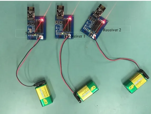
Based on the system scheme and the circuit schematics mentioned above, a small-scale RBS experimental system has been developed, which contains one sender and two receivers, just as shown in Fig.6.
Fig. 6. Photograph of the RBS experimental system
4
Experiments
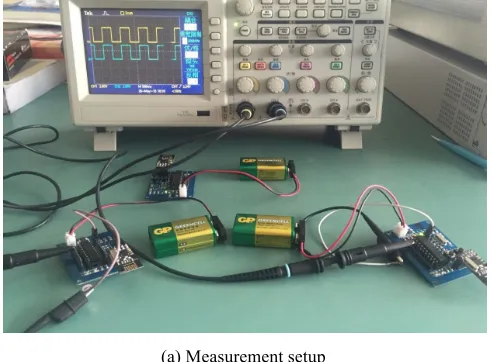
In order to make it easier to test the performance of the time synchronization exper-imental system, a synchronous effect indicator is designed in the microcontroller circuit. It contains a light emitting diode and a current limiting resistor, which are connected in series and fixed to the microcontroller's P1.2. Each receiver outputs a pulse-per-second signal with a duty ratio of 50% at the P1.2 pin based its local clock. So it is reasonable to assess the synchronization effect by measuring the two pulse-per-second signals use oscilloscope or time interval counter.
In order to gurantee the accuracy of the measurement, the measurement instru-ments usually need several hours for warm-up after turning on. In our experiment, all of the measurements were carried out four hours after the experimental system and the measurement instruments were powered on.
(a) Measurement setup
(b) Measurement result
The Fig.7 gives the measurement result of oscilloscope TDS2024B, where we can observe both the rising or falling edges of the two pulse-per-second signals are basi-cally the same. And by measuring the time interval between the rising edges of two pulse-per-second signals using a time interval counter, we can get more accurate measurements.
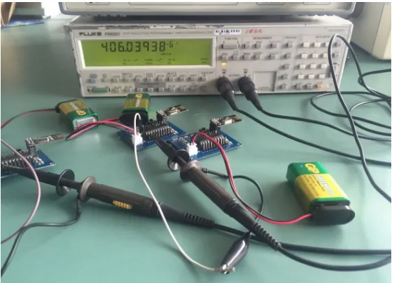
According to the real measurement result of the time interval counter FLUKE PM6681, the time synchronization error between the two receivers is about 406 mi-croseconds, just as shown in Fig.8. The error is mainly due to the individual differ-ences of the electronic components in the receiver. For example, the actual frequen-cies of the crystal oscillators in two receivers are unlikely to be exactly the same, which will cause the microcontroller's processing speed to be different. So the receiv-ers will spend different time on the same task, even if they receive the synchroniza-tion instrucsynchroniza-tions from the sender at the same time.
Fig. 8. Measurement using time interval counter PM6681
5
Conclusions
In summary, the significance of our work lies in: (1) A compact reference broad-cast time synchronization experimental system based on RBS protocol is designed and implemented. (2) A variety of experimental schemes are designed to evaluate the time synchronization accuracy of the system. (3) Combing theoretic analysis and experiment, the reasons of the RBS time synchronization error are analyzed. The experimental results show that the local clocks of those nodes with a distance less than 200 meters can be adjusted synchronously with a time synchronization error less than 410 microseconds. The circuit design scheme of the time synchronization exper-imental system proposed in this paper may be taken as technical references for the planning and designing of low cost, miniaturization and high accuracy nodes in wire-less sensor networks.
The energy limitation of nodes is one of the common features of WSN. Our main research plan in the future is to reduce the energy consumption of nodes as much as possible under the premise of ensuring the synchronization accuracy of the time syn-chronization algorithm. The energy saving schemes or protocols including the hard-ware power control, on-demand synchronization mechanism, intelligent wake-up mechanism to improve the energy efficiency in different aspects will be focused on. The verification and evaluation will be done through a series of computer simulations and practical experiments.
6
Acknowledgment
This work is partially supported by the National Natural Science Foundation of China (No.11403018) and the Open Fund of Key Laboratory of Precision Navigation and Timing Technology of National Time Service Center (No.2014PNTT04). The authors also gratefully acknowledge the helpful comments and suggestions of the reviewers, which have improved the presentation.
7
References
[1] Ali A.S., Ahmad M. (2017). Efficient, Single Hop Time Synchronization Protocol for Randomly Connected WSNs, IEEE Wireless Communications Letters, 6(2), pp. 70-173. [2] Sun Y.I., Zeng L.K., Wu X., Lu J., Sun Y.U. (2015). Timing Synchronization Algorithm
Based on Clock Skew Estimation for WSN, Journal on Communications, 36(9), pp.26-33. [3] Wang F.Q., Zeng P., Yu H.B., Xiao Y. (2013). Random Time Source Protocol in Wireless
Sensor Networks and Synchronization in Industrial Environments, Wireless Communica-tions and Mobile Computing, 13(8), pp.798-808. https://doi.org/10.1002/wcm.1144 [4] Swain A.R., Hansdah R.C. (2015). A Model for the Classification and Survey of Clock
Synchronization Protocols in WSN, Ad Hoc Networks, 27, pp.219-241. https://doi.org/10.1016/j.adhoc.2014.11.021
Health Monitoring, Journal of Network and Computer Applications, 83, pp.181-189. https://doi.org/10.1016/j.jnca.2017.01.004
[6] Beniwal M., Singh R.P., Sangwan A. (2016). A Localization Scheme for Underwater Sen-sor Networks Without Time Synchronization, Wireless Personal Communications, 88(3), pp.537-552. https://doi.org/10.1007/s11277-016-3175-2
[7] Elson J., Romer K. (2003). Wireless Sensor Networks: A New Regime for Time Synchro-nization, Computer Communication Review, 33(1), pp.149-154. https://doi.org/10.1145/ 774763.774787
[8] Xu C.N., Zhao L., Xu Y.J., Li X.W. (2007). Time Synchronization Improvement Strategy for Wireless Sensor Networks, Chinese Journal of Computers, 30(4), pp.514-523. [9] Xiao L., Cheng L.J., Wang F.B. (2008). Low Cost Time Synchronization Algorithm for
Wireless Sensor Networks, Computer Research and Development, 45(1), pp.126-130. [10] Chaudhari Q.M., Serpedin E., Qaraqe K. (2008). On Maximum Likelihood Estimation of
Clock Offset and Skew in Networks with Exponential Delays, IEEE Transactions on Sig-nal Processing, 56(4), pp.1685-1697. https://doi.org/10.1109/TSP.2007.910536
[11] Shi X., Zhao X.M., Hui F., Yang L. (2012). A WSN Time Synchronization Algorithm Ori-ented Clustering Real-time Monitoring Application, Journal of Sichuan University (Engi-neering Science Edition), 44(25), pp.121-129.
[12] Gopi K.Y., Awadhesh K., Akash R. (2015). Analysis of Time Synchronization Protocols for Wireless Sensor Networks: A Survey, International Journal of Computer Science and Mobile Computing, 4(5), pp.1062-1068.
[13] Kosanovic M.R., Stojcev M.K. (2012). RPATS-Reliable Power Aware Time Synchroniza-tion Protocol, Microelectronics Reliability, 54(1), pp.1303-1315.
[14] Djenouri D., Bagaa M. (2016). Synchronization Protocols and Implementation Issues in Wireless Sensor Networks: A Review, IEEE Systems Journal, 10(2), pp.617-627. https://doi.org/10.1109/JSYST.2014.2360460
8
Authors
Sheng Tang, Zunzun Li, and Pengfei Dong are with School of Information Sci-ence and Technology, Northwest University, Xi’an, China.
Jing Ke is with National Time Service Center, Chinese Academy of Sciences, Xi’an, China([email protected]).