Http://www.ijetmr.com©International Journal of Engineering Technologies and Management Research [123]
POWER REDUCTION TECHNIQUES IN VLSI
Mehar Sharma 1, Neeraj Gupta 2, Rashmi Gupta 2
1
M.Tech Student, Amity School of Engineering & Technology, India
2
Assistant Professor, Amity School of Engineering & Technology Amity University Haryana, Gurugram, India
Abstract:
The paper investigates different level of techniques used for power reduction in VLSI. Before, most of the researches were oriented towards bringing about high speed and miniaturization. At present, because of the increasing trend of compact devices, the requirement for low power consuming circuits have also increased. This necessitates the need to align the research for reducing power dissipation in VLSI circuits. In the given paper we will briefly discuss about the different types of power reduction techniques at design abstraction level which are adopted in industries now-a-days. The comparison of traditional techniques and present techniques
are also covered in this paper.
Keywords: Gating Technique; Back Biasing; FET; Multi-Threshold Devices; Power Dissipation.
Cite This Article: MEHAR SHARMA, NEERAJ GUPTA, and RASHMI GUPTA. (2018). “POWER REDUCTION TECHNIQUES IN VLSI.” International Journal of Engineering Technologies and Management Research, 5(2:SE), 123-129. 10.29121/ijetmr.v5.i2.2018.633.
1. Introduction
With the demand of addition of more and more system on chip, the number of transistors are getting added which leads to the increase in power dissipation in the devices [1]. Two main features of low power design is battery lifeline; specially in portable devices and the other one is reliability .Power consumption in VLSI devices are of four types which are given by
1) Dynamic power consumption 2) Static power consumption 3) Leakage power consumption 4) Static power consumption
Http://www.ijetmr.com©International Journal of Engineering Technologies and Management Research [124] 2. Low Power Design
Power loss is the main constrain when it comes to portability. Exigency for more features and extended battery life has been increased. Around 2/3 populations demands for longer stand by time as primary mobile phone feature [1][2]. Power matters in SOC because of the following concerns
1) Environmental concerns. 2) Battery life
3) Digital noise immunity 4) Packaging cost
5) Cooling cost
Principles of low power designs are given as
1) Using higher frequency device and using them in lowest possible frequency 2) Disconnecting the power supply when system is not in use
3) Controlling power dissipation at architectural level
4) Using pipelining and parallelism to lowest required frequency of operation Using lowest possible supply voltage
Table 1: Power Reduction Techniques
Traditional Techniques
Dynamic Power Reduction
Leakage Power Reduction Other Power
Reduction Technique
Clock gating Clock gating Minimize usage of VT cells Minimize oxide devices Variable frequency Variable frequency Back biasing Power efficient circuit Variable voltage
supply
Variable voltage supply
Reduce oxide thickness
Variable device threshold
Variable island Use FET
3. Traditional Low Power Techniques
To reduce the power usage, clock frequency, reduction of switching activity, voltage scaling is very widely used.
3.1.Clock Gating
This technique is a very popular technique mainly used for the reduction of dynamic power dissipation [2]. In clock gating technique, more logic gates are added to the circuits to trim the clock tree. By paring the clock, the clock defuses some parts of the circuits so that there is no switching in the flip flops.
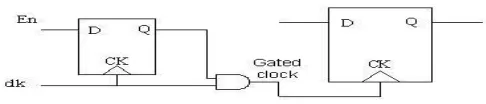
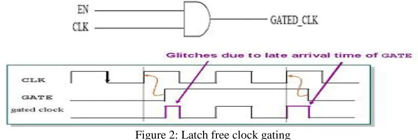
Http://www.ijetmr.com©International Journal of Engineering Technologies and Management Research [125] Latch based clock gating append a level sensitive latch which is designed in a way to hold the enabled signal from the active edge of the clock unless the generation of complete clock pulse.
Figure 2: Latch free clock gating
AND and OR gate is used for designing latch free clock gating. If the enabled signal goes inactive between the clock pulses then gate clock either generate multiple clock pulses or can terminate prematurely.
3.2.Variable Frequency
Variable frequency drive (VFD) is also called as adjustable frequency devices. it is used in electro mechanical drive systems so to control the speed of AC motors and torque. It is been done by varying inputs given to the motors. These inputs can be frequency or voltage. VFD is use almost in every small appliance to compressors as about quarter of the electrical energy is used in industries by the motors.
By the mean of VFD, many motors application that are supplied from AC line power can save power when work at different variable.
VFD consist of following three components AC Motor
Controller
Operator interface
Main two benefits of VFD are energy saving and control performance.
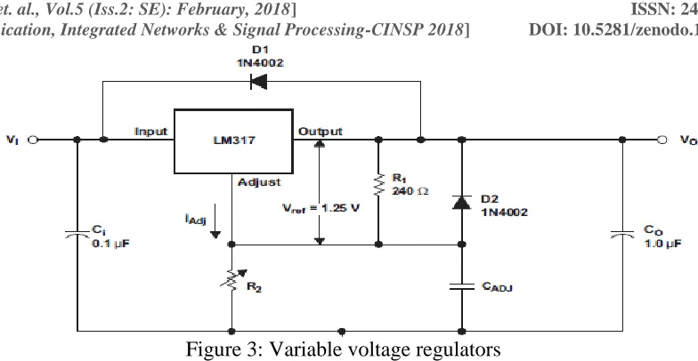
3.3.Variable Voltage Supply
Http://www.ijetmr.com©International Journal of Engineering Technologies and Management Research [126] Figure 3: Variable voltage regulators
3.4.Variable Device Threshold
This technology controls the threshold voltage by substrate bias control. The investigation of the characteristics of variable threshold voltage is been done by device simulation. Thus if the threshold voltage is decreased, the drive current is increased and decrease the degradation due to the series connected configuration.
Figure 4: Variable Threshold
By adjusting the body biased voltage, as shown in fig 4, threshold voltage of both the devices can be increased, thus reducing the sub threshold voltage in standby mode.
4. Dynamic Power Reduction
Power utilization in CMOS is generally of three types, static power consumption, dynamic power consumption and leakage current .Dynamic power equation is given by:
P=ACV2F
Http://www.ijetmr.com©International Journal of Engineering Technologies and Management Research [127] 4.1.Clock Gating
It is mostly used in sequential circuits for reduction of dynamic power. The main principle of clock gating is that it reduces the consumption of clock signals that is switching power of flip flops [2]. By introducing clock gating, the unnecessary clock switching of the adders can be removed or avoided during clock cycles. Up to the half that is 50% or sometimes even more of dynamic power can be wasted during the clock buffering [2][3]. This is because of the higher toggle rate in the system, the cock buffers usage is more in a system and clock buffers minimize clock delay.
4.2.Power Efficient Technique
Power efficiency can be achieved by the reduction of power loss. Reducing power loss will result in the financial cost saving to consumers if the power savings offset any additional costs of implementing and power efficient technology. Power efficiency and power renewal are two pillars of sustainable power. Power can be analyze at circuit and gate level. There are certain techniques for low power
4.2.1. Adiabatic Circuits
The principle of adiabatic circuits is that they reuse the power instead of dissipating. This is done by restraining the shape and length of the signal transition energy. Because of the thermodynamically invisible nature, diodes are not used in the designing of the adiabatic circuits.
4.2.2. Logic Design of Low Power
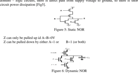
In static CMOS circuit, the power dissipation is about 10% of the total power consumption. in dynamic circuits, as there is no direct dc supply to ground, we don’t face such problem but in domino – logic circuits, there is direct path from supply voltage to ground, so there is short circuit power dissipation [Fig5].
Figure 5: Static NOR
Z can only be pulled up id A=B=0V
Z can be pulled down by either A=1 or B=1 (or both)
Http://www.ijetmr.com©International Journal of Engineering Technologies and Management Research [128] 5. Leakage Power Reduction
In on-chip devices, leakage power reduction has become very challenging. Decrease of the threshold voltage current has resulted in the increase of the subthreshold leakage current thus increase the leakage power dissipation [3]. Subthreshold leakage current is given as the drain to source current of a transistor operating in the weak inversion region. Dependence of device parameters on subthreshold leakage current is given in following table.
Table 2: Subthreshold Leakage Current
PARAMETERS DEPENDENCE
Temperature (T) Exponential increase
Transistor length (L) Inversely proportional Transistor width (W) Directly proportional Input voltage (Vgs) Exponential increase
Transistor threshold voltage (Vth) Increase by the order of magnitude with 100mv decrease
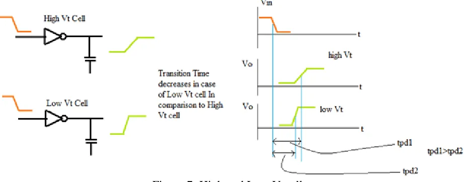
5.1.Use of Low Vt Cell and High Vt Cell
For reducing power while maintain speed, multiple Vt devices are used. low Vt devices are used for designing high circuit path , on other hand high Vt is applied to gates in order to reduce leakage current .Multiple threshold technique is mostly been taken into consideration because it does not require any change in SOC architecture ,it instead depends on how the designer judiciously use low Vt cell[4]. The advantage of low Vt cell is that it has low timing but higher leakage current and high Vt cells have low leakage current but high timing as shown in fig7. So as high Vt cells have more timing so they are used where timing is relaxed where as low Vt cells are used at time-critical places [5].
Figure 7: High and Low Vt cell
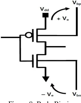
5.2.Back Biasing
Http://www.ijetmr.com©International Journal of Engineering Technologies and Management Research [129] in tube state. Back biasing is also known as substrate biasing [6]. . With the improvement in the techniques, the substrate is biased to increase transistor threshold. Thus thereby minimizing leakage. In PMOS, the body of transistor is biased to a voltage higher than Vdd. In NMOS, the body of transistor is biased to a voltage lower than Vss.
Figure 8: Body Biasing
6. Conclusion
Power reduction at various levels of abstraction, namely the circuit, logic, architecture and system level is been estimated .power consumption diffusion among clock distribution, memories, gates, interconnections are analyzed. Lowering power dissipation at every abstraction level is at focal point of industrial research.
References
[1] B. Pouya, A. Crouch, "Optimization Trade-offs for Vector Volume and Test Power", Proc. Int'l Test Conf., pp. 873-881, 2000.
[2] L. Benini, M. Favalli, G. De Micheli, "Design for testability of gated-clock FSM's", Proc. European Design and Test Conf., Mar. 1996.
[3] Pedram Massoud, Abdollahi Afshin, "Low Power RT-Level Synthesis Techniques: A Tutorial" in, Dept. of Electrical Engineering, University of Southern California.
[4] A. Chandrakasan, "Design considerations and tools for low-voltage digital system design", Proc. 33rd. Design Automation Conference, pp. 113-118, 1996.
[5] M. Horiguchi, "Switched-source-impedance CMOS circuit for low standby subthreshold current giga-scale LSI's", IEEE J. Solid-State Circuits, vol. 28, pp. 1131-1135, Nov. 1993.
[6] Effect of Shock Polarity on Ventricular Defibrillation Threshold Using a Transvenous Lead System, Strickberger et al, JACC, vol. 24, No. 4, Oct. 1994, pp. 1069 1072.
*Corresponding author.