International Doctorate School in Information and Communication Technologies
DISI - University of Trento
Novel Design Solutions for
High Reliability
RF MEMS Switches
Francesco Solazzi
Advisor:
Dr. Benno Margesin
Head of MEMS Group - FBK
Co-Advisor:
Dr. Alessandro Faes
This doctorate thesis focuses on the analysis, design and characteriza-tion of Radio-Frequency (RF) Micro-Electro-Mechanical System (MEMS) switches for space applications. The work was inspired and supported by the European Space Agency (ESA) Contract No. ITT AO/1-5288/06/NL/GLC High Reliability Redundancy Switch. The main purpose of the project is the design and realization of high-reliability RF MEMS switches for satel-lite payload redundancy networks. Up to now, the common satelsatel-lite archi-tecture implements redundancy networks by means of bulky devices. RF MEMS switches allow for extremely miniaturized networks along with out-standing performances in terms of losses, power consumption and linearity, not really achievable with solid state devices. As requirements for such an application, RF MEMS switches have to survive under extremely harsh environmental and operating conditions. In particular the device should handle continuous bias voltage (at least for 10 years), 5 W of RF input power and around 1000 actuation cycles without meaningful electrical and mechanical failure. The thesis proposes novel mechanical solutions to ac-complish this task, exploiting active restoring mechanisms able to restore the previous status of switch in case of reversible failure. This work also provides a deep insight on the main reliability aspects of a RF MEMS device such as dielectric charging, contact degradation and power handling.
Keywords
[RF MEMS Switches, Redundancy Networks, Active restoring mechanisms,
Conference Papers
• P. Farinelli, F. Solazzi; C. Calaza, B. Margesin, R. Sorrentino, “A Wide Tuning Range MEMS Varactor Based on a Toggle Push-Pull
Mechanism”, Proceedings on 38th European Microwave Conference (EuMC), 2008, pp. 474-477, Amsterdam, 27-28 Oct. 2008.
• F. Solazzi, P. Farinelli, B. Margesin, R. Sorrentino, “35 GHz Analog Phase shifter based on push-pull Toggle MEMS Varactor”, Proceedings on 9th International Symposium on RF MEMS and RF Microsystems, Heraklion, 2008.
• F. Solazzi, A. Repchankova, P. Farinelli, J. Iannacci, A. Faes, B. Margesin, “Contact Modeling of RF MEMS Switches based on FEM
Simulations”, Proceedings on 10th International Symposium on RF MEMS and RF Microsystems, Trento, 2009.
• A. Tazzoli, E. Autizi, M. Barbato, F. Solazzi, J. Iannacci, P. Farinelli, F. Giacomozzi, B. Margesin, R. Sorrentino, G. Meneghesso, “Impact
of Continuous Actuation on the Reliability of Dielectric-less Ohmic
RF MEMS Switches, Proceedings on 10th International Symposium on RF MEMS and RF Microsystems, Trento, 2009.
• A. Tazzoli, E. Autizi, M. Barbato, G. Meneghesso, F. Solazzi, P. Farinelli, F. Giacomozzi; J. Iannacci, B. Margesin, R. Sorrentino,
switches during continuous actuation stress”, Proceedings of the Euro-pean Solid State Device Research Conference, (ESSDERC) 2009, pp. 343-346, 14-18 Sept. 2009.
• J. Iannacci, D. Macii, B. Margesin, A. Repchankova, F. Solazzi, ”Una procedura per la stima degli effetti dell’incertezza di processo
sulle prestazioni di dispositivi RF-MEMS”, Atti del XXVI Congresso Nazionale del Gruppo Misure Elettriche ed Elettroniche, pp. 121-122, Salerno,16-19 Sept. 2009.
• C. Palego, F. Solazzi, S. Halder, J.C.M. Hwang, P. Farinelli, R. Sorrentino, A. Faes, V. Mulloni, B. Margesin, “Analysis of Power
Ca-pacity of RF MEMS Capacitive Shunt Switches Fabricated on Silicon
or Quartz Substrates”, Proceedings on 11th International Symposium on RF MEMS and RF Microsystems, Otranto, 2010.
• F. Solazzi, C. Palego, S. Halder, J.C.M. Hwang, A. Faes, V. Mulloni, B. Margesin, P. Farinelli, R. Sorrentino, “Electro-thermal analysis of
RF MEM capacitive switches for high-power applications,” Proceed-ings of the European Solid-State Device Research Conference (ESS-DERC), 2010, pp. 468-471, 14-16 Sept. 2010.
• C. Palego, F. Solazzi, S. Halder, J.C.M. Hwang, P. Farinelli, R. Sorrentino, A. Faes, V. Mulloni, B. Margesin, “Effect of substrate
on temperature range and power capacity of RF MEMS capacitive
switches,”Proceedings on European Microwave Conference (EuMC), 2010, pp. 505-508, 28-30 Sept. 2010.
• F. Solazzi, A. Tazzoli, P. Farinelli, A. Faes, V. Mulloni, G. Meneghesso, B. Margesin, “Active recovering mechanism for high performance RF
Tazzoli, G. Meneghesso, “Modeling and characterization of a
circular-shaped energy scavenger in MEMS surface micromachining
technol-ogy,”Proceedings on SPIE Microtechnology 2011, Prague, April 2011.
• F. Solazzi, G. Resta, V. Mulloni, B. Margesin, P. Farinelli, “In-fluence of beam geometry on the dielectric charging of RF MEMS
switches,”Accepted at European Microwave Conference (EuMC), 2011, pp.93-96, 28-30 Oct. 2011.
Journal Papers
• F. Solazzi, C. Palego, S. Halder, J.C.M. Hwang, A. Faes, V. Mulloni, B. Margesin, P. Farinelli, R. Sorrentino, “Effect of the Substrate on
RF Power-Handling Capability of Micro-Electromechanical
Capaci-tive Switches”, Accepted for publication on Solid State Electronics Journal - Special Issue from ESSDERC/ESSCIRC Conference 2010, Elsevier.
• F. Solazzi, A. Tazzoli, P. Farinelli, A. Faes, V, Mulloni, G. Meneghesso, B. Margesin, “Design and characterization of an active recovering
mechanism for high performance RF MEMS redundancy switches”,
During my Ph.D activity I met an amazing number of people who really
gave a fundamental contribution to my personal and professional growth.
I do not know if I will be able to really thank all of them.
First of all, a special and deep acknowledgment is for my advisor Benno
Margesin. He was really a mentor in the world of Research. His guidance
and his constant encouragement were always precious, and his extensive
scientific knowledge of almost everything never stops surprising me.
I do not know how I have to do to pay back my colleague and co-advisor
Alessandro Faes for the constance and patience he showed me in reviewing
this thesis and almost all the papers I published.
Then I absolutely have to thank all the MEMS group. First, Jacopo
Iannacci, whose professional guidance and also friendship helped me a lot
in overcoming some critical moments. A special thank goes to Flavio
Gi-acomozzi, who welcomed me for first in FBK when I was just a master
student. His valued suggestions and huge experience are still fundamental
to make all my designs work.
I am deeply in debt with my colleagues Viviana Mulloni and Sabrina
Colpo. I was often stressful towards them, but both have always been
helpful and I always received a positive answer for anything I asked. I am
in debt too with Giuseppe Resta, whose contribution in the measurement
setups was fundamental for my recent scientific works.
I want also to thank my past colleagues, Carlos Cabana (who
intro-duced me in the finite element method world for first), Parisa Savadkoohi
and Alena Repchankova (who are now pursuing their carriers outside the
Giordano, and Abdul Qureshi.
I am grateful to Prof. Roberto Sorrentino from University of Perugia for
his support and the opportunity he gave me when he proposed me to pursue
a Ph.D in Trento, and especially when he provided me the connection for
my US experience. A big thank goes to Paola Farinelli from RF Microtech,
who introduced me in the MEMS World for first. She was the first person
who found a researcher in me. Her constant support during all my activity
and her expertise helped me really a lot in acquiring a wide and complete
vision of all my research field. I reserve a special thanks to Augusto Tazzoli
from University of Padova, who really supported me with suggestions and
hard work at any hours of the day in most of my published papers.
I would like also to thank all the people I met during my precious
experience in United States. I am grateful to Prof. James Hwang who
accepted me as a member of his research group, making me feel like part of
it from the very beginning. I want to express all my deep acknowledgment
to Cristiano Palego, David Molinero Giles and Bora Baloglu, who behaved
with me like a family during my stay in Bethlehem. I will never forget
their outstanding contribution to my professional growth. A big thanks
also to the other members of the CSTL group at Lehigh University, Steven
Peng, Weike Wang, Guanghai Ding, Xi Luo, Subrata Halder, Cheng Chen
and Renfeng Jin.
I want also to acknowledge all the people from DISI department who
contributed to my professional grow. In particular, a special thanks is for
Prof. Gianfranco Dalla Betta, Prof. Dario Petri and Dr. David Macii.
A final thank goes to all the people from MTLab and FBK and to all
that I can dodge bullets?” Morpheus: ”No Neo. I’m trying to tell you
that when you’re ready, you won’t have to.”
List of publications 5
1 Introduction 1
1.1 Radio Frequency MEMS . . . 2
1.2 Reliability of RF MEMS . . . 3
1.3 Analysis and solutions . . . 5
1.4 Structure of the Thesis . . . 6
2 State of the art 7 2.1 Introduction . . . 7
2.2 RF MEMS switches . . . 8
2.2.1 Basics of RF MEMS . . . 8
2.2.2 Advantages of RF MEMS . . . 11
2.2.3 RF MEMS today in research and market . . . 13
2.2.4 RF MEMS applications . . . 16
2.3 Redundancy networks for space applications . . . 18
2.4 Reliability of RF MEMS . . . 21
2.4.1 Definition . . . 21
2.4.2 Electrical-induced failures . . . 23
2.4.3 Operational-induced failures . . . 25
2.4.4 Mechanical failure modes . . . 26
2.4.6 RF MEMS Packaging . . . 29
2.5 Review of the main anti-stiction mechanisms . . . 30
2.6 Advances in FBK manufacturing process . . . 35
2.7 Conclusion . . . 39
3 Modeling of RF MEMS switches 41 3.1 Introduction . . . 41
3.2 Mechanical model . . . 41
3.2.1 Linear stiffness . . . 41
3.2.2 Effect of residual stress . . . 45
3.2.3 Electrostatic model . . . 48
3.3 Electromagnetic model . . . 51
3.4 Simulation tools . . . 57
3.4.1 Circuit simulators . . . 57
3.4.2 Finite element method . . . 58
3.4.3 Method of Moments . . . 60
3.5 Case studies . . . 61
3.5.1 Benchmark devices . . . 61
3.5.2 Electromechanical model of a capacitive switch . . 62
3.5.3 Residual stress modeling . . . 65
3.5.4 Contact modeling for ohmic switches . . . 68
3.5.5 2.5D electromagnetic model of a ohmic switch . . . 70
3.5.6 3D electromagnetic model of a capacitive switch . . 72
3.6 Conclusions . . . 74
4 Long-Term Stress Reliability 75 4.1 Introduction . . . 75
4.2 Review of contact degradation mechanisms . . . 76
4.3 Review of dielectric charging models . . . 79
4.4.2 Experimental . . . 93
4.4.3 Discussion . . . 97
4.5 Conclusions . . . 101
5 Power Handling 103 5.1 Introduction . . . 103
5.2 Basic Theory . . . 104
5.3 State-of-the-art for high power switches . . . 107
5.4 Multiphysics Analysis of a FBK capacitive switch . . . 110
5.4.1 The Multiphysics approach . . . 110
5.4.2 Device under test . . . 111
5.4.3 Simulation Procedure . . . 113
5.4.4 Results . . . 116
5.5 Experimental validation . . . 118
5.6 Self-biasing . . . 122
5.7 Self-heating . . . 125
5.8 Pull-in shift estimation . . . 128
5.9 Conclusions . . . 131
6 Design Solutions for Redundancy Switches 133 6.1 Introduction . . . 133
6.2 Toggle mechanism concept . . . 134
6.2.1 Description . . . 134
6.2.2 Model . . . 135
6.2.3 Optimization . . . 142
6.3 Experimental results on toggle switch . . . 146
6.3.1 Fabrication . . . 146
6.3.2 Characterization . . . 148
6.4 Ohmic toggle switch . . . 157
6.5 Toggle mechanism for bi-stable switches . . . 159
6.5.1 Buckling of a compressive beam . . . 160
6.5.2 The Guckel Ring . . . 161
6.5.3 Bistability criteria . . . 164
6.5.4 Switch design and characterization . . . 167
6.5.5 Result discussion . . . 172
6.6 Conclusions . . . 175
7 Conclusion 177
2.1 List of state-of-the-art RF MEMS switches. . . 14
3.1 Finite element properties used in ANSYS simulations. . . . 63
3.2 ANSYS finite element properties used to simulate stress and
stress gradient in the cantilever beams manufactured in FBK. 67
3.3 ANSYS finite element properties used to simulate the
con-tact in the ohmic switches manufactured in FBK. . . 68
3.4 Material properties and settings used in Momentum and
HFSS for the simulations of FBK switches. . . 72
4.1 Equivalent circuit parameters of the dielectric-less switches
under test. . . 85
4.2 Finite elements properties used in the FEM simulation of
the stoppers effect . . . 89
4.3 List of parameters extracted from the Eq. (4.16) fitting with
average measured pull-out variations. . . 98
5.1 Substrate properties and equivalent circuit parameters. . . 113
5.2 Air bridge dimensions and electromechanical properties. . . 114
5.3 Lumped Thermal Parameters extracted from simulation
re-sults. . . 127
6.1 Geometrical dimensions and material properties of the
6.2 Mechanical Properties of the capacitive toggle switch. . . . 148
6.3 Electromagnetic properties and equivalent circuit
parame-ters of the capacitive toggle switch. . . 150
6.4 Voltage shift fitting parameters. . . 156
6.5 Geometrical dimensions of the ohmic toggle switch. . . 158
6.6 Geometrical dimensions of the bistable toggle device. . . . 169
6.7 Finite elements properties used in the ANSYS simulations
2.1 RF switches in shunt configuration: a) OFF state and b)
ON state. . . 10
2.2 RF switches in series configuration: a) OFF state and b)
ON state. . . 10
2.3 Pictures of state-of-the-art RF MEMS devices. . . 15
2.4 Pictures of state-of-the-art RF MEMS circuits. . . 16
2.5 Tunable 4-bit filter based on RF MEMS switched capacitors. 17
2.6 Examples of RF MEMS matrices. . . 18
2.7 (a) Single Pole Double Throw(SPDT), and (b) Single Pole
n Throw switch unit schemes. . . 19 2.8 (a) Typical coaxial redundancy switch matrix and switch
basic building blocks, and (b) their application in a
redun-dancy system. . . 20
2.9 Single Pole Double Throw(SPDT) switch manufactured at
FBK. . . 21
2.10 SEM photograph and schematic cross-sectional view of the
switch fabricated with top electrode. . . 31
2.11 SEM photograph and schematic of the actively-controlled
MEMS switch by DelftMEMS. . . 32
2.12 Layout and SEM images of the latching RF MEMS switch. 33
2.13 Out-of-plane bi-stable RF MEMS switch with thermal
2.14 Bi-stable metal-contact RF MEMS switch integrated in a
3-D micro-machined coplanar waveguide. . . 34
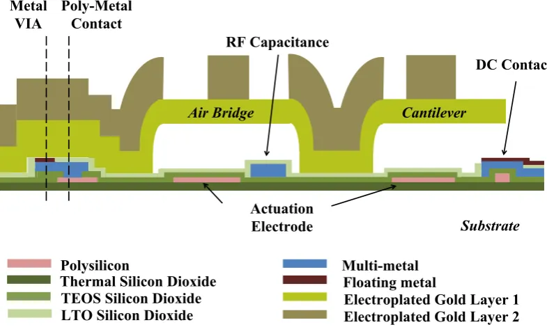
2.15 Side-view diagram of the 8-mask FBK base-line process.
The thickness dimensions are exaggerated to better
high-light the mask layers. . . 37
2.16 RF MEMS 4-inches FBK wafer on quartz substrate. . . 40
3.1 Sketch of fixed-fixed membrane used as shunt switch: (a) dimensions and reference system identification, (b) uniform
distributed load, (c) center-distributed load, and (d)
lateral-distributed load examples. . . 42
3.2 Sketch of a cantilever beam used asseries switch: (a) uniform-distributed load, and (b) tip-uniform-distributed load. . . 44
3.3 Optical profiler measurement of an array of cantilever beams
used as test structures for the monitoring of stress gradient. 47
3.4 Spring-capacitance system modeling the electro-mechanical
coupling in a MEMS switch. . . 49
3.5 Displacement along z-axis of a clamped-clamped bridge as a function of bias voltage. Note the hysteresis loop that
characterizes any kind of RF MEMS switch. . . 51
3.6 Spring-capacitance system configurations as a function of
bias voltage: (a) bridge before the actuation, (b) bridge after
the actuation, (c) bridge before the pull-out, and (d) bridge
after the pull-out. . . 52
3.7 RF switches in shunt configuration: a) ideal network and b) real network where the switch is modeled as a complex
b) real network where the switch is modeled as a complex
impedance. . . 54
3.9 Equivalent circuit of a MEMS switch in shunt configuration. 55 3.10 Equivalent circuit of a MEMS switch in series configuration. 55 3.11 Structural 20-nodes SOLID186 element definition from
AN-SYS Help. . . 59
3.12 Coupled electro-mechanical TRANS126 element definition
from ANSYS Help. . . 60
3.13 Equivalent network representation of the discretized MoM
problem . . . 61
3.14 Photo of MEMS devices used as benchmark: (a) shunt
ca-pacitive switch (”D” type), and (b) series ohmic switch (”C”
type). . . 62
3.15 Displacement solution along thez-axis of the capacitive switch shown in Fig. 3.14-a at Vbias = 0 V and 50 V. . . 64 3.16 Capacitance versus bias voltage characteristic: comparison
between measurements (symbols) and simulation (dashed
line) of the capacitive switch of Fig. 3.14-a. . . 64
3.17 Simulated pull-in (continuous line) and pull-out (dashed line)
voltage variation with residual bi-axial stress of the
capaci-tive switch from Fig. 3.14-a. . . 66
3.18 Test structure cantilever beams array: (a) finite element
model based on layered brick elements, and (b) displacement
nodal solution. . . 67
3.19 FEM simulation of the cantilever switch from Fig. 3.14-b:
(a) nodal displacement only due to stress gradient, and (b)
3.20 Contact pressure applied on contact bumps by the actuated
membrane from Fig. 3.19(b). . . 70
3.21 Comparison between S-parameters Momentum simulations
(− − −) and measurements (—) of a series ohmic switch in
OFF (a) and ON (b) state. . . 71
3.22 Comparison between S-parameters HFSS simulations (− − −) and measurements (—) of a shunt capacitive switch in
OFF (a) and ON (b) state. . . 73
4.1 Cross-section schematic of the micro-asperities of two
con-tacting surfaces. . . 76
4.2 Measurement procedure and resulting contact resistance
ver-sus contact force plot. Three contact behavioral regions are
distinguished. . . 77
4.3 (a) Plot of contact resistance versus contact force, and (b)
contact resistance evolution with respect to cycling load at
100 mA for different kind of contact materials and material
alloys. . . 79
4.4 Charge injection in to the insulating layer on a
parallel-plates capacitor MEMS model: (a) initial dipole
polariza-tion; (b) charge injection after the membrane pull-in; (c)
surface charging influence on the electrostatic force. . . 81
4.5 Pictures and corresponding equivalent circuits for (a)
air-bridge and (b) cantilever switches. The lengths of the
sus-pended beams and bias electrodes are also highlighted. . . 85
4.6 Modified Paschen’s curve: breakdown voltage on the air at
1 atm . . . 86
4.7 Cross section (a) and top view (b) geometry of the stopping
electrode of a cantilever MEMS switch. . . 88
4.9 FEM simulation of the FBK capacitive switch with
square-patterned pillars: (a) contact gap distance plot over the
actuation electrode, and (b) membrane displacement at 50 V
(dashed line) and 100 V (continuous line). The areas in gray
are out-of-scale, meaning that the minimum distance is less
than 0.32 µm. . . 91
4.10 FEM simulation of the FBK capacitive switch with X-patterned
pillars: (a) contact gap distance plot over the actuation
elec-trode, and (b) membrane displacement at 50 V (dashed line)
and 100 V (continuous line). The areas in gray are
out-of-scale, meaning that the minimum distance is less than 0.32µm. 92
4.11 Measurement setup used for the long-term stress
character-ization. . . 93
4.12 Capacitance-voltage characteristic of an air-bridge switch at
a stress time of t = 0 s (black curve) and t = ts = 8 hours
(blue curve). . . 94
4.13 Measured evolution of voltage shift (a) and narrowing (b) for
air bridge switch (in black) and cantilever switch (in red) for
pull in (continuous line) and pull-out (dashed line). Applied
voltage stress: 50 V. . . 96
4.14 Average of the pull-out voltage variation data normalized to
the corresponding stress voltages plotted versus the stress
time. . . 97
4.15 Cross-sectional view of the simulated electrostatic field
dis-tribution around the electrode of the cantilever switch when
4.16 Displacement profile of cantilever switch (a) and air-bridge
switch (b) at Vbias = 0V (dashed curve) and Vbias = 50 V
(continuous curve). . . 100
5.1 Circular-shape RF MEMS switched capacitor: (a)
micro-graph and (b) evolution of pull-in and pull-out voltages
ver-sus input RF power. . . 108
5.2 Sketch and pictures of the dielectric-block MEMS switch. . 109
5.3 High-power MEMS varactor. . . 109
5.4 High power Radant switch. . . 110
5.5 (a) Top view, and (b) cross-sectional schematic of an
elec-trostatic RF MEMS capacitive shunt switch under test. See
Fig. 2.15 for the meaning of the layer colors . . . 112
5.6 Equivalent circuit model of the capacitive RF MEMS switches
under test. . . 113
5.7 Simulation procedure for the evaluation of pull-in voltage
RF power dependence. . . 115
5.8 HFSS-simulated (dashed) vs. measured (continuous)
small-signal insertion and return losses. . . 116
5.9 Circuit (curve) and HFSS (symbols) simulated equivalent
RF voltage under the membrane in up position. . . 116
5.10 Simulated surface (a, b) current and (c, d) temperature
dis-tributions for the switches on (a, c) silicon and (b, d) quartz
under 1 W input signal at 15 GHz. . . 117
5.11 Simulated anchor-to-anchor temperature profiles along the
membrane under different RF power at 15 GHz . . . 119
5.12 Simulated temperature rise at the (left axis) center and
(right axis) anchor of the membrane on (− − −) silicon
function of different RF powers at 15 GHz. . . 121
5.14 FEM (curve) and measured (symbols) pull-in voltages VS.
RF powers slopes as a function of different frequencies. . . 121
5.15 ON state and OFF state capacitances extracted from power
measurements for (− − −) silicon and (—) quartz substrate. 122
5.16 Circuit model for both unmatched load and generator. . . 123
5.17 Equivalent thermal lumped model accounting for substrate
thermal resistance. . . 125
6.1 Sketch illustrating the cross section (a) and the top view (b)
of the device along with the corresponding description of the
layers. . . 135
6.2 Sketch illustrating the cross section of the device when (a)
zero bias voltage is applied, (b) pull in actuation or (c)
pull-out actuation occurs. . . 136
6.3 Schematic diagram representing the left half of the switch,
including forces and moments acting on the mobile electrode
in case of PI bias (a) and PO bias (b). . . 137
6.4 Schematic diagram representing the left half of the switch,
where the effect of the equivalent force due to the charging
at the PI is considered in absence of stiction (a) and in case
of stiction (b). . . 140
6.5 Toggle switch actuation voltage due to the torsion
(continu-ous line) and the bending (dashed line) of the anchor springs
as a function of spring width/length ratio for different
val-ues of spring thickness.The dashed red line marks the upper
6.6 Toggle switch actuation voltage as a function of the
mo-bile electrode length for different values of connecting lever
length. The dashed red line marks the upper limit for the
acceptable actuation voltage. . . 144
6.7 FEM displacement solution of the toggle switch for (a) PI
and (b) PO actuation when Vbias = 80 V is applied
alterna-tively to PI and PO electrodes. . . 146
6.8 Micrograph of the manufactured toggle switch with an
indi-cation of the most relevant geometrical parameters. . . 147
6.9 Profile measurement of a realized device obtained with a
Zygo Optical Profiler. (a) 3-D view. (b) Longitudinal profile
along the switch. . . 147
6.10 S-parameters measurements (continuous line) and circuit
simulations (dashed line) for the OFF (a) and ON (b) state
of the toggle switch. . . 149
6.11 Equivalent lumped circuit of the toggle switch. . . 150
6.12 Zero-bias (4) and ON-capacitance (O) evolution extracted
from the measured S-parameters as a function of the number
of cycles. . . 151
6.13 (a) Schematic of the measurement setup employed for long
term performance evaluation of the switches under test, and
(b) resulting waveforms applied to the PI and PO electrodes
to monitor the S-parameters evolution at 6 GHz. . . 152
6.14 Long term reliability results: (a) evolution of actuation (o)
and release (4) voltages for PI (black) and PO (grey)
elec-trodes, and (b) evolution of ON (black) and OFF (grey)
capacitances and capacitance ratio (blue) over stress time.
Note that in case of ON-state stiction, the sweep on PO
PI (black) and PO (grey) electrodes. . . 155
6.16 Micrograph of the manufactured DC-contact series toggle
switch on 50 Ω coplanar transmission line. . . 158
6.17 I-V characteristic of the ohmic toggle switch. A voltage
sweep is applied to PI electrode at the time t0, causing the
stiction of the membrane (dashed line). At a time t0 +tP I the voltage sweep is provided to PO electrodes (continuous
line), recovering effectively the switch OFF-state. . . 159
6.18 Tensile-compressive stress converter: (a) top view and (b)
side view . . . 162
6.19 Tensile-compressive stress conversion efficiency as a function
of the inner ring radius for different values of ring width. . 165
6.20 Thin film tensile stress as a function of the critical radius
for a ring thickness of 2 and 5 µm. . . 165 6.21 Bistable toggle switch: (a) test structure and (b) capacitive
switch top view, and (c) torsion electrode side view . . . . 168
6.22 Optical profiler measurement of the bistable switch test
struc-ture: (a) 3-D view and (b) cross-section profile. . . 170
6.23 Micrograph of the capacitive bistable toggle switch on
copla-nar waveguide. . . 171
6.24 Optical profiler measurement of the bistable capacitive switch:
(a) 3-D view and (b) cross-section profile. . . 171
6.25 3-D view (a) and height profile (b) of the bistable toggle
switch after the CV characterization. . . 172
6.26 FEM simulation results: (a) 3-D displacement and (b)
Introduction
In the last decade Micro-Electro-Mechanical System (MEMS) devices have experienced a tremendous development in various fields of the
In-formation and Communication Technologies (ICT). Especially the recent
trends towards the interaction between integrated circuits (IC) components
and external environment pushed for the design of innovative devices and
technologies able to couple electrical properties with several different
phys-ical domains. In particular MEMS devices exploit a miniaturized movable
structure whose movement or position can interact with electrostatic,
ther-mal, magnetic, fluidics, electromagnetic signals. Reliability, compactness
and high integration were some of the key factors for the achievement of
successful market products, such as ST Microelectronics accelerometers for
car airbag and Nintendo Wii controller, Apple I-Phone gyroscopes, ink-jet
units, Texas Instruments digital micro-mirror devices (DMD) for
projec-tors.
One of the most promising application field of MEMS technology is
related to microwave and radio-frequency (RF) communication circuits and
devices. When MEMS technology is applied to the microwave world, one
1.1. RADIO FREQUENCY MEMS CHAPTER 1. INTRODUCTION
1.1
Radio Frequency MEMS
In recent years, the spreading of novel wireless communications
stan-dards has introduced new challenges in the design of the transceiver
hard-ware. At the device level, low power consumption, high linearity and large
bandwitdh are among the most important requirements that every
com-ponent has to fulfill in order to achieve high performance wireless
sys-tems. At the system level, highly-reconfigurable circuits allow the modern
wireless systems to be multi-platform, that is, to integrate all the
most-diffused communication standards (such as UMTS, GSM, WiFI, Bluetooth,
WiMax) without loosing compactness and quality. RF MEMS technology
allows for the creation of devices and circuits that may respond to the
requirements and capabilities mentioned above.
The idea behind RF MEMS is to use miniaturized movable structures to
implement high performance resonators, varactors, inductors, and switches.
The application fields embrace mobile phone terminals, base stations, phased
array antennas, multi-purpose radars, high quality test instruments and
satellite payloads. Recently, most of the attention has been turned to
electrostatic RF MEMS switches.
RF MEMS switches exhibit superior performance in terms of losses,
linearity, power consumption and cut-off frequency with respect to
com-mercial solid-state devices, such as PIN diodes or FET (Field-Effect
Tran-sistor) switches. A MEMS switch is essentially a passive device, so it
may be employed to build low-power and low-loss re-configurable filters
and attenuators, impedance matching networks, digital phase shifters, and
switching networks. Still, it can be easily integrated in microstrip, slotline
and coplanar waveguides by means of the surface micro-machining
fabri-cation process.
ma-trix for satellite payload applications. Satellite systems usually consist of
several redundant payloads, which aim at improving the lifetime of the
whole system itself. For this purpose redundancy devices are implemented
into the system to commute among different payloads. Nowadays, satellite
systems employ bulky mechanical switches built in coaxial and waveguide
technology to implement the commutation circuits. Solid state switches
may be considered as a valid substitution of mechanical switches, but they
usually exhibit high loss, high power consumption and poor linearity. On
the other hand, RF MEMS switches may effectively replace such a
tech-nology offering comparable RF performances in terms of loss and linearity,
allowing also for a drastic reduction of the size.
The design and the development of high-reliability redundancy RF MEMS
switches in Ka-band for satellite payload applications is the main
objec-tive of an European project inspired and funded by the European Space
Agency (ESA) (Contract No. ITT AO/1-5288/06/NL/GLC High
Relia-bility Redundancy Switch). This thesis focuses on the deep study and
comprehension of the reliability aspects and failure mechanisms involving
the electrostatic RF MEMS switch functionalities.
1.2
Reliability of RF MEMS
The main concern about the usage of redundancy switches in RF MEMS
technology is their reliability. RF MEMS reliability may refer to their capacity to survive to either a very large number of actuations (cycling stress) or a long-time actuation (long-term stress) without any significant degradation of electrical and mechanical performances. In addition, further
sources of stress like high power signal, temperature variation, shock and
vibration contribute to the reliability assessment of RF MEMS switches,
1.2. RELIABILITY OF RF MEMS CHAPTER 1. INTRODUCTION
related among each other.
In particular, RF MEMS switches for satellite redundancy networks
have to accomplish to very strict requirements in terms of long term stress,
space radiation and high temperature variation. The main goal of a
redun-dancy switch is to keep the same state (ON or OFF) for very long time.
Then it is supposed to switch status in less than one second when required.
The worst case is when the switch is continuously biased and the
mem-brane is kept in the down position for 10-15 years. When the suspended
membrane is not able to self-recover after the removal of the bias voltage,
a stiction failure occurs.
There are two physical phenomena which may considerably impact on
the long term reliability and eventually cause stiction:
• Dielectric charging: a dielectric layer is usually put on the top of the actuation pad to separate actuation pads and membrane after the
actuation. When a bias voltage is applied, charges are injected into
the oxide by strong the electric field. This may induce a shift in the
actuation voltage, and after a period of time the membrane may not
self-release and remain stuck to the actuation pad. In this case the
stiction is temporary since the dielectric tends to discharge, but the
prediction of the recovering is not straightforward.
• Contact degradation: RF currents can be concentrated on the small-size contact spots, generating high density currents which locally
pro-duces a large amount of heat. At very high local temperature,
microw-elding can occur, and in some cases such a stiction is not reversible,
causing a permanent failure of the switch.
In addition, the following operating conditions highly influence the
phe-nomena described above:
relaxation or to the increase of the residual stress, which is always
present in suspended thin metal layers after the manufacturing
pro-cess. Moreover, at higher temperature values the dielectric charging
and discharging mechanisms can be accelerated.
• Medium and high RF Power: RF power may induce thermal, electric and electro-mechanical stress on the switch, causing a variation of the
actuation voltage or in some cases a permanent degradation of the
material. In case of capacitive switches, high power levels can cause
the snap-down or the latching of the membrane, and induce charge
injection into the dielectric realizing the capacitance. In case of ohmic
switches, the power-dependent current densities can seriously and
per-manently affect the metal-to-metal contact as described previously.
1.3
Analysis and solutions
The long term reliability aspects of RF MEMS switches involve complex
physical mechanisms, and most of them are not completely understood.
The successful design of a reliable switch cannot be achieved regardless a
deep analysis and comprehension of these mechanisms.
In this thesis, some advances in the analysis of the stiction
phenom-ena and power handling capabilities are reported for the first time. These
analyses allow not only for a better insight into the reliability assessment,
but also for innovative design methodologies aiming at minimizing such
problems. As a proof of concept, different geometries and configurations
concerning the suspended membrane and the actuation pads are also
inves-tigated to minimize the charge injection and improve the power handling.
Furthermore, this thesis proposes the usage of an active push/pull
mech-anism to recover the RF MEMS switch from stiction. The up and down
electrically-1.4. STRUCTURE OF THE THESIS CHAPTER 1. INTRODUCTION
separated actuation pads. By biasing the pull-in pads, the membrane switches to its down position. By applying a voltage to the pull-out pads, the membrane is moved far from the RF line, assuming its up position.
The latter can be also used to effectively restore the up position when the membrane remains stuck to the down position, and vice-versa. The same
concept is also exploited to realize a bi-stable switch, where the membrane
no longer needs a continuous bias voltage to keep its status. In this case,
the long-term dielectric charging problem is completely avoided.
All the proposed designs are manufactured by the in-house foundry of
Fondazione Bruno Kessler (FBK), and tested in the specialized laboratories
of University of Padova, University of Perugia and Lehigh University.
1.4
Structure of the Thesis
This thesis is organized as follows. Chapter 2 reports a deep anal-ysis on the state-of-the-art of redundancy RF MEMS switches, focusing
on the failure models, process, and design solutions proposed so far. In
Chapter 3, a brief overview on the mechanical and electromagnetic mod-els of RF MEMS switches is presented. Chapter 4 explains in details the failure mechanisms involved in the stiction of the RF MEMS under
continuous stress, offering some important results concerning RF MEMS
switches manufactured in FBK. Chapter 5 offers a deep analysis on the power handling capacity of RF MEMS switches, and presents for the first
time a compact multiphysics model useful both for design purposes and
prediction of failure. Novel design concepts for long-term reliability
im-provement are reported in Chapter 6, along with analytical model, finite element analysis, and experimental characterization. Finally, Chapter 7
State of the art
2.1
Introduction
Radio-frequency (RF) redundancy switches are extensively used to build
switching networks for satellite payloads applications. These switches need
to accomplish very strict requirements for their utilization in space
envi-ronment [1], such as low loss, low power consumption, high linearity, low
sensitivity to temperature variation, robustness to space radiation,
me-chanical shock and vibrations.
Nowadays redundancy switch units are realized in coaxial and waveguide
technologies. These units are essentially based on electro-mechanical de-vices. The space reliability of mechanical switches has been widely
demon-strated and high RF performances can be achieved in K/Ka band [2].
However, they are extremely bulky, and this implies an additive cost in
both the satellite system implementation and the launch process.
There-fore recent research activities focused on the development of miniaturized
switches with comparable or superior performances with respect to
me-chanical switches.
In this chapter, a brief overview of the RF switches designed and
2.2. RF MEMS SWITCHES CHAPTER 2. STATE OF THE ART
satellite communications. A critical comparison between RF MEMS and
solid state switches is also reported. In addition, the main failure
mech-anisms affecting the full functionality of RF MEMS switches are briefly
introduced.
2.2
RF MEMS switches
2.2.1 Basics of RF MEMS
RF MEMS refer to a large variety of miniaturized devices
manufac-tured by using a combination of CMOS ( Complementary-Metal-Oxide-Semiconductor) process, and surface and/or bulk micro-machining pro-cess [3], which allows for the realization of physically movable parts.
RF MEMS components [4] have been extensively studied in the last
15 years. Although the idea behind MEMS technology is quite old, and
the first MEMS sensors and actuators were developed at the beginning of
Nineties, preliminary works about such a technology applied to RF and
microwave circuits started to appear at the end of the same decade [5].
In general it is important to distinguish between MEMS devices and
micro-machining devices for RF applications. The latter exploit surface and bulk micro-machining technology to develop miniaturized antennas
and filters. On the other hand, although they can be realized with similar
techniques, devices can be considered as MEMS if they employ a movable part for their full operability [6].
In a RF MEMS device, the position of the movable part can be adjusted
by providing an external control. According to the physics which describes
the relationship of such a control with the mechanical displacement, RF
MEMS are classified in electrostatic, magneto-static, electro-thermal, or
piezoelectric.
em-ploy in complex wireless systems. In this case a difference of potential is
applied between a membrane, which acts as the movable electrode of a
capacitor, and a bias pad, which acts as the fixed electrode. The bias pad can be a part of the transmission line or separated from the transmission
line. The bias pad is usually covered by a dielectric layer, in order to avoid the direct metal-to-metal contact between the electrodes.
Also the preferential movement direction (lateral or vertical) provides a sort of classification, which basically depends on the adopted fabrication
technology.
The most common RF components that have been designed and
man-ufactured so far by means of MEMS technology are:
• RF Switches: A switch can assume two functional states, ON and
OFF. Conventionally the switch state is ON when a voltage higher than a threshold voltageVON is provided from the switch bias network. RF switches can be monolithically integrated in microstrip, slotline
and coplanar transmission line, and, according to their topology, they
can be series or shunt.
• Switched capacitors: in this case, one or more RF switches are used with or without metal-insulator-metal (MIM) capacitors in order to
realize a high-Q tunable capacitance integrated in microwave circuits.
• Varactors: A varactor is a variable capacitance where the position of the moveable membrane can be slightly tuned by means of an analog
control. Varactors are usually implemented in circuits where an analog
control is needed in place of a digital control.
RF MEMS switches and switched capacitors represent one of the
dom-inant application fields of MEMS technology for RF. A switch can be seen
2.2. RF MEMS SWITCHES CHAPTER 2. STATE OF THE ART
Figure 2.1: RF switches in shunt configuration: a) OFF state and b) ON state.
Figure 2.2: RF switches in series configuration: a) OFF state and b) ON state.
ideally all the delivered RF signal power can travel through it. From a RF
point of view, this means ideally no signal reflections (return loss [7] equal to zero). The shunt switch is ON when it realizes a short to the ground, which is achieved when a voltage VBIAS > VON is provided.
On the other hand, when a series switch is OFF, no signal can go through the device, and input and output are ideally isolated (Fig. 2.2). When the switch is ON, all the RF power flows from input to output.
The above classification is general and can be applied to any kind of
solid-state or mechanical switch.
RF MEMS switches can be also distinguished in capacitive and ohmic
according to the nature of the movable membrane - RF line contact.
line. Therefore a figure of merit of capacitive switches is the ratio between
ON and OFF capacitance, that is, the capacitance ratio. Because of their characteristics, capacitive switches provide narrowband isolation.
In ohmic switches, the contact is between two metal surfaces. Typical figures of merit are the values of the contact resistance RON and the OFF state capacitanceCOF F. Very low values of RON correspond to an excellent insertion loss, whereas a low value for COF F means very high isolation for a wide frequency band.
Since RF switches are usually adopted even in the realization of switched
capacitors, one usually considers them as the same family. A capacitive
switch usually shows a very high capacitance ratio, of the order of
100-150:1. A switched capacitor may have a capacitance ratio of 4:1, which
is enough, for example, for high-Q filters [8]. A varactor can be realized
by using a capacitive switch as well, but it requires a fine control of the
capacitance value and a wide tuning range. Moreover, a drastic variation
of the capacitance, such as in capacitive switches, has to be avoided, so
varactors usually require more complex geometries.
From now on only vertically-movable electrostatic RF MEMS switches
will be considered.
2.2.2 Advantages of RF MEMS
RF MEMS switches promise to replace solid-state switches such as PIN
diode or FET (Field Effect Transistor) on GaAs (Gallium-Arsenide) sub-strates. The advantages with respect to these devices are numerous.
PIN diodes are largely utilized for re-configurable networks. They show
high cut-off frequency (around 3-4 THz), but power consumption can be up
to 100 mW. GaAs FETs have low power consumption, but they suffer from
intrinsic non-linearity. For both PIN diode and FET devices, microwave
2.2. RF MEMS SWITCHES CHAPTER 2. STATE OF THE ART
On the other hand, typical performances for a RF MEMS switch are [8]:
• Extremely low loss: insertion loss better than 1 dB and return loss better than 20 dB have been demonstrated from 0.1 to 40 GHz.
• Power consumption: almost zero power (≈ pW) is needed for static and dynamic operations.
• High linearity: IIP3 is usually much higher than 60 dBm, which cor-responds to 20-40 dBm more than what it is for switches on GaAs
technology for same input power.
• High Q factor: since the suspended membrane electrical resistance is usually low (< 0.2-0.4 Ω), quality factor is greater than 400 from 1 to
100 GHz.
• Power handling: some MEMS capacitive switch have been demon-strated to handle up to 5 W without any performance degradation.
• Operating voltage: it is usually high (5-60 V, depending on the design). In addition, since MEMS devices involve a mechanical movement rather
than a carrier transport mechanism, they are intrinsically slower than
solid-state devices. The switching time is in the order of few µs, whereas FET devices are much faster (around tens of ns). Recent works [9] presented
innovative MEMS switches showing a faster switching time (some hundreds
of ns). This property is accomplished by reducing membrane dimensions
and gap. However, for typical RF MEMS applications, the switching time
is not a relevant issue.
High operating voltage is still considered one of the factor that slowed
down the diffusion of RF MEMS in mobile handsets, which usually work
DC-DC converters (such as charge pumping circuits) provided a successful
solution to this issue [10].
The main focus that needs to be put on MEMS switches concerns their
reliability. The difficulty in this task is that all the failure mechanisms are often strictly related among each other, and they involve a wide set
of physical domains (mechanical, electrical, thermal, electro-thermal,
elec-tromagnetic, etc.). Innovative process techniques, design and packaging
solutions were proposed in order to improve RF switch lifetime and
perfor-mances. The demonstration of the MEMS reliability is the key factor for a
successful spreading of RF MEMS components in the commercial market.
2.2.3 RF MEMS today in research and market
RF MEMS switch performances and reliability have been largely
im-proving during the last years. Many examples of successful concepts for
RF switches can be found in academia and companies. Table 2.1 reports
a summary of state-of-the-art MEMS switches. Some of them are also
de-picted in Fig. 2.3. Among all the listed devices, there are few switches
products which are up to be pushed into the market. WiSpry is now selling
different circuits and components based on tunable MEMS digital
capaci-tors [22]. Most of the WiSpry products, like impedance matching networks,
tunable antennas, and filters, are designed to be easily integrated in mobile
handsets [23]. One of the greatest advantages supplied by these
compo-nents is to prevent the frequent call drops that affect, for example [24].
Radant demonstrated the reliability of a metal-contact switch able to
handle 10 W up to 200 billion of cycles [11]. Omron [15] company utilizes
a silicon movable membrane instead of a metal membrane. Such a solution
allows the switch to handle high power, at the expense of a decreased
quality factor.
-Figure 2.3: Pictures of state-of-the-art RF MEMS devices [8].
supported by external foundries (such as IBM, IMT, and others), which
in most of the cases are developing a MEMS process integrated with
stan-dard CMOS process or GaAs process. Instead Peregrine [25] is
develop-ing and stabilizdevelop-ing a promisdevelop-ing fabrication process on silicon on sapphire
(SOS). Such a technology allows for the realization of low loss and
highly-linear FET devices, showing also high integration capabilities with MEMS
switches [26].
Despite the good promises for the near future, a mass production and a
demonstration of the RF MEMS process yield for large volume of devices
2.2. RF MEMS SWITCHES CHAPTER 2. STATE OF THE ART
Figure 2.4: Pictures of state-of-the-art RF MEMS circuits: a) tunable filter [27], b) power divider [28], c) phase shifter [29], d) impedance matching network [30]
2.2.4 RF MEMS applications
RF MEMS switches and switched capacitors are the fundamental blocks
for a large amount of circuits and components for the next generation
of wireless systems (Fig. 2.4). Due to their outstanding performances,
RF MEMS are still the preferential solution for the following microwave
component areas.
• Tunable filters and re-configurable networks: Nowadays RF front-end transceivers require several components such as filters, diplexers and
impedance matching networks in order to support the modern
com-munication standard technologies. For this purpose the employment
compactness. The high Q-factor of MEMS capacitive switches and
switched capacitors allows for the design and realization of very
low-loss tunable filters, with also an extremely fine tunable capability [27].
An example of MEMS tunable filter is shown in Fig. 2.5. In
addi-tion RF MEMS switches may be successfully used in re-configurable
impedance matching networks [30] and attenuator [31]. MEMS
tech-nology can be also used for multi-frequency antennas, where the
phys-ical dimensions of the antenna is changed by controlling a bank of
MEMS switches [32].
Figure 2.5: Tunable 4-bit filter based on RF MEMS switched capacitors [33].
• Phase shifters: MEMS switches are extremely suitable to be em-ployed in re-configurable reflect-type, distributed-loaded transmission
lines [34], true time delay phase shifters [29]. However, recent works
on phase shifters based on CMOS and SiGe technology up to 100 GHz
[35] slowed down the development of MEMS technology for this
ap-plication. In spite of that, the low-loss, high-isolation, and linearity
make RF MEMS still the best choice for wide-band true-time delay
networks for phased-arrays [36] [8].
2.3. REDUNDANCY NETWORKS. . . CHAPTER 2. STATE OF THE ART
Figure 2.6: Examples of RF MEMS matrices from [37] (a) and [38] (b).
promise to replace solid-state or coaxial switches in order to have
high-linearity low-loss components in switching networks. This would
especially be an outstanding breakthrough for satellite applications,
where MEMS switches may replace bulky coaxial switches, and keep
similar performances. Example of manufactured RF MEMS matrices
are shown in Fig. 2.6. This kind of application will be discussed in
details in the next paragraph.
2.3
Redundancy networks for space applications
Satellite systems usually employ several payloads in order to avoid that
the breaking of one of them compromises the full functionality of the whole
system. Therefore switching networks are utilized to change the signal
paths between the different payloads. The switching mechanism is
(a) SPDT
Port 1
Port 2
Port 3
V1 V2
Port 1
Port 2 Port 3
V1 V2
Port 4
Port n+1
V3 Vn
(b) SPnT
Figure 2.7: (a) Single Pole Double Throw(SPDT), and (b) Single Pole n Throw switch unit schemes.
switches. In general, a switch unit (not necessarily designed for redundancy systems) can consist of one or more switches according to the number of
inputs and outputs. Switch units with one input and one output are called
Single Pole Single Throw (SPST) switches. For example, a RF MEMS switch or also a PIN diode are the simplest case of SPST.
The most common switch unit is the Single Pole Double Throw (SPDT) switch, which consists of one input and two outputs. When the number
of outputs is greater than 3, the switch unit is referred as SPnT, where n
is the number of outputs (Fig. 2.7). These kind of circuits are extensively
used in communication systems, where transmitter and receivers usually
share the same antenna.
A set of switch units can be combined together to achieve a more
com-plex switching network with several inputs and outputs. Such a
configura-tion is also called switching matrix.
For satellite communications, the operational and robustness
require-ments that a switch unit has to accomplish are extremely challenging.
Nowadays, satellite systems employ coaxial and electro-mechanical switches
as the ones shown in Fig. 2.8-a. This is a very well-established technology
2.3. REDUNDANCY NETWORKS. . . CHAPTER 2. STATE OF THE ART
(a) (b)
Figure 2.8: (a) Typical coaxial redundancy switch matrix and switch basic building blocks currently used in satellite systems, and (b) their application in a redundancy system [37].
unit will be an important part of a redundancy system inside the satellite,
similar to the one depicted in Fig. 2.8-b.
The main disadvantage of mechanical switches is that they are extremely
bulky, and replacing such switches with miniaturized devices will save space
and reduce the overall cost of the system. RF MEMS switches are a good
candidates to do this since they have comparable RF performances ( in-sertion loss better than 1 dB and isolation better than 50 dB). As stated before, RF MEMS devices show also lower power consumption and higher
linearity with respect to solid state devices. Up to now several works on RF
MEMS SPDT switches have been reported. They have been applied, for
example, as redundancy switches [37], and in switched line phase shifters
[29][40]. An example of RF MEMS SPDT based on a T-junction [38] is
shown in Fig. 2.9. In this case, a set of two RF MEMS switches per path
is used. When a RF signal goes from Port 1 to Port 2, an ohmic series
switch along the Port 2 path is ON, providing the contact between the two
branches of signal line, and the capacitive switch next to it is OFF. Along
the path to port 3, the ohmic switch is OFF, and the capacitive switch
Port 3
Port 2
Port 1
Figure 2.9: Single Pole Double Throw(SPDT) switch manufactured at FBK [38].
(better than 40 dB up to 30 GHz).
Although the high performances in terms of loss and isolation of RF
MEMS switch units have been widely demonstrated, the reliability of
such devices is still an open issue. This is especially true for redundancy
switches, whose reliability assessment needs to accomplish rigorous
require-ments [41].
2.4
Reliability of RF MEMS
2.4.1 Definition
As mentioned previously, many aspects concerning the reliability of RF
MEMS have not been solved yet [42], and this has really limited the real
spreading of such a technology into commercial market. In micro-electronic
con-2.4. RELIABILITY OF RF MEMS CHAPTER 2. STATE OF THE ART
cerning the mass production of the devices, aiming at predicting, for
exam-ple, the mean time to failure (MTTF) [43]. In RF MEMS field, the term
reliability pertains to a set of complex physical phenomena which may lead to a degradation of RF performances or also to the temporary o permanent
failure of the device.
There is not a defined standard for the evaluation of the reliability of RF
MEMS switches. However, it is extensively recognized that the goodness
of a MEMS device can be determined on a set of figures of merit such as:
• Life-cycle: number of ON-OFF fast repetitive commutations that the device can handle without any sort of degradation or failure.
• Temperature range: Range of temperatures in which the switch can be considered still working.
• Long-stress life-time: period of time in which the switch can contin-uously keep the ON state and still commute to the OFF state when
required.
The above figures are usually provided at a certain RF input power, and
RF performances (isolation, insertion loss, linearity, operating frequency)
or electric properties (VON) variations are monitored according to this
fig-ures. Shared criteria by which the variation of these parameters can be
considered acceptable are still not well-defined, although a 5-10 % of
vari-ation from the expected values is utilized in most of the cases.
Especially for satellite redundancy switches, the requirements in terms
of reliability are very stringent. In order to be suitable for space
applica-tions, an electronic device should be able to survive first to the satellite
launch stage, and then to an extremely harsh environment, in according
to the MIL-883E standard [1].
The long-stress lifetime is maybe the most important and difficult
remain in the same state until a fault occurs inside the subsystems. This
means that, in case of a fault of an amplifier, a redundancy switch biased
for a long time (i.e. ten years) must change its state in a time that should
be as short as possible once the applied bias voltage is removed.
The phenomena affecting the lifetime of a RF MEMS switch embrace
more physical domains, and they are often closely correlated among each
other. Thus it is not easy to deal separately with a single failure mode
without facing the effect of another one. Nevertheless, the main failure
modes can be distinguished according to their origin.
2.4.2 Electrical-induced failures
Electrical-induced failure modes are related both to the propagation of
the RF signal through the MEMS switch and the use of localized high
elec-tric fields in case of electrostatic control. The most important elecelec-trical-
electrical-related physical phenomena which may cause a switch failure or
degrada-tion are:
• Dielectric charging
The dielectric layer covering the bias pad can undergo high-intensity
electric fields. When the suspended membrane touches the dielectric,
charges can be injected inside the dielectric itself, exploiting the
exis-tence of defects in the dielectric material. Depending on the electrodes
materials and dielectric material adopted for the switch, charges can
be injected from the membrane (when in contact with the dielectric)
or also from the bias electrode [44]. Mechanisms of slow dipole
po-larization may also be important for long stress even if the contact
between membrane and dielectric does not occur [45]. The quality of
the dielectric [46] [47], the operating temperature [48], and the
2.4. RELIABILITY OF RF MEMS CHAPTER 2. STATE OF THE ART
effect of this phenomenon is the creation of a built-in voltage that
shifts the VON value of the switch. For a positive shift, the switching operation no longer occurs if VON becomes higher than VBIAS. For
negative shift, the switch could not turn back to the OFF state even if VBIAS is put equal to zero. In this case, since the membrane is stuck to the dielectric layer, such a phenomenon is conventionally called
stiction. For very high electric fields, even a not-reversible localized
breakdown of the dielectric can occur [50].
• Contact Microwelding:
Ohmic switches operate by means of a metal-to-metal contact, which
involves a very complex physics dependent on the temperature, the
impact and the movement between the metals interfaces. The RF
current density, which is related to the power of the propagating RF signal, has a strong impact on the metal-to-metal contact conditions.
When the current increases, very high current densities are
concen-trated in contact micro-spots [51]. As a consequence, a very high
temperature rise may occur, leading to a not-reversible degradation
of the material, and also to localized micro-weldings. Even in absence of RF currents or with very low currents, welding phenomena can
occur because of surface adhesion forces [52]. Other phenomenon
re-lated to the physics of the contact such as wear, pitting and hardening
(which result from the impact and/or the sliding between two
sur-faces during the switching operations) may degrade the metal contact
surface even though no micro-welding actually occurs. This in turns
affects the equivalent contact resistance, leading to a deterioration of the overall insertion loss of the RF switch [53].
• Electro-migration:
conductive material under high current densities. This phenomenon
is especially evident at the metal-contact interface of ohmic switch.
However, high RF power inducing high currents on the conductors
may also cause electro-migration and material transfer in any points of
the conductor material where the current density is particularly high.
For example, some works [4] report that gold material can handle a
current density up to 4 MA/cm2.
Dielectric charging and contact micro-weldings give an upper limit to
the long-stress lifetime of RF MEMS switches, which is fundamental in
redundancy systems. Both the phenomena may lead to stiction, that is, the switch OFF-state is no longer achievable from an ON-state biased
switch. In general stiction may be reversible, but the switch could take a very long and unpredictable time to fully recover.
2.4.3 Operational-induced failures
Some failures are related to the switch operations, and they are usually
referred to as:
• Power handling:
This is the amount of RF power that a switch can handle without
failure or evident performance degradation. RF power may have
sev-eral implications on the functionality of the switch, since it involves
a lot of complex physical mechanisms. The root mean square (RMS)
voltage of the RF signal power acts on the membrane as a bias
volt-age causing in some cases unwanted switch status commutations or
also latching [54]. This phenomenon is referred to as self-biasing. The high power dissipated on the membrane produces a high temperature
2.4. RELIABILITY OF RF MEMS CHAPTER 2. STATE OF THE ART
the metal properties, and produce electromigration phenomena,
plas-tic deformation and material melting. Recently, some MEMS designs
demonstrate to handle up to 10 W [55]. This topic will be treated in
more detail in Chapter 5.
• Electrostatic discharge:
An electrostatic discharge (ESD) is an instantaneous high current
flowing through a dielectric because of a sudden electric potential
difference between two points. This usually leads to an irreversible
breakdown of the dielectric layer, which starts behaving like a conduc-tor. ESD is a common problems in all the electronic circuits and it is
prevented by the use of an appropriate protective circuitry. In MEMS
devices a similar mechanism is difficult to integrate [56].
2.4.4 Mechanical failure modes
Since MEMS involve fast and repetitive mechanical movements,
includ-ing large displacements (that is, the displacement of a movable
struc-ture is comparable with one of the dimension of the strucstruc-ture itself), also
mechanical-induced failure modes affect the full functionality of the MEMS
switch. The most important mechanical degradation mechanisms having
a significant impact on the switch performances and lifetime are:
• Fatigue
Fatigue consists in the progressive damage of a material subject to a
cycling stress load. For high aspect-ratio structures like RF MEMS
membranes, during the switching operations high concentrations of
stress are present on the hinges or on the membrane corners. The
effect of the cyclic loading is particularly important on these points.
of surface micro-cracks that cause the slow weakening of the material over time and create localized plastic deformations and also brittle fractures [57]. The damage or crack of the material is detected by a degradation of electrical and electromagnetic parameters, since the
switch stops working as expected [11].
• Creep
Creep is the tendency of a material to move or deform permanently
if subject to a long stress. Unlike fracture, which happens suddenly,
creep is the result of a slow accumulation of strain in a long period
of time. Then creep is a time-dependent and also a
temperatudependent phenomenon [58]. For redundancy RF MEMS switch
re-quirements, it is then even more important than fatigue.
• Vibration and shock
External vibrations can have a disastrous impact on MEMS devices.
Vibrations contribute to accelerate the fatigue of the material, also
inducing localized fractures that can compromise the functioning of the switch [59]. While a vibration is considered a set of random and
repetitive loads, a shock refers to a single short mechanical impact that can lead to a significant break of the device. Basically it is a
sudden transfer of mechanical energy all along the device. Vibrations
and shocks are common events during the launch stage of a satellite
system to the space [41].
2.4.5 Environmental failure modes
Finally, the failure of a MEMS device may happen even because of a
change in the surrounding environmental conditions. The following aspects
2.4. RELIABILITY OF RF MEMS CHAPTER 2. STATE OF THE ART
• Temperature:
A temperature variation has a direct effect on the mechanics of the
MEMS switch. In fact, the residual stress of the deposited thin films
may significantly change due to temperature variations. This happens
because of the difference between the thermal expansion coefficients of
the layers forming the suspended membrane, and the substrate,
work-ing as a support for the switch [60]. Also the intrinsic stress of the
deposited materials due to molecular interaction or interfaces
crys-talline mismatch responds to a temperature variation. For very high
temperature variation, also plastic deformation and material melting
can be induced. Moreover the buckling of suspended structures may occur if critical values of stress are reached. It is clear that the primary
effect of a stress variation is on the electro-mechanical parameters such
as the VON. Different materials [61] and different switch designs [62] have been extensively studied to make the devices less sensitive to
temperature variations.
• Humidity:
Humidity has an important effect on increasing the adhesion forces
between two contacting surfaces. Therefore, if the switch operates in
a not-controlled environment, humidity affects its functionality, and
it can also cause stiction in case of both metal and
metal-to-dielectric type of contact. Humidity also plays an important role in
the dielectric charging [63].
• Radiation:
High energy radiations are important especially in space
environ-ments. In electronic devices [1] radiations can cause bulk lattice
also induce space charges in dielectric layers, and then create a
perma-nent electric field compromising the correct functioning of the device.
In devices with mechanical-movable structures, like MEMS switches,
some radiations can affect the Young modulus of the movable
mate-rials, causing a variation in the electro-mechanical properties [64].
2.4.6 RF MEMS Packaging
Another important reliability aspect of RF MEMS switches relies on
the package implementation. A reliable package is fundamental for RF components high-volume production. For RF MEMS switches, a package
has to work first as a mechanical support for the device, and also provide a
protection from external humidity and any kind of contaminants. For this reason the package should be preferably hermetic. A vacuum package is largely used for MEMS resonators and sensors, but for RF MEMS switches
the utilization of inert gases such as nitrogen is preferred in order to dump
any sort of unnecessary mechanical oscillation [4].
In addition the evaluation of the reliability of a MEMS device in terms
of lifetime and robustness may drastically change once the device is
pack-aged. The design and the fabrication of an effective package for RF MEMS
are no
![Table 2.1: List of state-of-the-art RF MEMS switches from [8]](https://thumb-us.123doks.com/thumbv2/123dok_us/782123.2074146/44.595.66.475.129.757/table-list-state-art-rf-mems-switches.webp)
![Figure 2.3: Pictures of state-of-the-art RF MEMS devices [8].](https://thumb-us.123doks.com/thumbv2/123dok_us/782123.2074146/45.595.182.449.133.469/figure-pictures-state-art-rf-mems-devices.webp)
![Figure 2.4: Pictures of state-of-the-art RF MEMS circuits: a) tunable filter [27], b) powerdivider [28], c) phase shifter [29], d) impedance matching network [30]](https://thumb-us.123doks.com/thumbv2/123dok_us/782123.2074146/46.595.77.480.130.437/figure-pictures-circuits-tunable-lter-powerdivider-impedance-matching.webp)
![Figure 2.6: Examples of RF MEMS matrices from [37] (a) and [38] (b).](https://thumb-us.123doks.com/thumbv2/123dok_us/782123.2074146/48.595.75.486.130.388/figure-examples-rf-mems-matrices-b.webp)
![Figure 2.9: Single Pole Double Throw(SPDT) switch manufactured at FBK [38].](https://thumb-us.123doks.com/thumbv2/123dok_us/782123.2074146/51.595.97.535.131.383/figure-single-pole-double-throw-spdt-switch-manufactured.webp)
![Figure 2.13: Out-of-plane bi-stable RF MEMS switch with thermal actuation [74].](https://thumb-us.123doks.com/thumbv2/123dok_us/782123.2074146/63.595.122.516.127.360/figure-plane-stable-rf-mems-switch-thermal-actuation.webp)
![Figure 2.14:Bi-stable metal-contact RF MEMS switch integrated in a 3-D micro-machined coplanar waveguide [75].](https://thumb-us.123doks.com/thumbv2/123dok_us/782123.2074146/64.595.106.463.130.507/figure-stable-contact-switch-integrated-machined-coplanar-waveguide.webp)