Iranian Journal of Electrical and Electronic Engineering, Vol. 15, No. 4, December 2019 444
Design of High Gain, High Reverse Isolation and High Input
Matched Narrowband LNA for GPS L1 Band Applications
Using 0.18µm Technology
S. Juneja* and R. Sharma**(C.A.)
Abstract: Design of Global Positioning System (GPS) receiver with a low noise amplifier (LNA) in the front end remains a major design requirement for the success of modern day navigation and communication system. Any LNA is expected to meet the requirements like its ability to add the least amount of noise while providing sufficient gain, perfect input and output matching, and high linearity. However, most of the reported designs of LNAs present the need for striking a trade-off between these design parameters in order to obtain the desired performance for a particular RF receiver. This paper presents high gain (21dB), high input matched (-29dB), high reverse isolation (-41dB) and low noise figure (< 2dB) narrowband LNA for extremely low power level GPS L1 band signals broadcasting at 1.57GHz with a channel bandwidth of 10MHz. Inductive source degeneration topology is employed for the design and all the matching inductors in the circuit are used with fixed quality factor (Q) to model the losses for better tuning and matching. The design is carried out on Cadence Virtuoso Tool version IC6.1.6 and Spectre version MMSIM13.1 at 0.18µm technology node using a generic process development kit. Detailed mathematical analysis of the design is done and all the DC parameters like values of transconductance, gate source capacitance, drain source voltage, drain current, etc. are reported. Graphical analysis using Smith chart is carried out to present the results and to bring forth the trade-offs involved in the design. LNA draws 5mA current from 1.2V supply voltage and offers good linearity that is sufficient for GPS application and is measured by input intercept point 3 (IIP3 < -4dBm).
Keywords: Low Noise Amplifier, LNA for GPS Applications, Smith Chart Analysis of LNA, Matching Network for LNA, Inductive Source Degeneration, S-Parameters Analysis of LNA.
1 Introduction1
HERE has been a persistent demand of a Low Noise Amplifier (LNA) capable of not only allowing the
Iranian Journal of Electrical and Electronic Engineering, 2019. Paper first received 21 January 2019, revised 05 April 2019, and accepted 12 April 2019.
* The author is with the Department of Electronics and Communication Engineering, Chitkara School of Engineering and Technology, Chitkara University, Himachal Pradesh, India.
E-mail: [email protected].
** The author is with the VLSI Centre of Excellence, Chitkara University Institute of Engineering and Technology, Chitkara University, Punjab, India.
E-mail: [email protected]. Corresponding Author: R. Sharma.
addition of least amount of noise in the received signal at the front end of RF receiver subsystem circuits but also provide a reasonable amount of gain with sufficient linearity [1]. Gain is required to amplify the received signal to a certain optimum level so that design restrictions on the subsequent stages of RF receiver including mixer, analogue to digital converter etc. as shown in Fig. 1 remain less stringent [2].
Similarly, linearity should be sufficiently high to ensure that intermodulation due to third and second order harmonic components don’t affect the operation of LNA [2].
Presence of LNA in the front end on the receiver side makes its design quite challenging because it needs to encounter distorted signals (caused by the interferences
T
Iranian Journal of Electrical and Electronic Engineering, Vol. 15, No. 4, December 2019 445 Fig. 1 RF Transceiver [2].
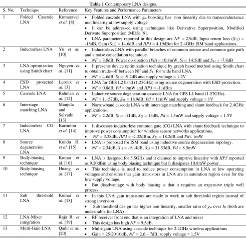
Table 1 Contemporary LNA designs. S. No. Technique Reference Key Features and Performance Parameters
1 Folded Cascode LNA
Kumaravel et al. [8]
Folded cascode LNA with gm boosting has non linearity due to transconductance non linearity at low supply voltage
It can be addressed using techniques like Derivative Superposition, Modified Derivate Superposition (MDS) [9].
LNA parameters reported in this design are NF = 2.9dB, Input return loss (S11) =
-15dB, Gain (S21) = 14.6dB and IIP3 = 4.19dBm for 2.4GHz ISM band applications.
2 Inductorless LNA Yu et al. [10]
Inductorless LNA with parallel branches of common source and common gate path and a noise cancellation technique.
NF = 3.8dB, Power dissipation (Pd) = 10.8mW, S21= 14.5dB and S11 = -7.8dB
3 LNA optimization using Smith chart
Nguyen et al. [11]
It presents device optimization technique by graph based method using Smith chart to obtain trade-off between NF and S11 for wide band LNA.
NF = 4.6dB, S11< -9.2dB and supply voltage = 1.2V
4 ESD protected LNA
Leroux et al. [3]
LNA for GPS L2 band (1.23GHz) using source degeneration with ESD protection. NF = 0.8dB, Pd = 9mW and IIP3 = -11dBm
5 Cascode LNA Rahman et al. [12]
Inductive source degeneration cascode LNA for GPS L1 band (1.57GHz). NF = 1.157dB, S21 = 18.9dB, Pd = 11mW and supply voltage = 1V
6 Interstage matching LNA
Manjula and Selvathi [13]
Narrowband cascode LNA with interstage matching and shunt feedback for 2.4GHz applications.
NF = 2.2dB, S11= -11dB, S21 = 13dB, Pd = 1.5mW and supply voltage = 1.5V
7 Inductorless CG LNA
Karimlou et al. [14]
It discusses inductorless common gate (CG) LNA with shunt feedback technique to improve power consumption for wireless sensor networks applications.
NF = 3.38dB, IIP3 = -4.32dBm, S21 = 18.2dB and Pd< 1mW
8 Source
degeneration LNA
Kundu R. et al. [15]
LNA is proposed for ISM band using inductive source degeneration topology. NF = 2.34dB, S11 = -9.14dB, S21 = 31.53dB, Pd = 8.5mW
9 Body-biasing technique
Kumar et al. [16]
LNA is designed for 5.5GHz and it claimed to improve linearity with IIP3 reported as 9.20dBm using body biasing technique but it dissipates 10.8mW power.
10 Body-biasing technique
Huang et al. [17]
This technique is used to reduce power consumption in LNA at low operating voltages and ensures that gain transistors in LNA are in saturation region even for the low supply voltage.
But disadvantage with body biasing is that it requires an expensive triple well process.
11 Sub threshold LNA
Kumar et al. [18]
In this LNA gain transistors are made to work in sub threshold region instead of strong inversion
Sub threshold design has higher non linearity, smaller ratio of gm over ID (both are undesirable for LNA)
12 LNA-Mixer integration
Raja R. et al. [19]
RF receiver front end that is an integration of LNA and mixer This design has high NF = 9.5dB.
13 Multi-Gain LNA Qadir et al. [20]
Multi-gain LNA using cascode technique for 2.4GHz wireless applications Gain = 25/20/10dB, NF = 2.6 – 7dB, supply voltage = 1.5V
from buildings, trees etc. in the physical environment) with extremely small power levels up to -130dBm (typical example of a GPS signal) [3]. CMOS design process in modern day Integrated Circuit (IC)
technology further makes the design of LNA more tedious due to reasons like addition of excess thermal noise because of presence of hot electrons in high electric fields, low transconductance and restriction in
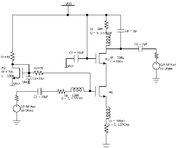
Iranian Journal of Electrical and Electronic Engineering, Vol. 15, No. 4, December 2019 446 Fig. 2 Complete circuit diagram of LNA.
voltage headroom due to scaling of CMOS devices and integration of millions of transistors on a single SoC [1, 4-8]. These design process restrictions lead to higher noise floor and affects gain and linearity of LNA as well.
There have been efforts to overcome LNA design challenges [1,3,8-21] using techniques like folded cascode design, gain boosting techniques [8], derivative superposition [9], inductive source degeneration with ESD protection [3], interstage matching [13], inductorless design [14] etc. Table 1 provides a good summary of some of the notable work in this direction while clearly bringing forth the details of the techniques used for the purpose and results obtained.
Among all the LNA design techniques brought forward in table 1, it can be inferred that circuits (mentioned at sr. no. 1,4,5,6 and 8) broadly based on inductive source degeneration topology have been found to be able to provide high gain and high reverse isolation for narrowband applications. Taking a clue from there, we in this paper report our results related to design of narrowband inductive source degeneration LNA capable of handling low power level signals specifically for GPS L1 band broadcasting at 1.57GHz with channel bandwidth of 10MHz.
Proposed LNA is simulated on Cadence Virtuoso Tool version IC6.1.6 and Spectre version MMSIM13.1 with 0.18µm technology node using generic process development kit. For source degeneration, input matching and output matching lossy inductors instead of pure inductors are used. A conscious effort has been made to improve upon the gain of the circuit by incorporating a large transistor in order to obtain higher
gm/ID ratio [6]. However, large transistors are known to suffer from losses due to higher gate resistance as well
as higher parasitic capacitances [22], which affect reverse isolation of the circuit. This problem was addressed by incorporating multiple gate fingers of narrow width in the transistor (responsible for providing gain) in present work. The total width of the transistor in the proposed design is 500µm and is implemented using 10 gate fingers with width of 50µm each. A better trade-off between NF (< 2dB) and input return loss (S11 = -29dB) is achieved using the proposed LNA
topology.
This paper has been divided in four different sections. Present section of introduction is followed by Section 2 which presents complete methodology with detailed mathematical analysis of proposed LNA that remains critical so as to calculate values of components used in the circuit design. Section 3 presents small signal s-parameters analysis, large signal analysis, Smith chart analysis along with trade-offs among different parameters of the proposed LNA under results and discussion section. Section 4 presents the conclusion of the work carried out in this paper.
2 Methodology
LNA circuit as shown in Fig. 2, which happens to be the variation of a standard inductive source degeneration topology, has been designed to obtain the value of gain in the range of 18-22dB and NF close to 2dB. It must be noted that in most circuit simulations of LNAs presented in literature, ideal inductors are considered for matching and for source degeneration. However, in the proposed design, practical lossy inductors are modelled [23] with value of quality factor (Q) equal to 5. Value of Q has been chosen on the basis of earlier reported work by Shaeffer and Lee [1].
Iranian Journal of Electrical and Electronic Engineering, Vol. 15, No. 4, December 2019 447
providing gain in the circuit but also keeping a check on the noise performance of the circuit. Gate source capacitance (Cgs) of M1 forms an input matching network with inductors - Lg and Ls. Lossy inductors have been used so as to achieve more realistic results. Circuit has been fed by RF source with 50 Ohms termination and signal power level of - 40dBm at operating frequency of 1.57 GHz. Circuit components values like inductors –Lg and Ls and W/L ratio of gain transistor M1 are calculated using Eqs. (1)–(3) so as to obtain mandatory 50 Ohms termination [24].
s m in
gs
L g Z
C
(1)
where, gm is transconductance of M1 and is given by Eq. (2) and Cgs of M1 is given by Eq. (3):
2
m n ox D
W
g C I
L
(2)
2 . . 3
gs ox
C W L C (3)
IDis drain current in M1, Cox is oxide capacitance per unit area and µn is mobility of charge carriers [6]. In
order to have high forward gain in LNA high gm/ID ratio is desired [1].
Circuit exhibits further advantage in terms of reduction of effect of Cgd, better gain, better stability and high linearity owing to usage of a cascode stage between M1 and M3. A dedicated effort has been made to propose a design of the circuit which helps in saving the chip area owing to selection of same size of M1 and M3 [25] and common usage of drain area of M1 with source area of M3.
Ld forms a parallel tank circuit with total capacitance at the output node (Cgd3, Cdb3 - gate-drain and drain-body capacitance respectively) in addition to the capacitance of the subsequent stage, assuming that there is a down converter mixer stage which would be used after LNA circuit in a real life application. An additional capacitor Cd is added in the circuit for better tuning of the tank circuit. Similar explanation of this part of the circuit has been provided earlier by [1, 5, 7].Other circuit components in Fig. 2 are coupling capacitors (C1 and C4) whose values are swept and optimized to achieve close to perfect matching at input and output ports. Capacitors C2 and C3 are used to suppress any power supply variations or noise. GPS signal occupies a
Transistor M2 forms a current mirror with transistor M1 and is responsible for setting required drain current (ID) in M1 for desired gm/ID ratio and for adequate forward gain. Drain current (I) is set in M2 by using appropriate size of M2 and current limiting resistor R1 as shown in Fig. 2. ID in M1 is obtained from Eq. (5). Resistor R2 provides high impedance connection between M2 and M1.
2 1 D
W
I
L I
W L
(5)
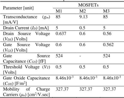
Table 2 shows the values of crucial DC parameters obtained for the proposed LNA circuit using analog simulation in Cadence Virtuoso tool. Theoretical values of gm and Cgs as obtained from Eqs. (2) and (3), respectively, are very close to their simulation values listed in Table 2. This indicates that adequate gm/ID is available in the circuit to have desired gain and parasitic capacitances (Cbd and Cgd) are extremely small.
Theoretical values of Lg and Ls differ from their practical values in the design. This is due to the fact that in theoretical analysis only Cgs of MOSFET is considered and Cgd and Cbd, that are small values in comparison to Cgs, are ignored. Also theoretical values of components are calculated considering the perfect match condition (i.e. impedance of RF source and load is equal to 50Ohms). Implementation of the design on Cadence Virtuoso tool was started with theoretical
Table 2 DC parameters.
Parameter [unit] MOSFETs
M1 M2 M3
Transconductance (gm) [mA/V]
85 9.13 85
Drain Current (ID) [mA] 5 0.5 5 Drain Source Voltage
(VDS) [Volts]
0.637 0.6 0.56
Gate Source Voltage (VGS) [Volts]
0.6 0.6 0.562
Gate Source
Capacitance (CGS) [fF]
524 - 524
Threshold Voltage (VT) [Volts]
0.5 0.5 0.5
Gate Oxide Capacitance (COX) [F/m2]
8.46x10⁻³ 8.46x10⁻³ 8.46x10⁻³
Mobility of Charge Carriers (μn) [cm2/V.sec]
327.37 327.37 327.37
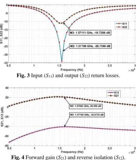
Iranian Journal of Electrical and Electronic Engineering, Vol. 15, No. 4, December 2019 448 Fig. 3 Input (S11) and output (S22) return losses.
Fig. 4 Forward gain (S21) and reverse isolation (S12).
values of inductors Lg and Ls. Their values were swept in the design to get desired small signal s-parameters first and then large signal linearity parameters.
3 Results and Discussion
Having explained the design part of LNA circuit under consideration in the Methodology section, present section of Results and Discussions summarizes all the obtained results and discuss the same in light of already reported work. Simulations of the proposed LNA circuit are carried out using Spectre simulator version MMSIM13.1 [26].
3.1 Small Signal S-Parameters Analysis
S-parameter analysis is carried out to linearize the circuit about DC operating point by applying a small test signal with the power level of -40dBm at 1.57GHz. Fig. 3 shows the plot for S11 and S12 against variation of
frequency from 500MHz to 3GHz. It can be clearly observed that a dip in the values of S11 and S22 in the
plot is observed in a narrow band at the frequency of interest, i.e. 1.57GHz. Although the values of both S11
and S22 are found to be below 0dB for a broader range
of frequency, the same fall to -29dB and -10.72dB respectively over the operating frequency of 1.57GHz. This clearly indicates that we have been able to establish good matching at both the input and output ports.
Performance of LNA circuit is further verified by finding out the results for forward gain (S21) and reverse
isolation (S12) as shown in Fig. 4. While S21 is constant
for a range of frequencies, the peak value of 21dB is found at 1.57GHz. Similarly S12 which is indicative of
Fig. 5 Noise figure.
Fig. 6 Plot of stability test (K-∆).
leakage power from output to input is constant over a range of frequencies but is observed to possess the lowest value equal to -41dB at frequency under consideration. It indicates very small leakage power from output back to input at operating frequency. High gain and good reverse isolation is due to good input and output matching in the circuit.
Another important parameter, which must be taken into consideration for design of LNA is noise figure (NF). Accurate estimation of the same becomes even more important as NF of LNA gets added directly to the total NF of the RF receiver [5]. Fig. 5 depicts a measure of NF over a broader range of frequency from about 0.5GHz to about 3GHz. As can be clearly seen that NF is observed to be almost constant from 500MHz to 1.57GHz and then rises sharply, NF of 1.98dB is obtained at 1.57GHz in the proposed design. Some of the earlier published works [8, 10, 13-16, 20] have also reported NF in the range of about 2 to 3dB for the LNAs using inductive source degeneration topology. Noise in the LNA circuit exist due to losses caused by gate resistance and due to parasitic capacitances primarily dominated by Cgs, Cgd, and Cdb of the main transistor (responsible for gain) in the circuit. In the proposed design effect of gate resistance is mitigated by using narrow gate fingers and effect of parasitic capacitances is addressed with optimum matching using inductors at input and output ports. Cascode configuration in the circuit also plays a vital role in removing Miller effect caused by Cgd in the circuit.
We have also calculated the theoretical value of NF
using Eqs. (6) and (7) [1].
Iranian Journal of Electrical and Electronic Engineering, Vol. 15, No. 4, December 2019 449 Fig. 7 Plot of GT, GA and GP. Fig. 8 Plot of GUMAX and GMAX.
(a) (b) (a) (b)
Fig. 9 a) Plots of GACs, and b) Plot of NCs. Fig. 10 a) Plot of optimum GAC and NC, and b) S12, S11 and S22
plots on Smith chart.
2
1 5.6 T
NF
(6)
m T
gs
g
C
(7)
ωT is carriers’ transition frequency in short channel MOSFET and ω is operating frequency of LNA. Value of NF calculated this way theoretically is quite in agreement with the values observed from simulation. Further, it remains of paramount importance to check the performance of the proposed LNA circuit for stability. For that, a small signal stability test of the circuit i.e. K-delta test is performed. Results of the same have been shown in Fig. 6. K is greater than 1 for a range of frequency (1–3GHz) and ∆ is less than 1 therefore circuit is unconditionally stable for a range of frequencies.
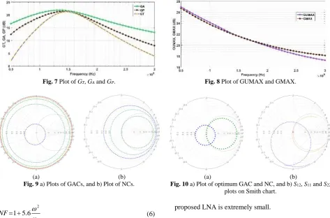
Fig. 7 is a plot of transducer gain (GT), operating gain (GP) and available gain (GA) for the proposed LNA circuit. Theoretically GA>GP>GT [24] and same result is obtained from the plot. Also, at the frequency of operation all three gains are equal i.e. GA = GP = GT, this indicates almost perfect input and output matching in the proposed LNA at 1.57GHz.
Maximum unilateral transducer gain (GUMAX) is LNA gain when S12 = 0 and LNA is conjugately
matched to source and load (i.e. Γs = Γ*in = S*11 and ΓL =
Γ*
out = S*22) [24]. Maximum Gain (GMAX) is LNA gain
when S12 is not zero but is an extremely small value.
Closeness of GUMAX and GMAX as shown in Fig. 8, plot of GUMAX and GMAX asserts that S12 of the
proposed LNA is extremely small.
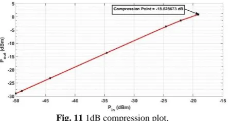
3.2 Graphical Analysis Using Smith Chart
Graphical analysis of LNA S-parameters using Smith chart is done to understand the trade-offs between
design parameters and to optimize them.
References [11] and [27] have used Smith chart method for optimization of LNA. Both GA and NF of LNA are function of source reflection coefficient (Γs) [24],
therefore available gain circle (GAC) and noise circle (NC) is plotted on Smith chart of Γs. Fig. 9(a) is a
plot of GACs (co-centric circles) for different values of gain at frequency of interest. Circle with the smallest radius (blue circle) corresponds to maximum gain which is 21dB for the proposed design. Center of this circle corresponds to value of Γs. Ideally center of GAC
should lie at the center of smith chart (where Γs = 0),
practically it should be close to the center of smith chart and is equal to S*
11 (conjugate match i.e. Γs = S*11). As
can be seen from the plot in Fig. 9(a) center of GAC lies very close to center of smith chart which is an indication of near perfect input match. Similarly, Fig. 9(b) is plot of NCs for different values of NF. Circle with smallest radius (green color) corresponds to minimum NF which is < 2dB and center of this circle corresponds to value of Γs for most optimum NF. Fig. 10(a) is a plot of most
optimum GAC (blue circle) and NC (green circle), their centers do not coincide which is indicative of a fact that there is a trade-off between Gain and NF. However for optimum design both centers should lie close to the center of Smith chart.
S12 of LNA should be extremely small as it is obtained
Iranian Journal of Electrical and Electronic Engineering, Vol. 15, No. 4, December 2019 450 Fig. 11 1dB compression plot.
in the proposed design and should lie close to center of Smith cart. S11 and S22 should also lie close to center of
Smith chart. Fig. 10 (b) is S12, S11, and S22 plots on
Smith Chart. S12 is a purple color dot, which lies exactly
at the center of Smith chart. S11 traces orange color
curve in the figure. It indicates value of S11 at different
frequencies. At 1.57GHz, S11 is 0.018+j0.084 with
normalized input impedance of LNA at this point equals 0.98+j0.16 (very close to the center of smith chart). Similarly S22 traces blue color curve and at 1.57GHz, its
value is 0.12+j0.249 with normalized output impedance equal to 1.11+j0.60.
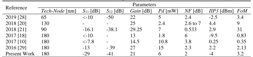
3.3 Large Signal Analysis
Linearity of LNA is measured using large signal analysis that gives range of input signal power levels that could be amplified by LNA without causing intermodulation, compression, and blockage of adjacent channels. Linearity is measured using 1dB compression point and Input Intercept Point3 (IIP3). Fig. 11 is plot of 1dB compression point in the proposed LNA found to be equal to -18.6dBm which is quite sufficient for this design as GPS signal power is always below -40dBm. In the proposed LNA for GPS L1 band, channel bandwidth is 10MHz. Two adjacent channels –ω1 and ω2 produce
3rd order intermodulation components
–
2ω 1±ω2,2ω2±ω1 due to non-linearity of the circuit. IIP3 is a
hypothetical point as shown in plot in Fig. 12 where 3rd
order power gain line of intermodulation component intersects with fundamental frequency power gain line.
IIP3 of proposed LNA is -4dBm and is a measure of linearity of LNA. Theoretically it should be at least 10dBm above 1dB compression point.
3.4 Comparative Analysis
Table 3 shows the comparison of LNA proposed in this paper with the ones already existing in the literature.
Comparison has been made with some of the very recent work published by Abdelhamid et al. [28], Qadir
et al. [20] ,Yadav et al. [21], Kumar et al. [18], Yu
et al. [10] and Safari et al. [29] respectively. While Abdelhamid et al. [28] have used a 65 nm technology node to design LNA circuit, Qadir et al. [20] and Yadav
et al. [21] have used 130 nm and 90 nm technologies,
Fig. 12 IIP3 Plot.
respectively. Kumar et al. [18], Yu et al. [10] and Safari
et al. [29] have used 180 nm technology node. Value of
S11 is reported to be -29dB in the present paper which is
found to be the least among contemporary LNA designs. While Yadav et al. [21] have reported the highest value of gain of the order of 29.25dB using 90 nm technology node, but the power drawn is higher than the value reported in the present work. Further, the value of gain reported in this work is comparable to Abdelhamid et al. [28] that too with better values of noise figure. S12 value reported by Abdelhamid et al.
[28] stands out to be the best (-50dB). In the present work S12 is reported as -41dB which is better than all the
other designs compared in table 3. Value of power dissipation reported in this work equal to 6mW is also quite optimum and is comparable to the rest of the topologies. Overall, it is found that the circuit presented in this work is quite optimized to obtain a reasonably good combination of all the parameters viz. S11, S12,
Gain, Pd, NF and IIP3 in comparison to some of the latest works in this field. In addition, figure of merit (FoM) for all six LNA designs compared with the present work is calculated using Eq. (8) [30] and it has been found that FoM of present work is quite comparable with already existing designs.
-1 abs
mW
abs 1 . mW
Gain FoM
NF Pd
(8)
Results obtained here may go a long way in giving further direction to design of next generation of LNA circuits for dedicated applications.
Development of dedicated models for various electronic components (both active and passive) and their usability in millimeter wave applications will be the subject matter of future course of research by us.
4 Conclusion
Narrowband LNA using inductive source
degeneration topology is designed for GPS L1 band application broadcasting at 1.57GHz. Inductors with quality factor to model the losses are used for better tuning and matching in the design. Detailed analysis is carried out and all the DC parameters are reported. Smith chart analysis of results is presented that helped
Iranian Journal of Electrical and Electronic Engineering, Vol. 15, No. 4, December 2019 451
in understanding the trade-offs and it also facilitates fast optimization. The proposed LNA is compared against several contemporary narrowband LNAs designed using same inductive source degeneration topology and on several parameters including S11, S12, Gain and NF.
Acknowledgements
Thanks are due to Cadence Online support for addressing important queries regarding the tool, for support in setting up important model libraries and for making available important literature pertaining to RF design using Cadence Virtuoso and Spectre tool. Mr. Ashish Patni - Staff Support Applications Engineer, Cadence, Noida was point of contact and he addressed authors’ queries. Authors of this work were also benefited from video lectures on RF design offered by Dr. Susanta Sengupta through Indira Learning. At some point during the research work authors corresponded with Dr. Sengupta and took his valuable technical help on RF design issues. Thanks are also due to Mr. Kulbhushan Sharma, PhD Scholar, Chitkara University for his support in plotting the graphs in MATLAB from CSV files generated from Cadence tool.
Overall, authors deeply acknowledge the support received from Chitkara University in establishing the necessary infrastructure which made it possible to carry out this research work.
References
[1] D. K. Shaeffer and T. H. Lee, “A 1.5-V, 1.5-GHz CMOS low noise amplifier,” IEEE Journal of Solid-State Circuits, Vol. 32, No. 5, pp. 745–759, 1997.
[2] T. H. Lee, The design of CMOS radio-frequency integrated circuits. Cambridge University Press, 2003.
[3] P. Leroux, J. Janssens, and M. Steyaert, “A 0.8-dB NF ESD-protected 9-mW CMOS LNA operating at 1.23 GHz,” IEEE Journal of Solid-State Circuits, Vol. 37, No. 6, pp. 760–765, 2002.
[4] C. Y. Cha and S. G. Lee, “A 5.2 GHz LNA in 0.35µm CMOS utilizing inter–stage series resonance and optimizing the substrate resistance,” in 28th European IEEE Solid-State Circuits Conference (ESSCIRC), Florence, Italy, pp. 339–342, 2002.
[5] B. Razavi, RF microelectronics. 2nd Edition. New
Jersey, Prentice hall, 2012.
[6] R. J. Baker, CMOS: Mixed-signal circuit design. John Wiley & Sons, 2008.
[7] H. Fouad, K. Sharaf, E. El-Diwany, and H. El-Hennaway, “An RF CMOS modified-cascode LNA with inductive source degeneration,” in 19th
National IEEE Radio Science Conference,
Alexandria, Egypt, pp. 450–457, 2002.
[8] S. Kumaravel, A. Kukde, B. Venkataramani, and R. Raja, “A high linearity and high gain folded cascode LNA for narrowband receiver applications,”
Microelectronics Journal, Vol. 54, pp. 101–108, 2016.
[9] V. Aparin and L.E. Larson, “Modified derivative superposition method for linearizing FET low-noise amplifiers,” IEEE Transactions on Microwave Theory and Techniques, Vol. 53, No. 2, pp. 571– 581, 2005.
[10]Y. Yu, K. Kang, Y. Fan, C. Zhao, H. Liu, Y. Wu, Y. L. Ban, and W. Y. Yin, “Analysis and design of inductorless wideband low-noise amplifier with noise cancellation technique,” IEEE Access, Vol. 5, pp. 9389–9397, 2017.
[11]G. D. Nguyen, K. Cimino, and M. Feng, “A RF CMOS amplifier with optimized gain, noise, linearity and return losses for UWB applications,” in
Radio Frequency Integrated Circuits Symposium, Atlanta, GA, USA, pp. 505–508, 2008.
[12]S. I. Rahman, S. A. Kareem, and S. Habeeb, “Design of a low noise amplifier using 0.18 µm CMOS technology,” The International Journal of Engineering & Science, Vol. 4, pp. 11–16, 2015.
[13]S. Manjula and D. Selvathi, “Design of low power 2.4 GHz CMOS cascode LNA with reduced noise figure for WSN applications,” Wireless Personal Communications, Vol. 70, No. 4, pp. 1965–1976, 2013.
[14]A. Karimlou, R. Jafarnejad, and J. Sobhi, “An inductor-less sub-mw low noise amplifier for wireless sensor network applications,” Integration - The VLSI Journal, Vol. 52, pp. 316–322, 2016.
[15]R. Kundu, A. Pandey, S. Chakraborty, and V. Nath, “A CMOS low noise amplifier based on common source technique for ISM band application,”
Microsystem Technologies, Vol. 22, No. 11,
pp. 2707–2714, 2016.
Iranian Journal of Electrical and Electronic Engineering, Vol. 15, No. 4, December 2019 452
“Design of 5.5 GHz linear low noise amplifier using post distortion technique with body biasing,”
Microsystem Technologies, Vol. 22, No. 11,
pp. 2681–2690, 2016.
[17]M. Y. Huang, R. Y. Huang, and R. M. Weng, “A 0.3V low cost low power 24GHz low noise amplifier with body bias technology,” in IEEE
Computer Society Annual Symposium, Bochum,
Germany, pp. 519–522, 2017.
[18]A. A. Kumar, B. D. Sahoo, and A. Dutta, “A wideband 2-5 GHz noise cancelling subthreshold low noise amplifier,” IEEE Transactions on Circuits and Systems II: Express Briefs, Vol. 65, No. 7, pp. 834–838, 2017.
[19]R. Raja, A. A. Kukde, and B. Venkataramani, “A low power fully differential RF receiver front-end for 2.4 GHz wireless sensor networks,” Microsystem Technologies, Vol. 25, No. 5, pp. 1809-1822, 2019.
[20]M. W. Qadir, M. H. Memon, A. F. Mirza, S. W. Ali, and F. Lin, “Multigain cascode technique for low power BLE ISM band 2.4GHz differential inductive source degeneration based LNA,” in IEEE
MTT-S International Wireless Symposium (IWS),
Chengdu, China, pp. 1–4, 2018.
[21]N. Yadav, M. J. Khan, J. Singh, A. Pandey, M. Kumar, V. Nath, and L.K. Singh, “A 0.533 dB noise figure and 7 mW narrowband low noise amplifier for GPS application,” Lecture Notes in Electrical Engineering, Springer, Vol. 453, pp 305-315, 2018
[22]C. H. Doan, S. Emami, A. M. Niknejad and R. W. Brodersen, “Millimeter-wave CMOS design,” IEEE Journal of Solid-State Circuits, Vol. 40, No. 1, pp. 144–155, 2005.
[23]Creating a Parameterized Cell in Cadence, Tutorial,
June 2013. [Online]. Available:
https://wikis.ece.iastate.edu/vlsi.
[24]R. Ludwig, RF circuit design: theory & applications. 2nd Edition, Pearson Education India,
2000.
[25]C. Zhang, D. Huang, and D. Lou, “Optimization of cascade CMOS low noise amplifier using inter-stage matching network”, in IEEE Conference on Electron
Devices and Solid-State Circuits, Hong Kong,
China, pp. 465–468, 2003.
Accelerated Parallel Simulator RF Analysis, User
Guide, March 2016. [Online]. Available:
https://www.cadence.com.
[27]K. G. McCarthy, “An educational tool for RF LNA analysis based on an implementation of the Smith chart in excel,” in IET Irish Signals and Systems Conference (ISSC), Maynooth, Ireland, 2012.
[28]A. A. Abdelhamid, M. T. Ozgun, and H. Dogan “A fully integrated 2.4 dB NF capacitive cross coupling CG-LNA for LTE band,” Analog Integrated Circuit and Signal Processing, Vol. 99, No. 1, pp. 159–166, 2019.
[29]M. Safari, M. Eghtesadi, M. R. Mosavi, “A concurrent dual-band low noise amplifier for GNSS receivers,” Iranian Journal of Electrical and Electronic Engineering, Vol. 12, No. 2, pp. 119-125, 2016.
[30]D. Linten, L. Aspernyr, W. Jearnsaksiri, J. Ramos, A. Mercha, S. Jensi, S. Thijs, R. Garcia, H. Jacobsson, P. Wambacq, and S. Donnay, “Low-power 5 GHz LNA and VCO in 90 nm RF CMOS,” in Proc. Symposium on VLSI Circuits, Honolulu, USA, pp. 372–375, 2004.
S. Juneja is working as Research Associate at Chitkara University, India. He completed his M.E. in Electronics & Communication (ECE) Engineering from Chitkara University, India and B.E. (ECE) from Punjab Technical University. He has 5 years of industry experience working in Texas Instruments, India and RS Components, India. His research interests include analog design, mixed signal design and embedded systems design. He has published his work in IEEE & Springer Conferences and has filed 6 patents in Indian Patent Office (IPO).
R. Sharma earned his PhD from National Physical Laboratory, New Delhi and served in Birla Institute of Technology and Science (BITS), Pilani as a Faculty for 6 years. He has been a visiting scholar at Purdue University, USA and has more than 35 research papers in international journals and conferences of repute. Besides this, he has been a co-author of a text book on ‘Solid State Electronic Devices’ published by Oxford University Press. He is a senior member of IEEE and holds current interest in the broad field of microelectronics while focusing on contemporary electronic devices and analog circuits for applications related to neural amplifiers & RF.
© 2019 by the authors. Licensee IUST, Tehran, Iran. This article is an open access article distributed under the terms and conditions of the Creative Commons Attribution-NonCommercial 4.0 International (CC BY-NC 4.0) license (https://creativecommons.org/licenses/by-nc/4.0/).