Printed in The Islamic Republic of Iran, 2014 © Shiraz University
DESIGN AND IMPLEMENTATION OF PRECISE HARDWARE FOR
ELECTRICAL IMPEDANCE TOMOGRAPHY (EIT)*
M. KHALIGHI1** , B. VOSOUGHI VAHDAT2, M. MORTAZAVI3 AND M. MIKAEILI4 1School of Engineering and Science, Sharif University of Technology, International Campus, I. R. of Iran
Email: [email protected]
2School of Engineering and Science, Sharif University of Technology, Tehran, I. R. of Iran 3School of Engineering, Islamic Azad University-Abhar Branch, I. R. of Iran
4Dept. of Engineering, Biomedical Engineering Group, Shahed University, Tehran, I. R. of Iran
Abstract– Electrical Impedance Tomography (EIT), is one of the safest medical imaging technologies and can be used in industrial process monitoring. In this method, image of electrical conductivity (or electrical impedance) distribution of the inner part of a conductive subject can be reconstructed. The image reconstruction process is done by injecting an accurate current into the boundary of a volume conductor (Ω), measuring voltages around the boundary (∂Ω) and transmitting them to a computer, and processing on acquired data with software (e.g. MATLAB). The image would be reconstructed from the measured peripheral data by using an iterative algorithm. A precise instrumentation (EIT hardware) plays a very important and vital role in the quality of reconstructed images. In this paper, we have proposed a practical design of a low-cost precise EIT hardware including, a high output impedance VCCS (Voltage-Controlled Current Source) with pulse generation part, precise voltage demodulator and measuring parts, a high performance multiplexer module, and a control unit. All the parts have been practically and accurately tested with successful results, and finally the proposed design was assembled on PCB. The quality of experimental results at the end of this paper, (reconstructed images by using the implemented system), confirms the accuracy of the proposed EIT hardware.
Keywords– EIT, electrical impedance tomography, EIT hardware, EIT instrumentation, EIT currentsource
1. INTRODUCTION
Electrical Impedance Tomography (EIT) is a relatively new imaging technique. In this method, an image of the inner part of a conductive domain (Ω) can be made with an array of external electrodes which are located on the boundary of domain (∂Ω). In this imaging method, the image of electrical conductivity (or impedance) distribution of the internal part of a typical conductive subject can be reconstructed [1]. EIT procedure includes injecting an accurate current into the boundary of domain (∂Ω) via a pair of electrodes, measuring the boundary voltages by means of other electrodes around the boundary and transmitting them to a computer, and at the end, processing the acquired data with software (e.g. MATLAB) to reconstruct the image. Human body tissues contain a wide range of conductivities, and hence the potential exists to use EIT to carry out medical imaging using the conductivity as the parameter to be mapped [2].
As a matter of fact, EIT is a challenging problem. This technique has some advantages compared to other methods, including: simplicity of application, no hazard to the patient (such as X-ray), low cost and portable, and the high speed of data collection and image reconstruction [3]. Although EIT systems suffer
from poor im of unknown quality [4]. algorithms t most impor Reconstruct algorithm [7 This pa design is ill that, some e end, final re
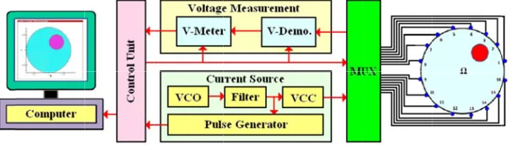
In general, E EIT-sensors iterative alg data acquisi The precisio proposed EI different pa 1- VCCS a VCC 2- Multip 3- Contro 4- Voltag The co (∂Ω) via th types of pu waveform. demodulatio the electrod block. Cont communica mage resolut n skin–electr
EIT still has to reconstruc rtant of them ted image q 7].
aper is focus lustrated and experiments econstructed
EIT instrum s and a PC. gorithm. In o ition part (to on of all uni IT system is arts: (Voltage-Co C (Voltage-to plexer modul ol unit. ge measurem
onstant and a he multiplexe ulse train sim They can be on portion. I des voltage, “ trol unit is ap ating with the
tion, the tran rode impedan
s technical d ct the image m is hardwar
quality main
sed on hardw d explained,
done by usi image of ou
Fig. 1.The ma
2. TO
entation com The image i ur design, th o measure vo its plays a ve illustrated in
ontrolled Cu o-current con
e.
ent part cont
accurate curr er part (MU multaneous w
e used for sa In order to m “V-Demo.” a pplied for co e PC for data
nsfer impedan nce on measu difficulty in t
s. However, re improvem nly depends
ware implem and each pa ing the imple ur EIT system
ain block diag
OP VIEW O
mprises digita is finally rec he analog sec oltages with ery importan n Fig. 1. The
urrent Source nverter) part,
taining a volt
rent produce UX). The sec with maximu ampling of re measure the and “V-Mete ontrolling the a transaction.
nces must st urement erro terms of dev there are so ments to acq on the bou
mentation of E art of the des emented syst m will be com
gram of propo
OF PROPOS
al and analog constructed f ction of hardw
enough prec nt role in rec
e block diagr
e) which incl and a pulse
tage demodu
ed by the VC cond task of um point of eal and imag boundary vo er” blocks sh e multiplexer . The assemb
ill be measur ors can also h veloping hard ome methods quire a high-undary data
EIT. First of sign will be tem and thei mpared with
sed EIT hardw
SED DESIG
g circuits, an from the acq ware include cision). The onstructed im ram of the pr
udes a VCO generator.
ulator and a v
CCS is injec f the current positive pea ginary section
oltage, mean hould be app
r module an bled EIT hard
red with high have a signif dware for da s to improve -accuracy me
accuracy an
f all, the top described in ir results wil
other works.
ware design
GN
n array of ele quired data ( es an accurat digital part mage quality roposed EIT
O as a wavefo
voltmeter.
cted into the source sect aks and zero ns of measur ning demodu plied respecti d measurem dware is sho
h accuracy. T ficant effect ata acquisitio e imaging qu easured datu nd the recon
view of our n detail as w ll be presente .
ectrodes whi voltages) by te current sou
contains con y. The top vi
hardware (F
orm generato
e boundary o ion is gener points of th red voltage i ulating and m ively after m
ent parts, an wn in Fig. 2
The effect on image on and the uality. The um [5, 6]. nstruction
proposed well. After ed. At the
ich acts as y using an urce and a ntrol unit. iew of the Fig. 1) has
or, a filter,
of domain rating two he current in voltage measuring multiplexer nd also for
Electrical Im frequency r current is to positive and VCCS used parts. Desig precision, w systems in m digital or an output wave ideal voltag addition, th impedance, range of lo source can a
The cu 10KHz and must be in t satisfy the a (Voltage-Co filters in ser
a) Wavefor
Schema (EXAR Inc
mpedance T range and wit
o use a volta d negative fe d in the EIT s gn of the VC which means
most cases i nalog form [ eform (i.e. ex ge source), w he main chara
linearity in oad, and prop ameliorate th urrent source d 1MHz and the range of above condit ontrolled Os rial connectio
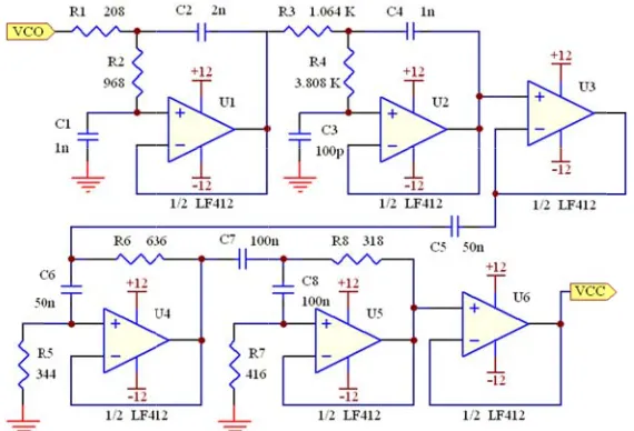
rm generatio
atic circuit o .) has been u
3. VOLTA
omography th a large va age-controlle eedback arou systems, con C in EIT sys that it must is the sinusoi [9]. The main
xact sinusoid wide operatio acteristics fo converting per working he image qua in EIT syste be able to s more than 10 tions. Figure scillator) part on), and a VC
Fig ion
of the wavef used in the w
Fig. 2. Ass
AGE-CONTR
(EIT) system ariation in loa ed current so und a high g nsists of wav stems is espe have high ou idal wavefor n features fo dal waveform onal bandwid or the VCC p voltage to c g in a broad ality to a cert ems must be support the 00KΩ as we e 3 shows th t, a Butterwo CC (Voltage
g. 3.Flowchar
form generat waveform os
sembled EIT h
ROLLED C
ms require ac ad impedanc ource (VCCS
ain operation veform gener
ecially impor utput impeda rm which is or a typical w m without any dth, and stea
part to have current, prec d range of fr tain extent [1 able to deliv load betwee ell [12], there he flowchart orth band-pa e-to-Current
rt of proposed
tion part is s scillator part
hardware
CURRENT S
ccurate curre ce. The simp S), which ca nal or instrum rator and Vo
rtant. The VC ance. Genera
produced by waveform ge y jitter), a lo ady amplitud an excellen ision of outp requency [10 11].
ver the curren en 100Ω and
efore an exce of the propo ass filter (Bu
Converter) p
VCCS design
shown in Fig t as a VCO.
SOURCE
ent sources t lest techniqu an be defined
mentation am ltage-to-Curr CC part requ ally, the wav y the wavefo enerator are a w output imp de over all th nt VCCS are put wavefor 0]. The high
nt over a freq d 10KΩ [9].
ellent current osed VCCS. utterworth lo part.
n
g. 4. As it c An AD844
that work ov ue to obtain a
d as a comb mplifier [8]. rent Convert uires stability eform used i orm generati
as follow; an pedance (sim he frequency
based on hi m, supportin h-performanc
quency range Its output im t source desi
It consists o ow-pass and
can be seen, IC has been
ver a wide a constant ination of A typical ter (VCC) y and high in the EIT on part in n accurate milar to an range. In igh output ng a wide ce current
e between mpedance gn should of a VCO high-pass
the output o value at th AD844, is a
b) Butterw
In orde output impe 250KHz, ha operational design the f circuit of th pass filter ( filter (U4 an
of the VCO, e output of about 690Ω a
worth band-p
er to have an edance for th as been desi
frequency r filter for othe he filter is sh
(U1 and U2)
nd U5) with a
Fig. 5. Bu
, to amplify f waveform
and with this
Fig. 4. Voltag pass filter
n exact wav he next stage igned and pl range of the er frequencie own in Fig. with cutoff a cutoff frequ
utterworth Ba
the sinusoid generation p s IC, is about
ge-controlled
veform witho e (VCC), a B laced betwee
designed EI es, the Butter
5. As it is sh frequency o uency of 10 K
and-pass filter
dal waveform part (measur t 14Ω).
oscillator (wa
out any jitter Butterworth en the VCO IT system w
rworth coeff hown, the filt f 250 KHz a KHz that are
r which is put
m and also t red output i
aveform gener
r, noise and band-pass fi and VCC p ould be betw ficients have
ter consists o and also a fo connected s
between the V
to create a l impedance o
ration part)
distortion, a ilter Ranging parts of curre ween 10 and been cited i of a fourth-o ourth-order B serially.
VCO and VCC
ow output im of the circui
and also to c g between 10
ent source. H d 250KHz. In n [13]. The s rder Butterw Butterworth
C parts
mpedance it without
create low 0KHz and Hence the n order to schematic worth
c)
Voltage-The en were done configuratio
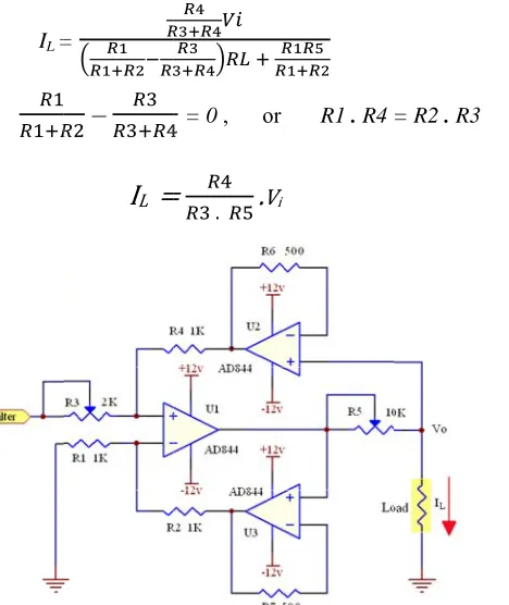
VCCS
VCCS
VCCS
VCCS
These values such According t modified. T operational schematic c PSPICE), a components TOA1 circu
Here, if:
We can get
:
The ou 7, V1 repres
measured o optional val an oscillosc
-to-current c
nd structure o to improve ons of a VCC S based on A S based on D S based on T S based on T
experiments h as different to results of The main se
band-width circuits of d and their resu s value, acco uit, (2) should
:
Fig. 6.P
utput impeda sents the me output voltag lue [2]. In or cope, the inpu
converter
of mentioned e and modi CS:
AH (Advance DOA (Double OA1 (Triple OA2 (Triple
s were done t resistance v f the primary elected crite h, and the m different VC
ults have bee ording to the d be satisfied
IL =
Proposed struc
ance Zout of a
easured outp ge of R1, wh
rder to measu ut impedance
d flowchart i fy its opera
ed Howland) e-Operationa e-Operationa e-Operationa
with identic values, diffe y practical te eria in the p minimum an CSs which en shown in e best result d and therefo
=
–
I
Lcture of the VC
a typical curr put voltage o en S is close
ure the outpu e of the voltm
is Voltage-to ation. Sever
, [14, 15]. al Amplifier)
l Amplifier f l Amplifier f
cal VCOs, d rent types o ests, the bes primary tests nd maximum
have been u Appendix A t in experime ore IL is calcu
= 0 , or
. .Vi
CC section, w
rent source c of R1, when
ed. RP and R
ut impedance meter (oscillo
– ∙
o-Current con ral essential
, [16]. form 1), [17] form 2), [9].
different VCC f OP-AMP, t structure o s were base m loads tha used in prac A. Proposed s
ents is show ulated by (3)
R1 . R4 =
with suggested
can be calcul the switch S R1 are conne
e and also loa oscope) shou
nverter (VCC tests were
].
C structures, and also dif of the VCC p ed on the ou at each VCC ctical tests a
structure of wn in Fig. 6.
).
= R2 . R3
components v
lated by (4).
S is opened
ected at the ad voltage of uld be consid
C), many exp done on f
, different co fferent range
part was sel utput imped CS can supp and simulati
the VCC par For VCCS
values
As it is show and V2 repre
output of VC f a typical V dered.
periments four main
omponent es of load. lected and dance, the port. The ons (with rt with its
based on
(1)
(2)
(3)
wn in Fig. esents the CCS with VCCS with
Figure to the circu which the V be exact sin during the t Impedance particular fr in Fig. 8A. resistor, wh
Fig. 8. (A) Th VCCS, in di output voltag with PSPICE
8A shows th uit of Fig. 6. VCCS can su nusoid and t test. The amp
of a current requency is a
The best va hich creates h
he curve repre fferent freque ge of impleme E in different f
Fig. 7.A m
he results of In the curve upport in a sp the relationsh plitude of lo t source dep also restricte lue for R1 to
higher output
esents the ran encies and dif ented VCCS i frequencies
method for mea
f other practic e, Maximum
pecific frequ hip of the in oad current w
ends on inve d by the valu o R4 was sele
t impedance
nges of maxim fferent values in different fre
asuring VCCS
cal tests to d m allowable l uency. The o nput voltage was adjusted erse of frequ ue of output ected as 1KΩ
compared to
mum allowable of R1 to R4 a equencies. (C
S output imped
determine the load represen output wavefo
of VCC par on 1mA in uency [9]. T impedance.
Ω. This is du o others.
e load which c according to t
) Output Impe dance [2]
e best value nts the maxim form of VCC
rt and load c all frequenci The maximum
As a result a ue to the VC
can be suppor the circuit in edance of pro
for R1 to R4
mum value o CS (load volt
current must ies. In fact, t m allowable according to C structure w
rted by the im Fig. 6. (B) O oposed VCCS,
according of load in age) must t be linear the output load in a the curve with 1KΩ
With t which decre was tested AMPs were this part the circuit (open of simulated
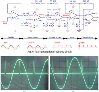
d) Pulse ge
A puls types of syn current wa demodulatin diagram. Th of the pulse pulse width pulse train voltage in th
The data ac voltage acq
this resistanc eases to abou
with resistor e heated up. T
e output volt n circuit volt d VCCS in P
enerator
e generation nchronous pu aveform (pe
ng the bound he input of th es with R2. A
h can be vari and also the he demodula
Fig.
cquisition sy quiring parts
ce value the ut 8KΩ in 2 rs less than The result of tage of the V tage), in ope PSPICE.
n module has ulse train wi ak detection dary voltages he pulse gene As shown in F ied by increa e signal of P ator section.
F
10. The outpu
4
stem can lim s of the EI
maximum a 250KHz as sh
1KΩ (~0.5K f the other pr VCCS was m erational freq
s been attach ith the maxim n and zero s in order to erator is conn Fig. 10, secti asing C1 from
oint B may
Fig. 9. Pulse ge
ut generated pu
4. VOLTAG
mit the overa IT system. R
allowable loa hown in the KΩ), howev ractical test f measured wh quency range
hed to the V mum point o
detection measure the nected to the ions A and B m 1nF to 10
be used for
eneration sche
ulses. (A) Peak
GE MEASUR
all accuracy Related to
ad in freque upper curve ver, the wave for the propo hen there wa e. Part C of F
VCCS circui of positive pe
of the curr em. Figure 9 e output of th B depict the w
nF. For insta sampling an
ematic circuit
k detection (B)
REMENT
[18]. Errors the topology
encies less th e of Fig. 8A
eform was d osed VCCS is asn’t any loa Fig. 8 shows
t design in o eaks and zer rent).The pu 9 shows the p he filter. We worthwhile u ance, by reg nd extracting
) Zero detectio
arise from b y that is ap
han 100KHz . The circuit distorted and
s shown in F ad at the outp
the output im
order to gen ro points of t ulses were pulse generat may shift th usage of this gulating R2, t
g real part o
on
both current pplied for m
z is 12KΩ
t in Fig. 6 d the OP-Fig. 8B. In
put of the mpedance
nerate two the output used for tor circuit he position s part. The the output f the load
(measuring addition to are connecte
a) Demodu
In orde stage, the vo for measure should be t positive pea to the 90 d known as p [19].
As it i buffers are entered via part of the l port D must works as th amplifier) a those menti [20]. To me pulse should
pattern) in e avoiding me ed to the cur
ulation of ele
er to measure oltage demo ement. As an taken from t ak. On the m degree phase pulse-sample
is shown in entered to th ports C and load voltage t be connecte he peak dete are the demo ioned voltage
easure the im d be applied
R7 = R
each momen easurement e rrent source i
ectrodes volt
e the bounda dulator samp n example, i the load volt mentioned po shift. The m demodulatio
Fig. 11, bo he high spee
D, come fro e, port C mu
ed to the max ector). Henc odulated elec es. The gain maginary pa
as well.
R8
Fig. 11. Prop
nt, only one rror because is not measur
ltage
ary voltage, a ples the volta in order to m tage when th oints, the vol
method of m on. The sugg
th electrode ed CMOS-lo om the pulse st be connec ximum point e the input trode voltag value determ art of the loa
osed design fo
voltage can e of common
red.
at first the el age waveform measure the
he injecting ltage of capa modulation i gested meth
voltages af ogic analog m e generator p cted to the p
t detector (to voltages of es and the o mined by R7
ad voltage th
Gain
for demodulati
be measured n mode effect
ectrodes volt m in specific real portion current wou acitance com
s based on od does not
fter passing multiplexers part of the cu
ositive peak o the output o AD625 (pro utput voltag , R8 and R9 i
he pulse of p
n = +1
ing of electrod
d via two pa ts, the voltag
tage must be c points and p n of the load
uld be on th mponents of t
sample-and-require mul
through the s (74HC4053 urrent source detector (po of the pulse g ogrammable e of the IC i s optional an point B and
de voltages
articular elec ge of electrod
e demodulate prepares sam d voltage, the he maximum he subject is hold approa ltiplier or ou
high pass f 3). The contr e. To measur oint B of Fig generator par gain instrum is differentia nd is calculat
zero detecti
ctrodes. In des which
ed. At this mpled data e samples m value of s zero due ach that is utput filter
filters and rol pulses re the real g. 11) and rt, when it mentation al value of ted by (5) ion output
b) Voltage
At this value. The measuremen ADCs by i conversion between 13 analog volt conversion whenever it mentioned A
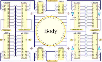
A high-spee As it is see used as the For a 3 are applied The multipl 32-electrode pin can be u
measureme
s stage the de digital valu nt part, AD1 itself, but its time (i.e. req to 260μs w tage signal
or sampling t is required ADC can sen
ed multiplex en in Fig. 12 analog multi 32-electrode for injection lexer is appli e system, 5 a used. Each la
ent
emodulated v ue is then tr 1674 with 12 s ADCs can quired time f which is not at a specifi time is exac d. This is du nse 2.44 mV
xer module w 2, the schem
iplexer in ou EIT system n and sink po ied for sharin address lines atch is applie
Fig. 12.
voltage is me ransmitted t 2-bit resolut nnot be used for conversio
an exact am ic point in ctly 10μs [22 e to the 12-changing on
5. MU
with 32 outp matic circuit o
ur design. m, eight ICs o
orts of curren ng the curren s are needed; ed for a pair o
. The proposed
easured, hen to the micro tion is applie d in measure on of an ana mount of tim the range o 2], hence it is bit resolutio n the analog
ULTIPLEX
puts can be a of the multip
of the menti nt source and nt source and ; hence four of ADG506A
d design for m
nce it must b ocontroller ( ed as an AD ement. Acco alog value to me. So it wou of micro sec s very interes on of the IC,
voltage (one
XER
added to the plexer modu
ioned multip d the others a d voltmeter b address line A (for lower
multiplexer mo
e converted (ATmega128 DC. ATmega ording to the valid digital uld not be p cond. Howe sting to captu , for amplitu e bit is used f
proposed in ule is illustra
plexer are req are used for between mul s of ADG50 and higher th
odule
from analog 8) of contro a128 has a n
e data-sheet l data) of its
ossible to ca ver, in AD ure the analo ude between for sign).
nstrumentatio ated. ADG50
quired. Four voltage mea ltiple electro 06AKN plus
han 16 electr
g to digital l unit. In number of [21], the ADCs, is apture the 1674, the og voltage
±5V, the
on design. 06AKN is
The con
Contro
Comm
Conne
Conne
Comm
As it c output ports the next stag
a) Data tran
Serial therefore co [23]. After register mu (ATmega12 voltage and COM port. microcontro rates such a
ntrol unit con olling the mu municating w
ecting to LCD ecting to AD municating w
can be seen s should be b
ges.
nsaction via
communicat onnecting the
completion ust be trans 28) is conne d vice versa.
. In this de oller frequen as 2.4, 9.6 an
ntains the fo ultiplexer pa with a PC and D (if require DC and contro with AVR pro
in Fig. 13, A buffered to a
Fig
RS-232
tion is one o e computer a of the volta smitted to cted to the . Hence the esign based ncy is assigne d 115.2 kbps
6. CO
llowing task art to determi d matching w ed), to display olling that as ogrammer fo
ATmega128 amplify the p
g. 13. The prop
of the proto and microco age measurem
the comput computer vi data transac on the stan ed on 14.745 s, the data tra
ONTROL UN
ks:
ine the state o with MATLA y the voltage s a slave with or programm
is applied a port output cu
posed design o
ocols that are ontroller, RS-ment, the m ter. In the ia MAX232, ction is done ndard freque 56MHz. In th ansaction err
NIT
of each elect AB for data tr
es and also n h handshakin
ing via ISP m
as the micro urrent and al
of control uni
e supported -232 commu measured volt proposed E , which conv e by RS-232 encies and he mentioned ror is zero.
trode on each ransaction vi
umber of me ng and interru mode.
ocontroller of lso to preven
t
by many ty unication pro tage stored i EIT system, verts the TT 2 serial com baud-rates d frequency
h moment. ia RS-232. easurements.
upting signa
f control uni nt the loading
ypes of com otocol is ofte in the micro , the micro TL voltage t mmunication (bps) table
for all stand .
ls.
it. All the g effect of
mputer and en applied ocontroller ocontroller o RS-232
baud-To show th stimulation cross pattern as the stimu
In the electrodes a applied thro procedure w pattern, it is the number pattern as th in the outer and decreas
Fig.
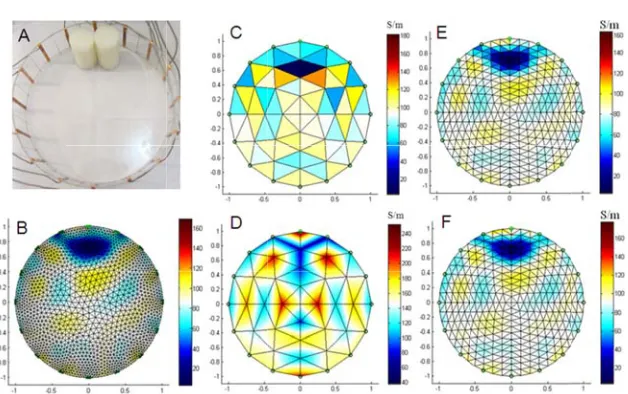
To evaluate cylindrical p will be show In all exper water. A cu electrodes. experiments cylindrical p
a) Experim
In the of a 16-elec image of su shown in F illustrated in parts C and
7
he experime (current inje n. In this pap ulation and m adjacent (ne and the volta ough the nex will be contin
s common to r of electrod
he system sti r region of th ses rapidly as
. 14. Adjacent
e performanc phantom wit wn and desc riments, the s urrent signal Adjacent p s. All imag phantom is m
ment 1
first experim ctrode cylind ubjects havi
ig. 15. Parts n parts C and
E the image
7. STIMULA
ental results ection) and per the adjac measurement eighboring) p ages are mea xt pair of elec
nued until ea o use all N × es. ATmega imulation an he imaged o s a function o
t pattern as the
ce of the sys th a few test cribed, and so
saline used i (~1mA) wit pattern is u ges are reco
made of Plex
ment two piec drical phanto ng less cond s B, E and F
d D. In parts e is reconstru
ATION AND
of the prop voltage mea cent pattern t topologies. pattern, show
sured from s ctrodes, and ach possible × (N − 3) me a128 in the c nd measurem
bject. The cu of distance.
e stimulation a
8. EXPERIM
stem to recon t objects. Th ome element in phantoms th 20 KHz fr sed as the onstructed b xiglas with a
ces of a plas om. The aim ductivity tha F show the fi s B, D, and F ucted onto ele
D MEASUR
posed EIT s asurement, su that is the mo
wn in Fig. 14 successive pa the voltage m pair of adjac easurements control unit ment protocol urrent densit and measurem MENTAL R nstruct imag he images rec
ts that can af is prepared w frequency is
stimulation by using the radius of 15c
stic (Teflon) m of experim an saline. Th fine-model im F the image o
ements.
REMENT PA
system, diffe uch as: adjac ost common
4, the curren airs of adjac measuremen cent electrod in most reco has been pr s. In this pat ty is highest
ment protocols
RESULTS
es, some exp constructed ffect the qua with solution injected to th and voltag e Eidors M
cm.
shaft have b ment is to eva he reconstru mages of pha of phantom, i
ATTERNS
erent topolog cent pattern,
pair-drive pr
nt is applied ent electrode nts will be rep des is used to
onstruction a rogrammed b ttern the curr t between the
s of the propos
periments w by using the ality of imag n of NaCl an he boundary ge measurem MATLAB pa
been placed i aluate the qu ucted images antom, and t is reconstruc
gies can be , opposite pa rotocol [24]
through two es. The curre peated for ot o inject curre algorithms, w based on the rent is injecte e injecting e
sed EIT system
were carried o e implemente ges will be in nd de-ionized y of phantom
ment protoc ackage [25,
in front of el uality of reco s of this pha the coarse m cted onto nod
used for attern and is applied
o adjacent ent is then thers. The ent. In this where N is e adjacent ed mainly electrodes,
m
out on the ed system ntroduced. d distilled ms via two col in all
26]. The
Fig. 15. (A) reconstructed elements. (F)
b) Experim
In this 4 and 14 of the quality Fig. 16 illus and coarse m
Fig. 16. (A) reconstructed elements. (F) c) Experim
In this cylindrical subjects in and coarse m
Phantom with d onto eleme ) Fine model r
ent 2
experiment, f a 16-electro
of reconstru strate the fin mesh genera
Phantom with d onto eleme ) Fine model r ment 3
experiment phantom. Th
different con models are sh
h two pieces ents. (D) Coa reconstructed
two pieces o ode cylindric ucted image o
nal reconstru ation models.
h two pieces o ents. (D) Coa reconstructed
, four pieces he experime
nductivities hown in part
of plastic sha arse model r onto nodes
of a metallic cal phantom of the subjec ucted images
of metallic sh arse model r onto nodes
s of the met nt is conduc
locating in ts B to F of F
aft. (B) Fine m econstructed
c (Aluminum with 30 cm cts having as
of the phan
haft. (B) Fine m econstructed
tallic and pla cted to evalu composite se Fig. 17.
model reconstr onto nodes.
m) shaft have diameter. Th s much cond ntom (shown
model reconst onto nodes.
astic shafts h uate the qual
etting. The f
ructed onto n (E) Fine mo
been placed he aim of thi ductivity as s in part A) b
tructed onto n (E) Fine mo
have been pu lity of recon final reconst
nodes. (C) Coa odel reconstru
d in front of e is test is to u saline. Parts by using diff
nodes. (C) Coa odel reconstru
ut in the 16-nstructed ima tructed imag
arse model ucted onto
electrodes understand B to F of ferent fine
arse model ucted onto
Fig. 17. (A) Coarse mod reconstructed d) Experim
In the phantom. T thorax-shap C (of Fig. 1
Fig. 18. (A) (C) Fine mod e) Experim
The aim images, and parameter. I hyper-param parameter s obtain a us causes the i action. As parameter v in terms of p
) Phantom wit del reconstruc
d onto elemen ment 4
following, th he goal of th pe phantom. A
8) the image
A 16-electrod del reconstruc ment 5
m of conduc d evaluate t In fact hype meter selecti selection sho seful recons image to be it can be se values are sh
precision and
th four pieces cted onto el nts. (F) Fine m
hree plastic a his test is eva As it can be e is reconstru
de thorax-shap cted onto node
cting this exp the quality r-parameter on is to prod ould produce
truction [24 dominated b een in Fig. hown. Obvio
d quality.
s of metallic a lements. (D) model reconstru
and metallic aluation of q seen in Fig. ucted onto no
pe phantom w es
periment is to of the fina (λ) is a scal duce the bes e solutions th 4]. Practicall
by noise and 19, few rec usly the reco
and plastic sha Coarse mod ucted onto no
subjects hav quality of the
18B, the im odes.
with some subj
o show the e l images re lar that contr st reconstruc hat preserve ly in image d as it is incr
onstructed im onstructed im
afts. (B) Fine del reconstru odes
ve been plac e images reco mage is recon
jects. (B) Fin
effects of hyp econstructed
rols the amo ction with hi as much of
reconstruct reased, noise mages of th mage with λ
model recons ucted onto n
ced in a 16-e onstructed by
structed onto
e model recon
per-paramete with differ unt of regul gh quality a f the measure
tion, insuffic is filtered th he phantom
= 0.01, repr
structed onto nodes. (E) Fi
electrode tho y using a 16-o elements, b
nstructed onto
er (λ) in reco ent values o arization. Th and resolutio
ed data as p cient hyper-p
hrough the s with differe resents the b
nodes. (C) ine model
orax-shape -electrode but in part
o elements.
onstructed of hyper-he goal of
n. Hyper-possible to
Fig. 19. Som EIT system. f) Experim
In the reconstructe frame acqui 16-electrode
In expe cylindrical p of voltage w noise can b reconstructe frames of v and F of Fig of voltage f of part C wh the average final recons
Fig. 20. Som four pieces o (D) n=5. (E)
me images whi The image wi ment 6
current ex ed image qu ired by scan e phantom ea eriment 6 so phantom as which means be seen on ed after scan voltages. So g. 20 are the frames. The
hich is recon e of voltage structed imag
me reconstruc of metallic an n=10. (F) 3D
ich were recon ith λ=0.01 rep
periment, ef ality will be nning an N-e ach frame of me metallic shown in Fig s that the ima this image nning ten tim the effects o 3D images o image in par nstructed afte frames inste ges would be
cted images of d plastic shaf image of pha
nstructed with presents the be
ffect of num e analyzed. In
lectrode pha f voltage con and plastic s g. 20.A. The age is recons (near electro mes, which m
of noise are i of the phanto rt F reconstr er scanning o ead of one fr e improved.
f one phantom fts. (B) n=1. ( antom in part A
h different λ v est image in te
mber of vo n fact, in adj antom is calc ntains 208 vo subjects are l e image in pa structed after odes 4, 8, 9 eans image r improved in om of part A ructed after s only one time frame, in ima
m, by using th (C) 3D image A with n=10
values (hyper-erms of precis
ltage frame djacent patter
culated by N oltages.
located in di art B is recon
r one time sc 9, and 10). H
reconstructio n the mention A, which are
scanning ten e. This result age reconstr
he average of (3D surface p
-parameter) by ion and qualit
or number rn the numbe N×(N – 3). H
ifferent posit nstructed by canning, ther However th on is done us ned image. T
reconstructe times is sm t can be extra ruction proce
fn voltage fra plot) of phant
y using the 16 ty
r of scannin er of voltage Hence after s
tions of a 16-using only o refore some e image in sing the aver The images i
d by differen oother than t acted so that ess, the qual
ames. (A) Pha tom in part A
6-electrode
ng in the es in each
canning a
-electrode one frame effects of part E is age of ten in parts C nt number the image t, by using lity of the
g) Experim
The ob image quali near the bou this test, th electrodes. evaluation i wall of the phantoms, i whereas in separated fr
Fig. 21. Rec electrodes to
The ne reconstructe applied as Adjacent pa central part electrodes, m
Fig. 22. Sho means of var
ment 7
bjective of ex ity. To evalu undary, in th hree phantom
The dimensi is near the b phantoms is in some plac reconstructe rom the boun
constructed im show their ac
ext position ed image of the stimulat attern, and i ts. It is sens
measuremen
owing quality rious numbers
xperiment 7 i uate the imag he central par ms are appl ions of phan boundary. As s about 2~3 ces show tha d images by ndary of phan
mages of subje ccuracy in fina
is the centr f subjects pu tion and me it is very se sitive to dis nt error and n
y of reconstru s of electrodes
is to show th ge quality, th rt and the wh lied with di ntoms and in
s it can be s cm, but in t at the dark p y 32-electrod
ntoms.
ects which are al image recon
ral part of t ut in the cen easurement t nsitive to co sturbances in noise as well
cted images o s
he effects of n hree position hole phantom
fferent num nternal saline
een in Fig. 2 the reconstru parts (smudg e phantom a
located near t nstruction qua
the phantom ntral part is topologies i onductive pa n the bound
[24, 27].
of the subject
number of el ns of a phant m (both centr mbers of elec e and subjec 21, the dista ucted images ges) are conn as it can be s
the boundary ality
m. As is illus poor. This i n all image arts near the dary shape o
t, which is loc
lectrodes in t tom surface ral part and n ctrodes whic cts are identi ance between s by 8-electr nected to th een, the dark
of phantoms w
strated in Fi is because th e reconstruct e boundary a of the object
cated in centr
the final reco would be co near the boun ch are 8, 1 ical. First po n subjects to rode and 16-e boundary k parts are co
with various n
ig. 22, the q he pattern w tions in this and insensiti t, the positio
ral part of pha
onstructed onsidered: ndary). In 6 and 32 osition for
the inner -electrode of image, ompletely
numbers of
quality of which was s paper is ive to the on of the
The la electrode ph the subjects the subjects shaft. But it of the 16-e instead of th
Fig. 23. Re different pos reconstructio
The re subjects loc instead of p Hence the adjacen parts near t decreased s phenomeno and 32-elec sensitivity. topologies, Although th resolution) extensively boundary vo regular med In this visually wit include an system desi electrode ph objects loca
As a m other, but th of Fig. 24 a
ast position i hantom is ve s which are lo s, there is a d t cannot be s
lectrode pha he central pla
econstructed i sitions of the on processes
econstructed cated near th plastic shaft! the result th nt pattern, wh
the boundary specifically on is that in ctrode phanto
Therefore the position
he EIT has b that still nee researched i oltage data a dical imaging s part, the qu th quality of
EIT system igned by Goh hantom and ated in phanto matter of fac
he size and p according to
is the whole ery crude, an ocated in the dark smudge seen in the re antom shows astic shaft it
images of thr phantom (cen
image of th e boundary,
hat can be ach hen the num y will be inc
when some 8-electrode p oms), and it
in image r of subjects i
9. VISU
been develop ed to be ove in clinical di and poor spat
g devices. uality of rec
images prod proposed b harian et al i from this po oms are mad t, the size of position of su their paper
e phantom. A nd it does not
e phantom. B e in the centr econstructed s the correct
shows a very
ree phantoms ntral part and
he 32-electro but it does n
heived from mber of elect
creased, but subjects ha phantom the causes more reconstructio is important a
UAL COMPA
ped substanti ercome to m iagnosis [29 tial resolutio
constructed i duced by usin
y Bera and in [32]. In fa oint of view t de from simil f all phantom ubjects in the
information
As shown in t have accep But despite th
ral part of th d image of 32
t position of y light smud
with differen near the boun
ode phantom not show any
this experim trodes of pha its sensitivi ave been loc e distance be e current den on accuracy as well, even
ARISON ON
ally over rec make it a clin , 30], but du on of image, t
image using ng other imp Nagaraju in act in both sy those system lar materials ms and test eir own phan
[31-32]. Th
n Fig. 23, th ptable accura
he bad qualit his image, as 2-electrode p f the subject dge.
nt numbers o ndary), and th
m also exact ything, even
ment is, for a antom increa ity to the cen cated near th etween electr nsity in the c y, related to
n when using
N RESOLU
cent years, th nically applic ue to poor Si
the EIT syste
g the propose plemented EI n [31] and a
ystems, imag ms are similar (plastic and objects are d ntoms are exa he mapped im
he reconstru acy to show t ty and showi the position phantom. Th
ts located ne
f electrodes. hese positions
tly shows th a light smud
n EIT system ases, the sys
ntral part of he boundary rodes is mor central part,
o measurem g 32-electrod
UTION
here are man cable imagin ignal to Nois ems have no
ed EIT syste IT systems. T DSP based ge is reconst r to the prop metal) as we different in c actly plotted mage of pha
ucted image the correct p ing inexact p n of the centr e reconstruc ear the boun
Subjects are s were identic
he correct po dge, in its ce
m that works stem sensitiv f the phantom y. The reaso
re than the o which result ment and st
de system.
ny challenges ng [28]. EIT
se Ratio (SN ot yet been ac
em will be The other EIT d multi-frequ
tructed by us posed system
ell.
comparison w in the middl antoms and t
of the 8-position of position of ral plastic ted image ndary, but located in cal in three
osition of entral part
s based on vity to the m will be on of this others (16 ts in more timulation
s (such as has been NR) of the ccepted as
compared T systems uency EIT
sing a 16-m. The test
objects (in m of real phan column sho objects. Th quality or re 32 electrod increased if
Fig. 24. Vis (A) reconstru using a DSP our EIT syste
In this pape detail. Syste shown. The Simplicity o EIT researc the practica output impe wasn’t poss system with
middle colum ntoms and the ows three 16 he third colu
esolution of r des of the im f the number
sual compariso ucted image b based multi-f em
er a practica em performa e novelty of of design ma chers for desi al point of vie edance of th sible to be m h 16 electro
mn of Fig. 24 eir container 6-electrode p umn shows t reconstructe mplemented of electrode
on on quality by using EIT frequency EIT
al low-cost p ance has been f this design
ade it possib igning and im ew to improv he current so measured w odes compar
4), have been rs applied in phantoms rel the reconstru
d image seen EIT system. s increases.
of final imag system propo T system propo
9. CO
precise desig n checked w n is its preci ble to have a
mplementati ve the precis ource, which with oscillosc
red to the o
n drawn with image recon lated to diff ucted image n in Fig. 24.C . Of course,
ges made by a osed by Bera osed by Goha
ONCLUSIO
gn of EIT in with a saline t
ision which a low-cost in on of EIT ha sion of the pr
h was finally cope. Higher
others is the
h the exact pr nstruction. As ferent EIT sy s made by t C is obtained the quality
applying three and Nagaraju arian et al in [3
ON
strumentatio tank and som
was achieve nstrumentatio ardware. Som roposed syste
y increased r quality of e best reaso
roportion com s it can be se ystems conta three differe d by using on and resolut
e different imp u in [31]. (B)
32]. (C) recon
on was propo me experime
ed without a on which co me hard wor em such as tr
to more tha the reconstr on to verify
mpared to di een in Fig. 24
aining saline ent EIT syst nly 16 electro tion of imag
plemented EI reconstructed nstructed imag
osed and des ental results h any complex ould pave the rk has been d rying to max an 5 MΩ su
ructed image the accurac
imensions 4, the first e and test tems. The odes from ge will be
T systems. d image by ge by using
scribed in have been x circuits. e way for done from ximize the uch that it
implemented EIT hardware. Future research includes improvement of the current EIT hardware in terms of accuracy and precision to become appropriate for clinical applications and development of EIT application in industrial and medical fields.
REFERENCES
1. Horesh, L. (2006). Some novel aproches in modelling and image reconstruction for multi-frequency electrical impedance tomography of the human brain. PhD thesis.
2. Denyer, C. W. L. (1996). Electronics for real-time and three-dimensional electrical impedance tomography. PhD thesis.
3. Yan, W., Hong, S. & Chaoshi, R. (2006). Optimum design of electrode structure and parameters in electrical impedance tomography. Physiol. Meas., Vol. 27, pp. 291-306.
4. Boone, K. G. & Holder, D. S. (1996). Current approaches to analogue instrumentation design in electrical impedance tomography. Physiol. Meas.17(suppl 1A) A229–A247.
5. Murphy, S. C., Chin, R. K. Y. & York, T. A. (2008). Design of an impeller-mounted electrode array for EIT imaging. Meas. Sci. Technol., Vol. 19, pp. 1-12.
6. Goharian, M., Soleimani, M., Jegatheesan, A., Chin, K. & Moran, G. R. (2008). A DSP based multi-frequency 3D electrical impedance tomography system. Ann. Biomed. Eng., Vol. 36, pp. 1594-1603.
7. Yorkey, T. J. (1986). Comparing reconstruction methods for electrical impedance tomography. PhD thesis, University of Wisconsin at Madison, Madison, WI 53706.
8. Filho, B., Brown, B. H. & Wilson, A. J. (2000). A comparison of modified Howland circuits as current generators with current mirror type circuits. Physiol.Meas., Vol. 21.
9. Holder, D. S. (2005). Electrical impedance tomography: methods, history and applications (Series in Medical Physics and Biomedical Engineering). Institute of Physics Publishing Ltd.
10. Khalighi, M., Vosoughi Vahdat, B., Mortazavi, M. & Soleimani, M. (2012). Practical design of low-cost instrumentation for industrial Electrical Impedance Tomography (EIT). IEEE I2MTC, Graz.
11. Zhao, D. (2011). High output-impedance current source for electrical impedance tomography. IEEE 4th International Conference on Biomedical Engineering and Informatics (BMEI).
12. Denyer, C., Lidgey, F. & Zhu, Q. (1994). A high output impedance current source. Physiol. Meas., Vol. 15, pp. A79-A82.
13. Kugelstadt, T. (2009). Active filter design techniques (chapter 20), Excerpted from OP AMPs for everyone. literature number: SLOD006A, published by Texas Instruments, third edition.
14. Cusick, G., Holder, D. S., Birkett, A. & Boone, K. (1994). A system for impedance imaging epilepsy in ambulatory human subjects. Innov. Tech. Biol. Med.15(suppl 1A) A33–A39.
15. Jossinet, J., Tourtel, G. & Jarry, R. (1994). Performance and operation of a set of wideband current generators for EIT. Innov. Tech. Biol. Med. 15(suppl 1A) A40–A46.
16. Zhang, Y. L., Zhui, X., Chaoshi, R., Wei, W., Dechun, Z. & Huiquan, Z. (2010). Study of voltage controlled current source in electrical impedance tomography system. IEEE, iCBBE, 4th Int. Conference.
17. Shuai, Z., Guizhi, X., Huanli, W. & Duyan, G. (2006). Multi-frequency EIT hardware system based on DSP. IEEE EMBS, 28th Annual international conference, China.
18. Smith, R. W. M. (1990). Design of a real-time impedance imaging system for medical applications”, PhD Thesis, University of Sheffield.
19. Soleimani, M. (1998). Designing and making the electrical impedance tomography systems. Sharif University of Technology, Msc thesis.
22. Data-she 23. Rahafroo 24. Graham,
lung ima 25. Vauhkon package 26. Adler, A Physiol. 27. Dickin,
Measure 28. Bayford
Biomedi 29. Brown, Science, 30. Hoetink blood vo Transac 31. Bera, T
inhomog 32. Goharian
3D elect 33. Khalighi current s
Fig. A1. (A) (C) VCCS b form 2 [9]
eet, (2000). AD oz, A. (2009). , B. M. (2007 aging. Univers nen, M., Lion
for the EIDO A. & Lionhea Meas.,Vol. 2 F. & Wang ement Science d, R. H. (200 ical Engineeri B. H. (2001). Measuremen , A. E., Faes, olume change
tion on Medic T. K. & Na geneities in 2D
n, M., Soleim trical impedan i, M., Vosou source for EIT
APPE A
VCCS based based on Trip
D1674, 12-bit . AVR Microc 7). Enhanceme
sity of Ottawa nheart, W. R. ORS project to art, W. R. B.
27.
, M. (1996). e and Technolo 06). Bioimped ing, Vol. 8, pp
Medical imp nt Science and T. J. C., Mar s during the h cal Imaging, V agaraju, J. (2 D-electrical im mani, M., Jega
nce tomograph ghi Vahdat, B T systems. IJR
NDIX A. SC AND THE RE
d on Advanced le-Operationa
t 100 kSPS A/D ontrollers and ents in Electri a. PhD thesis, B., Heikkinen o reconstruct tw
(2006). Uses
Electrical re ogy, Vol. 7, N dance tomogr p. 63-91. pedance tomog d Technology,
rcus, J. T., Ke heart cycle wit Vol. 21, Issue 2011). Resis mpedance tom atheesan, A., C
hy system. An B. & Mortaz RTET, Vol. 6,
CHEMATIC ESULTS OF
d Howland [1 al Amplifier f
/D converter. A d their applica ical Impedanc Degree in ele n, L. M., Vau wo dimension and abuses o
esistance tom No. 3, pp. 247-raphy (Electr
graphy and pr Vol. 12, No. 8 erkkamp, H. J.
th electrical im 6.
tivity imagin mography. Else Chin, K. & M nals of Biome zavi, M. (201 No. 2, DOI: 0
C CIRCUITS F PRIMARY
14, 15]. (B) V form 1 [17]. (
Analog Devic ations. Nas pu ce Tomograph ectrical and co
hkonen, P. J. nal EIT image of EIDORS:
mography for -260. rical impedan
rocess impeda 8, pp. 991–99 . J. & Heethaa mpedance usin
ng of a rec evier, Measure Moran, G. R. (
edical Enginee 1). Designing 01.IJRTET.06
S OF MENT Y PRACTIC
VCCS based on (D) VCCS ba
ces Inc., USA. ublishing. hy (EIT) imag omputing engi
& Kaipio, J. s. Physiol. Me an extensible
process app
nce tomograph
ance tomograp 6.
ar, R. M. (200 ng a linear spo
onfigurable p ement, Vol. 44 2008). A DSP ering, Vol. 36 g a practical
.02. 239.
TIONED VC CAL TESTS
n Double-Ope ased on Triple
ge reconstruct ineering.
P. (2001). A eas., Vol. 22. software bas
lications. IOP
hy). Annual
phy: a brief re
02). Imaging ot-electrode a
phantom wit 4, pp. 518-526 P based multi 6, No. 9.
high output
CCSS
erational Amp e-Operational
tion for 3D
MATLAB
se for EIT.
P Science,
Review of
eview. IOP
of thoracic array. IEEE
th circular 6.
-frequency
impedance
Figure A1 shows different schematic circuits of the VCCS which have been used in practical tests. As it can be seen in Table A1, the results of several experiments are shown briefly. These tests were done on the breadboard with different resistance values in condition of 20KHz frequency and 1mA load current. It can be concluded (from Table A1) that the VCCS based on TOA1 (fourth row) is the best choice to have an efficient voltage-controlled current source. It can support a load in range of 10Ω to 10KΩ linearly and also has more than 5MΩ output impedance which calculated with (4).
Table A1. The results of VCCS primary physical tests [33] VCCS
Type (KRΩ1) (KRΩ2) (KRΩ3) (KRΩ4) (KRΩ5 ) Allowable Load (Ω)
Measured (Ω)
PSPICE (Ω)
AH 1 2 1 1 1 10 ~ 1K 100K 420K
DOA 1 1 1 1 5 10 ~ 5K 3 M 5.3M
TOA1 1 1 1 1 5 10 ~ 10K >5 M 7.8M
TOA1 2 2 2 2 5 10 ~ 10K 1 M 3.9M
TOA1 5 5 5 5 5 10 ~ 10K 500K 1.6M
TOA1 10 10 10 10 5 10 ~ 10K 500K 770K
TOA1 22 22 22 22 5 10 ~ 10K 150K 340K
TOA1 27 27 27 27 5 10 ~ 10K 100K 280K
TOA2 1 1 1 1 5 10 ~ 10K 600K 2.5M