Adv. Radio Sci., 6, 219–225, 2008 www.adv-radio-sci.net/6/219/2008/
© Author(s) 2008. This work is distributed under the Creative Commons Attribution 3.0 License.
Advances in
Radio Science
Highly efficient integrated rectifier and voltage boosting circuits for
energy harvesting applications
D. Maurath, C. Peters, T. Hehn, M. Ortmanns, and Y. Manoli
Chair of Microelectronics, Department of Microsystems Engineering (IMTEK), University of Freiburg, Georges-Koehler-Allee 102, 79110 Freiburg, Germany
Abstract. This paper presents novel circuit concepts for
in-tegrated rectifiers and voltage converting interfaces for en-ergy harvesting micro-generators. In the context of en-ergy harvesting, usually only small voltages are supplied by vibration-driven generators. Therefore, rectification with minimum voltage losses and low reverse currents is an im-portant issue. This is realized by novel integrated rectifiers which were fabricated and are presented in this article. Ad-ditionally, there is a crucial need for dynamic load adapta-tion as well as voltage up-conversion. A circuit concept is presented, which is able to obtain both requirements. This generator interface adapts its input impedance for an opti-mal energy transfer efficiency. Furthermore, this generator interface provides implicit voltage up-conversion, whereas the generator output energy is stored on a buffer, which is connected to the output of the voltage converting interface. As simulations express, this fully integrated converter is able to boost ac-voltages greater than|0.35 V| to an output dc-voltage of 2.0 V–2.5 V. Thereby, high harvesting efficiencies above 80% are possible within the entire operational range.
1 Introduction
Especially electronic devices participate the development to-wards miniaturization and high performance with least power consumption only. Nowadays, very low power applications emerge increasingly in the field of stand-alone and wireless acting sensor/actuator-systems. A further rise of the applica-bility of such systems as fully embedded nodes suffers from the inconvenience with batteries. These electrochemical en-ergy storages have limited lifespan, are very temperature sen-sitive and need to be replaced repetitively. In case of hardly
Correspondence to: D. Maurath (maurath@imtek.de)
accessible locations, there is little chance for having battery power supply based cost-efficient wireless embedded sys-tems. Thus, the idea of power supplies, which are based on energy harvesting principles, is a helpful contribution in or-der to realize cost-efficient fully embedded sensor/actuator-systems.
A very space-efficient and robust kind of energy har-vesting is possible with vibration-driven inductive micro-generators. However, such micro-generators supply only small open-circuit output voltage in the range of 2–3 Vpp. Beside this, a relatively high internal resistive impedance causes only a small load optimum, were the maximum pos-sible output power is obtained. These circumstances enforce developments of novel kinds of rectifiers, since common full-wave rectifiers cause relatively high voltage losses.
In order to circumvent these crucial limitations, the second chapter shows enhanced rectifier circuitry with active diodes, which were designed, implemented and fabricated. These ac-tive diodes consist of an acac-tive circuit instead of passive de-vices only. Additionally, due to this low voltages and high in-ternal resistance an adaptive generator-interface is required. This interface gives the opportunity of most appropriate load-ing of the generator. Since only a simple capacitive energy buffer connected to the output of the rectifier can not provide adequate load matching. Due to the realization of this inter-face with switched-capacitors, the functionality of the rec-tifier is improved with respect to minimum input voltages. Conclusively, the forth chapter presents simulated as well as measured results. So, the active diodes of the proposed recti-fier without the generator interface can operate above 1.75 V generator output voltage amplitude. Together with the inter-face, generator output amplitudes of less than 1 V are suffi-cient for operation. Whereas the rectification, matching and conversion efficiencies can be kept above 80% over the entire operating range.
220 D. Maurath et al.: Highly efficient integrated rectifier and voltage boosting circuits for energy harvesting applications
energy harvesting with micro-generators this approach may
exhibit crucial drawbacks.
2.1
Conventional rectifier circuits
Conventional full-wave rectifiers suffer a relatively high and
unappreciated voltages loss of about
1
.
4
V
. In case of
Schot-tky diodes, that voltage loss could be reduced to around 0.6V,
however, those diodes have intrinsically higher reverse
cur-rent, which is also not acceptable. Concerning integrated
rectifiers, the diodes are realized with MOSFETs, because
pn junctions are often not specified in forward direction in
CMOS processes. The bulks of PMOS transistors must
al-ways be connected to the highest potential and of NMOS
to the lowest to avoid leakage currents and latch-up. A
dy-namic bulk regulation (Fig. 2b), consisting of two transistors,
avoids this and must be added to every transistor. Due to this,
the number of transistors and leakage increases.
Similarly, conventional full wave (F W) rectifiers use four
MOSFETs connected as diodes. Every half wave is used,
but the voltage drop is twice
V
tand strongly reduces the
available output voltage. A smart improvement is presented
in (Ghovanloo, 2004), which replaces two diode-connected
transistors with two cross-coupled transistors. Thus, only
one
V
tvoltage drop is lost.
2.2
Common conversion concepts
The common approach, as depicted in Fig. 1, is reasonable
in case of some energy storage elements, like a battery, as
a power source. However, if micro-generators are
consid-ered, power can be gathered only when the generator is
ex-ited. That means, in order to be able to supply an
applica-tion independent of the generator excitaapplica-tion, two concerns
are necessary. First, if the generator is excited most possible
Fig. 1.
Common single stage power conversion and generator
inter-facing approach
(
a
)
. The generator can only supply power within
conduction degree
α
(
b
)
.
Fig. 2.
Schematic of a negative voltage converter
(
a
)
, the bulk
reg-ulation configuration
(
b
)
, and the active diode principle
(
c
)
.
energy has to be harvested. Second, most of that maximum
possible energy need to be stored at some energy storage
ele-ment, like a buffer capacity. Additionally, in order to harvest
continuously the maximum possible energy, permanent
opti-mal generator loading for maximum generator output power
as well as efficient rectification, and voltage conversion are
required (Shengwen, 2005).
3
Proposed Harvesting Circuitry
The generator interface was especially designed to
incor-porate with inductive micro-generators (Spreemann, 2006;
Kulkarni, 2007). The internal source resistance of these
in-ductive generators is between
R
i= 1
−
5
k
Ω
. The generated
open-circuit output voltage has
2
.
8
V
ppat most and
frequen-cies are not higher then
f
gen= 500
Hz
.
3.1
Novel active rectifier
The main goals of this novel rectifier are the reduction of the
voltage drop over the MOSFETs and achievement of a high
efficiency. This rectifier can be separated into two stages: (i)
the negative voltage converter and (ii) the active diode part.
3.1.1
First stage: negative voltage converter (CON)
The first stage of the proposed rectifier circuit is used to
con-vert the negative half waves of the input sinusoidal wave into
positive ones. This conversion is done with only four
stan-dard CMOS transistors (see Fig. 2a). No special technology,
e.g. isolated transistors, is needed to realize this circuit. The
left side is realized with PMOS transistors and always
de-livers the highest potential at
V
into node A. The right side
consists of NMOS transistors and the low voltage potential is
at point B. No additional dynamic bulk regulation transistors
are necessary, because this is inherently given in this circuit.
Thus, the bulk of the PMOS transistors can be directly
con-nected to point A and the NMOS to point B. This reduces the
number of required transistors.
The ability to convert nearly the entire voltage applied at
the input to the output is the main advantage of this circuit.
Fig. 1. Common single stage power conversion and generator interfacing approach (a). The generator can only supply power within
conduction degreeα(b).
2 Dominic Maurath: Highly Efficient Integrated Rectifier and Voltage Boosting Circuits for Energy Harvesting Applications
2 Conventional harvesting interfaces
Common generator interfacing configurations are compara-ble to the configuration shown in Fig. 1a. Together with this simple structure also conventional circuit principles are usu-ally applied. In case of batteries as power sources, this ap-proach can be very useful and efficient. However, in case of energy harvesting with micro-generators this approach may exhibit crucial drawbacks.
2.1 Conventional rectifier circuits
Conventional full-wave rectifiers suffer a relatively high and unappreciated voltages loss of about1.4V. In case of Schot-tky diodes, that voltage loss could be reduced to around 0.6V, however, those diodes have intrinsically higher reverse cur-rent, which is also not acceptable. Concerning integrated rectifiers, the diodes are realized with MOSFETs, because pn junctions are often not specified in forward direction in CMOS processes. The bulks of PMOS transistors must al-ways be connected to the highest potential and of NMOS to the lowest to avoid leakage currents and latch-up. A dy-namic bulk regulation (Fig. 2b), consisting of two transistors, avoids this and must be added to every transistor. Due to this, the number of transistors and leakage increases.
Similarly, conventional full wave (F W) rectifiers use four MOSFETs connected as diodes. Every half wave is used, but the voltage drop is twice Vt and strongly reduces the
available output voltage. A smart improvement is presented in (Ghovanloo, 2004), which replaces two diode-connected transistors with two cross-coupled transistors. Thus, only oneVtvoltage drop is lost.
2.2 Common conversion concepts
The common approach, as depicted in Fig. 1, is reasonable in case of some energy storage elements, like a battery, as a power source. However, if micro-generators are consid-ered, power can be gathered only when the generator is ex-ited. That means, in order to be able to supply an applica-tion independent of the generator excitaapplica-tion, two concerns are necessary. First, if the generator is excited most possible
Fig. 1.Common single stage power conversion and generator inter-facing approach(a). The generator can only supply power within conduction degreeα(b).
Fig. 2.Schematic of a negative voltage converter(a), the bulk reg-ulation configuration(b), and the active diode principle(c).
energy has to be harvested. Second, most of that maximum possible energy need to be stored at some energy storage ele-ment, like a buffer capacity. Additionally, in order to harvest continuously the maximum possible energy, permanent opti-mal generator loading for maximum generator output power as well as efficient rectification, and voltage conversion are required (Shengwen, 2005).
3 Proposed Harvesting Circuitry
The generator interface was especially designed to incor-porate with inductive micro-generators (Spreemann, 2006; Kulkarni, 2007). The internal source resistance of these in-ductive generators is betweenRi= 1−5kΩ. The generated
open-circuit output voltage has2.8Vppat most and
frequen-cies are not higher thenfgen= 500Hz.
3.1 Novel active rectifier
The main goals of this novel rectifier are the reduction of the voltage drop over the MOSFETs and achievement of a high efficiency. This rectifier can be separated into two stages: (i) the negative voltage converter and (ii) the active diode part.
3.1.1 First stage: negative voltage converter (CON)
The first stage of the proposed rectifier circuit is used to con-vert the negative half waves of the input sinusoidal wave into positive ones. This conversion is done with only four stan-dard CMOS transistors (see Fig. 2a). No special technology, e.g. isolated transistors, is needed to realize this circuit. The left side is realized with PMOS transistors and always de-livers the highest potential atVin to node A. The right side
consists of NMOS transistors and the low voltage potential is at point B. No additional dynamic bulk regulation transistors are necessary, because this is inherently given in this circuit. Thus, the bulk of the PMOS transistors can be directly con-nected to point A and the NMOS to point B. This reduces the number of required transistors.
The ability to convert nearly the entire voltage applied at the input to the output is the main advantage of this circuit. Fig. 2. Schematic of a negative voltage converter (a), the bulk
reg-ulation configuration (b), and the active diode principle (c).
2 Conventional harvesting interfaces
Common generator interfacing configurations are compara-ble to the configuration shown in Fig. 1a. Together with this simple structure also conventional circuit principles are usu-ally applied. In case of batteries as power sources, this ap-proach can be very useful and efficient. However, in case of energy harvesting with micro-generators this approach may exhibit crucial drawbacks.
2.1 Conventional rectifier circuits
Conventional full-wave rectifiers suffer a relatively high and unappreciated voltages loss of about 1.4 V. In case of Schot-tky diodes, that voltage loss could be reduced to around 0.6 V, however, those diodes have intrinsically higher reverse cur-rent, which is also not acceptable. Concerning integrated rectifiers, the diodes are realized with MOSFETs, because pn junctions are often not specified in forward direction in CMOS processes. The bulks of PMOS transistors must al-ways be connected to the highest potential and of NMOS to the lowest to avoid leakage currents and latch-up. A dynamic bulk regulation (Fig. 2b), consisting of two transistors, avoids this and must be added to every transistor. Due to this, the number of transistors and leakage increases.
Dominic Maurath: Highly Efficient Integrated Rectifier and Voltage Boosting Circuits for Energy Harvesting Applications 3
Fig. 3.Schematic of the comparator circuit with differential stage, common-source output amplifier and inverter stage.
The voltage drop with this rectifier is less than10mV (Pe-ters, 2007) and the negative half wave is now converted into a positive one. But this circuit can not be used to charge a stor-age capacitor, because the current direction is not controlled and current back flow occurs. Due to this a second stage is necessary to realize a useful rectifier.
3.1.2 Second stage: active diode current barrier (AD)
The main function of the second rectifier stage is to control the current direction. This could be in the simplest case a conventional diode-connected MOSFET. Using this, a full wave rectifier with only one voltage dropVt over the tran-sistor results (CON D). This circuit is comparable to the full wave rectifier with switches (FW S), but it is less prone to latch-ups and uses only 7 compared to 12 transistors.
In order to achieve very high output voltages and high ef-ficiencies the diode should be replaced by another element, the active diode. This active diode works nearly as an ideal diode, with current flowing in only one direction and nearly no voltage drop. The main difference to an ideal diode is the current consumption of the device. A complex realization of an active diode is presented in (Lehmann, 2005). A control circuit is used to determine the conducting and non conduct-ing time of a MOSFET used as a switch. (Lam, 2005) needs two active diodes to realize a full wave rectifier. The active diode presented in this paper is simpler and based on a fast and low power comparator circuit (see Fig. 2c). MP is the switch which is controlled by the comparator. If the voltage at the anode is higher compared to the cathode the output of the comparator is0V and MP is on. If the cathode is higher the output is high and MP is off. The supply voltage of the comparator is taken from the storage capacitor. Using a PMOS transistor as switch no additional start-up circuit is necessary for this active diode.
The most important part of the active diode is the com-parator. A fast comparator with a low power consumption is needed. If the comparator is too slow not all available energy
Fig. 4.Building blocks of the two stage approach, which is includes an additional load-adaptive generator interface into the power con-version chain.
can be transferred to the capacitor and additionally current back flow occurs after the input voltage has passed the max-imum value. The implemented comparator (see Fig. 3) is simply based on a differential stage, a common-source output amplifier and an inverter. The inputvin,DC is connected to the cathode (C) (Fig. 2c) and is also the power supply of the comparator.vin,ACis connected to the alternating sinusoidal input wave (anode (A)). The overall current consumption is less than1µAfor an input voltage of±2.75V. The operation voltage range is between1.6V and3.75V. Combination of the negative voltage converter (CON) (Fig. 2a) with the ac-tive diode (Fig. 2c) overcomes the mentioned drawback.
3.2 Capacitive generator interface and converter
In order to harvest continuously the highest possible energy, the power electronic is again separated in two stages (see Fig. 4). The first stage is a generator interface and has to be optimized for adaptive impedance matching so as to load the generator as ideal as possible. In addition to that, this first stage also has to transfer the harvested energy most effi-ciently into a buffer. Thereby, the output voltage of the first stage is neither fixed nor regulated by the converter. For ef-ficient energy transfer, the output voltage is rather adapted to the buffer voltageVb(t). With appropriate dimensioning of the components, the buffer voltage will vary only little and slowly compared to the generator ac voltage. Thus, the sec-ond stage is realized as a dc/dc converter.
The here presented generator-interface works basically as a voltage converter with adaptive input impedance adap-tation, efficient energy transfer and implicit voltage up-conversion. By applying power saving circuit techniques, the power consumption of the control circuitry and switch driving should be less thenPtotal≤50µW.
3.2.1 Adaptive conversion principle
The proposed adaptive switching converter is based on two capacitor arrays, which toggle complementary-phased with frequencyfconvbetween a charging and a transfer state,Sc andStrespectively (see Fig. 5). Whereas, a conversion-cycle is the single succession ofScandSt. In the considered
con-Fig. 3. Schematic of the comparator circuit with differential stage,
common-source output amplifier and inverter stage.
Similarly, conventional full wave (F W) rectifiers use four MOSFETs connected as diodes. Every half wave is used, but the voltage drop is twice Vt and strongly reduces the available output voltage. A smart improvement is pre-sented in (Ghovanloo and Najafi, 2004), which replaces two diode-connected transistors with two cross-coupled transis-tors. Thus, only oneVtvoltage drop is lost.
2.2 Common conversion concepts
The common approach, as depicted in Fig. 1, is reasonable in case of some energy storage elements, like a battery, as a power source. However, if micro-generators are consid-ered, power can be gathered only when the generator is ex-ited. That means, in order to be able to supply an applica-tion independent of the generator excitaapplica-tion, two concerns are necessary. First, if the generator is excited most possible energy has to be harvested. Second, most of that maximum possible energy need to be stored at some energy storage ele-ment, like a buffer capacity. Additionally, in order to harvest continuously the maximum possible energy, permanent opti-mal generator loading for maximum generator output power as well as efficient rectification, and voltage conversion are required (Shengwen et al., 2005).
D. Maurath et al.: Highly efficient integrated rectifier and voltage boosting circuits for energy harvesting applications 221
Dominic Maurath: Highly Efficient Integrated Rectifier and Voltage Boosting Circuits for Energy Harvesting Applications 3
Fig. 3.
Schematic of the comparator circuit with differential stage,
common-source output amplifier and inverter stage.
The voltage drop with this rectifier is less than
10
mV
(Pe-ters, 2007) and the negative half wave is now converted into a
positive one. But this circuit can not be used to charge a
stor-age capacitor, because the current direction is not controlled
and current back flow occurs. Due to this a second stage is
necessary to realize a useful rectifier.
3.1.2
Second stage: active diode current barrier (AD)
The main function of the second rectifier stage is to control
the current direction. This could be in the simplest case a
conventional diode-connected MOSFET. Using this, a full
wave rectifier with only one voltage drop
V
tover the
tran-sistor results (CON D). This circuit is comparable to the full
wave rectifier with switches (FW S), but it is less prone to
latch-ups and uses only 7 compared to 12 transistors.
In order to achieve very high output voltages and high
ef-ficiencies the diode should be replaced by another element,
the active diode. This active diode works nearly as an ideal
diode, with current flowing in only one direction and nearly
no voltage drop. The main difference to an ideal diode is the
current consumption of the device. A complex realization of
an active diode is presented in (Lehmann, 2005). A control
circuit is used to determine the conducting and non
conduct-ing time of a MOSFET used as a switch. (Lam, 2005) needs
two active diodes to realize a full wave rectifier. The active
diode presented in this paper is simpler and based on a fast
and low power comparator circuit (see Fig. 2c). MP is the
switch which is controlled by the comparator. If the voltage
at the anode is higher compared to the cathode the output
of the comparator is
0
V
and MP is on. If the cathode is
higher the output is high and MP is off. The supply voltage
of the comparator is taken from the storage capacitor. Using
a PMOS transistor as switch no additional start-up circuit is
necessary for this active diode.
The most important part of the active diode is the
com-parator. A fast comparator with a low power consumption is
needed. If the comparator is too slow not all available energy
Fig. 4.
Building blocks of the two stage approach, which is includes
an additional load-adaptive generator interface into the power
con-version chain.
can be transferred to the capacitor and additionally current
back flow occurs after the input voltage has passed the
max-imum value. The implemented comparator (see Fig. 3) is
simply based on a differential stage, a common-source output
amplifier and an inverter. The input
v
in,DCis connected to
the cathode (C) (Fig. 2c) and is also the power supply of the
comparator.
v
in,ACis connected to the alternating sinusoidal
input wave (anode (A)). The overall current consumption is
less than
1
µA
for an input voltage of
±
2
.
75
V
. The operation
voltage range is between
1
.
6
V
and
3
.
75
V
. Combination of
the negative voltage converter (CON) (Fig. 2a) with the
ac-tive diode (Fig. 2c) overcomes the mentioned drawback.
3.2
Capacitive generator interface and converter
In order to harvest continuously the highest possible energy,
the power electronic is again separated in two stages (see
Fig. 4). The first stage is a generator interface and has to
be optimized for adaptive impedance matching so as to load
the generator as ideal as possible. In addition to that, this
first stage also has to transfer the harvested energy most
effi-ciently into a buffer. Thereby, the output voltage of the first
stage is neither fixed nor regulated by the converter. For
ef-ficient energy transfer, the output voltage is rather adapted to
the buffer voltage
V
b(
t
)
. With appropriate dimensioning of
the components, the buffer voltage will vary only little and
slowly compared to the generator ac voltage. Thus, the
sec-ond stage is realized as a dc/dc converter.
The here presented generator-interface works basically as
a voltage converter with adaptive input impedance
adap-tation, efficient energy transfer and implicit voltage
up-conversion. By applying power saving circuit techniques,
the power consumption of the control circuitry and switch
driving should be less then
P
total≤
50
µW
.
3.2.1
Adaptive conversion principle
The proposed adaptive switching converter is based on two
capacitor arrays, which toggle complementary-phased with
frequency
f
convbetween a charging and a transfer state,
S
cand
S
trespectively (see Fig. 5). Whereas, a conversion-cycle
is the single succession of
S
cand
S
t. In the considered
con-Fig. 4. Building blocks of the two stage approach, which is includes an additional load-adaptive generator interface into the power conversion
chain.
3 Proposed harvesting circuitry
The generator interface was especially designed to incor-porate with inductive micro-generators (Spreemann, 2006; Kulkarni et al., 2007). The internal source resistance of these inductive generators is betweenRi=1−5k. The generated open-circuit output voltage has 2.8Vppat most and frequen-cies are not higher thenfgen=500 Hz.
3.1 Novel active rectifier
The main goals of this novel rectifier are the reduction of the voltage drop over the MOSFETs and achievement of a high efficiency. This rectifier can be separated into two stages: (i) the negative voltage converter and (ii) the active diode part. 3.1.1 First stage: negative voltage converter (CON) The first stage of the proposed rectifier circuit is used to con-vert the negative half waves of the input sinusoidal wave into positive ones. This conversion is done with only four stan-dard CMOS transistors (see Fig. 2a). No special technology, e.g. isolated transistors, is needed to realize this circuit. The left side is realized with PMOS transistors and always de-livers the highest potential atVin to node A. The right side consists of NMOS transistors and the low voltage potential is at point B. No additional dynamic bulk regulation transistors are necessary, because this is inherently given in this circuit. Thus, the bulk of the PMOS transistors can be directly con-nected to point A and the NMOS to point B. This reduces the number of required transistors.
The ability to convert nearly the entire voltage applied at the input to the output is the main advantage of this circuit. The voltage drop with this rectifier is less than 10 mV (Pe-ters et al., 2007) and the negative half wave is now converted into a positive one. But this circuit can not be used to charge a storage capacitor, because the current direction is not con-trolled and current back flow occurs. Due to this a second stage is necessary to realize a useful rectifier.
3.1.2 Second stage: active diode current barrier (AD) The main function of the second rectifier stage is to control the current direction. This could be in the simplest case a conventional diode-connected MOSFET. Using this, a full wave rectifier with only one voltage dropVt over the tran-sistor results (CON D). This circuit is comparable to the full wave rectifier with switches (FW S), but it is less prone to latch-ups and uses only 7 compared to 12 transistors.
In order to achieve very high output voltages and high ef-ficiencies the diode should be replaced by another element, the active diode. This active diode works nearly as an ideal diode, with current flowing in only one direction and nearly no voltage drop. The main difference to an ideal diode is the current consumption of the device. A complex realization of an active diode is presented in Lehmann and Moghe (2005). A control circuit is used to determine the conducting and non conducting time of a MOSFET used as a switch. Lam et al. (2005) needs two active diodes to realize a full wave rectifier. The active diode presented in this paper is simpler and based on a fast and low power comparator circuit (see Fig. 2c). MP is the switch which is controlled by the comparator. If the voltage at the anode is higher compared to the cathode the output of the comparator is 0 V and MP is on. If the cathode is higher the output is high and MP is off. The supply voltage of the comparator is taken from the storage capacitor. Using a PMOS transistor as switch no additional start-up circuit is necessary for this active diode.
The most important part of the active diode is the com-parator. A fast comparator with a low power consumption is needed. If the comparator is too slow not all available energy can be transferred to the capacitor and additionally current back flow occurs after the input voltage has passed the max-imum value. The implemented comparator (see Fig. 3) is simply based on a differential stage, a common-source out-put amplifier and an inverter. The inout-putvin,DCis connected to
the cathode (C) (Fig. 2c) and is also the power supply of the comparator.vin,ACis connected to the alternating sinusoidal input wave (anode (A)). The overall current consumption is less than 1µA for an input voltage of±2.75 V. The operation
222 D. Maurath et al.: Highly efficient integrated rectifier and voltage boosting circuits for energy harvesting applications lel. At this state, the capacitors are charged until the capacitor
voltagesVarray reach a certain voltage limitVstop, as shown
in Fig. 7. Afterwards, the array transitions to transfer state St. Therefore, the array capacitors have to be re-configured
so as to obtain a stacked voltageVstack, which is higher than
the buffer voltage Vb of an external buffer. In order to
ob-tain the dynamic adaptation of the optimal conversion ratio ki, the converter works in an oversampling manner. Thus, if
fgenfconv. is given, the conversion ratio can be adapted
quite continuously within a generator voltage period1/fgen.
3.2.2 Adaptive impedance matching
High internal generator resistance Ri requires a particular
converter design since an exceeding current load would cause a dramatic voltage breakdown, which would cause reduced generator output power. Due to the low output currents of energy harvesting generators (50 −500µA) capacitive voltage conversion is preferred rather than inductive conver-sion. However, charging a capacitor allows generally only attopt ≈ ln(2)maximum power transfer from the
genera-tor into the capacigenera-tor (see Fig. 6). The generagenera-tor-interface matching situation at topt is equivalent to the impedance
matching situation where Pgen(Ri = Rload) = Pmax
is achieved. Therefore, for optimal operation the capaci-tors charging level should stay around a optimal voltage of
Fig. 5.Schematic and state diagram of a conversion cycle cycle.
age up to a certain voltage.
3.2.3 Voltage conversion and array configuration
Due to the fact, that charge transfer from one capacitor to another one causes intrinsic losses due to series resistances (Gobbi, 2006). But by minimizing the initial voltage gap be-tweenVstackandVbthe charge transfer losses are minimized.
Hence, the optimal conversion ratiokiis obtained by
ki =
Vb
Vch,opt+ ∆Vch
= Vb Vstop
(1)
The strategy for stacking is that a maximum quantityni →
kmax of capacitors is used, whereas within each stack-stage
ni/ kicapacitors are connected in parallel (see Fig. 5). Thus,
the maximum capacitance for a certain conversion ratio is used, which reduces the conversion frequencyfconv.
4 Results
Generally, by application of the proposed energy harvesting circuit concepts more energy can be extracted out of the same micro-generator. The power and voltage losses are reduced and the load matching condition is improved.
Fig. 6.This plot shows the transient power transfer while an empty capacitor is charged.
Fig. 5. Schematic and state diagram of a conversion cycle cycle.
4 Dominic Maurath: Highly Efficient Integrated Rectifier and Voltage Boosting Circuits for Energy Harvesting Applications
verter both arrays consist ofkmax = 6capacitors, whereas kmaxdirectly corresponds to the maximum required voltage conversion ratio. However, the number of array capacitors ni, which are applied within a single conversion-cycle, is dy-namically adapted according to the current required conver-sion ratioki = Vb/Vgen(t). Hence, while one array is in charging stateSc,niarray capacitors out of thekmax avail-able array capacitors are connected to the generator in paral-lel. At this state, the capacitors are charged until the capacitor voltagesVarrayreach a certain voltage limitVstop, as shown in Fig. 7. Afterwards, the array transitions to transfer state St. Therefore, the array capacitors have to be re-configured so as to obtain a stacked voltageVstack, which is higher than the buffer voltageVb of an external buffer. In order to ob-tain the dynamic adaptation of the optimal conversion ratio ki, the converter works in an oversampling manner. Thus, if fgenfconv. is given, the conversion ratio can be adapted quite continuously within a generator voltage period1/fgen.
3.2.2 Adaptive impedance matching
High internal generator resistance Ri requires a particular converter design since an exceeding current load would cause a dramatic voltage breakdown, which would cause reduced generator output power. Due to the low output currents of energy harvesting generators (50−500µA) capacitive voltage conversion is preferred rather than inductive conver-sion. However, charging a capacitor allows generally only attopt ≈ ln(2)maximum power transfer from the genera-tor into the capacigenera-tor (see Fig. 6). The generagenera-tor-interface matching situation at topt is equivalent to the impedance matching situation where Pgen(Ri = Rload) = Pmax is achieved. Therefore, for optimal operation the capaci-tors charging level should stay around a optimal voltage of
Fig. 5.Schematic and state diagram of a conversion cycle cycle.
Vch,opt ≈Vgen(t), which corresponds totopt. This means, withinScthe generator charges the capacitors up toVstop= Vch,opt+∆Vch. Then the capacitors are toggled toStand dis-charged onto an output bufferCbuntil the capacitor voltage reaches ,∆Vch and∆Vdisch. The consequence of keeping the caps only in a small charging range of0.5Vgen(t)±∆V requires an increased number of capacitors. Thus, twice as many capacitors are implemented to boost the generator volt-age up to a certain voltvolt-age.
3.2.3 Voltage conversion and array configuration
Due to the fact, that charge transfer from one capacitor to another one causes intrinsic losses due to series resistances (Gobbi, 2006). But by minimizing the initial voltage gap be-tweenVstackandVbthe charge transfer losses are minimized. Hence, the optimal conversion ratiokiis obtained by
ki=
Vb Vch,opt+ ∆Vch
= Vb
Vstop
(1)
The strategy for stacking is that a maximum quantityni→ kmaxof capacitors is used, whereas within each stack-stage ni/ kicapacitors are connected in parallel (see Fig. 5). Thus, the maximum capacitance for a certain conversion ratio is used, which reduces the conversion frequencyfconv.
4 Results
Generally, by application of the proposed energy harvesting circuit concepts more energy can be extracted out of the same micro-generator. The power and voltage losses are reduced and the load matching condition is improved.
Fig. 6.This plot shows the transient power transfer while an empty capacitor is charged.
Fig. 6. This plot shows the transient power transfer while an empty
capacitor is charged.
voltage range is between 1.6 V and 3.75 V. Combination of the negative voltage converter (CON) (Fig. 2a) with the ac-tive diode (Fig. 2c) overcomes the mentioned drawback. 3.2 Capacitive generator interface and converter
In order to harvest continuously the highest possible energy, the power electronic is again separated in two stages (see Fig. 4). The first stage is a generator interface and has to be optimized for adaptive impedance matching so as to load the generator as ideal as possible. In addition to that, this first stage also has to transfer the harvested energy most effi-ciently into a buffer. Thereby, the output voltage of the first stage is neither fixed nor regulated by the converter. For ef-ficient energy transfer, the output voltage is rather adapted to the buffer voltageVb(t ). With appropriate dimensioning of the components, the buffer voltage will vary only little and
itor and ohmic load. Fig. 9 shows the transient behavior of the discussed rectifiers. For these simulations the frequency is125kHz, a capacitance of500pF and a load of 20kΩ
are used. For useful applications a larger capacitance value should be used to reduce the voltage ripple. But this value is more suitable for showing the excellent performance of the proposed rectifiers.
4.1.1 Rectifier output voltage comparison
Fig. 9 shows the input and the output wave form of the dis-cussed rectifiers. In this case the open circuit input voltage was±2.75V. The negative voltage converter in combina-tion with a PMOS diode (CON D) has nearly the same volt-age characteristic as the FW S. Both rectifiers with the active diode (HW AD and CON AD) reach nearly the input volt-age. The minimum voltage of the CON AD rectifier is also very high, because every half wave is used and the capacitor is charged up twice at each period.
4.1.2 Enhanced rectification efficiency
Beside the attainable output voltage the efficiency is also of importance. The efficiency of the different rectifiers versus the input amplitude is shown in Fig. 10. The use of an active diode in a half wave rectifier shows a strong increase of the efficiency (HW vs. HW AD). The highest efficiencies could
Fig. 7. This graph shows one conversion cycle, whereasVarrayis
the highest voltage within the array.
the dimensions are75×40µm.
Fig. 9.Simulation results of the output signal of the compared rec-tifiers. The output voltage range of CON D is in average less than the output voltage range of CON AD.
be reached using the negative voltage converter in combina-tion with the active diode (CON AD). The efficiency in this example is always larger than75%.
4.2 Interface matching and conversion results
Within all simulations and calculations, the generator was in-cluded as a sine wave source with an ohmic serial resistance. Because energy harvesting applications are considered, there are two important efficiencies:
ηT x=
1 (t2−t1)
Rt2
t1 VbIchdt ˆ
Vgen
4Ri
(2)
ηhvst=ηT x×ηconv =ηT x Rt2
t1 VloadIloaddt
Rt2
t1 VgenIgendt
(3)
Where (2) defines the input efficiency ηT x, which com-pares the theoretical maximum generator power to the actual
Fig. 7. This graph shows one conversion cycle, whereasVarrayis
the highest voltage within the array.
slowly compared to the generator ac voltage. Thus, the sec-ond stage is realized as a dc/dc converter.
The here presented generator-interface works basically as a voltage converter with adaptive input impedance adap-tation, efficient energy transfer and implicit voltage up-conversion. By applying power saving circuit techniques, the power consumption of the control circuitry and switch driving should be less thenPtotal≤50µW.
3.2.1 Adaptive conversion principle
The proposed adaptive switching converter is based on two capacitor arrays, which toggle complementary-phased with frequencyfconv between a charging and a transfer state,Sc and St, respectively (see Fig. 5). Whereas, a conversion-cycle is the single succession ofScandSt. In the considered converter both arrays consist ofkmax=6 capacitors, whereas kmaxdirectly corresponds to the maximum required voltage
conversion ratio. However, the number of array capacitors
ni, which are applied within a single conversion-cycle, is dy-namically adapted according to the current required conver-sion ratioki=Vb/Vgen(t ). Hence, while one array is in
charg-ing stateSc,ni array capacitors out of thekmaxavailable
ar-ray capacitors are connected to the generator in parallel. At this state, the capacitors are charged until the capacitor volt-agesVarray reach a certain voltage limitVstop, as shown in
Fig. 7. Afterwards, the array transitions to transfer stateSt. Therefore, the array capacitors have to be re-configured so as to obtain a stacked voltage Vstack, which is higher than
the buffer voltageVb of an external buffer. In order to ob-tain the dynamic adaptation of the optimal conversion ratio
ki, the converter works in an oversampling manner. Thus, iffgenfconv. is given, the conversion ratio can be adapted
quite continuously within a generator voltage period 1/fgen.
3.2.2 Adaptive impedance matching
High internal generator resistance Ri requires a particular converter design since an exceeding current load would cause a dramatic voltage breakdown, which would cause reduced
D. Maurath et al.: Highly efficient integrated rectifier and voltage boosting circuits for energy harvesting applications 223
Dominic Maurath: Highly Efficient Integrated Rectifier and Voltage Boosting Circuits for Energy Harvesting Applications 5
4.1
Rectification efficiencies
The main aspects of rectifiers are the maximum output
volt-age which can be reached and the efficiency
η
rect, which is
simply the quotient of the output and the input energy over
one period. The maximum achievable output voltage is
espe-cially important for energy harvesting with inductive
micro-generators.
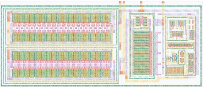
The circuits have been simulated and implemented with
Cadence using a
0
.
35
µm
HV CMOS C35 process from
aus-triamicrosystems (see Fig. 8). The voltage and efficiency
values strongly depend on the used frequency, storage
capac-itor and ohmic load. Fig. 9 shows the transient behavior of
the discussed rectifiers. For these simulations the frequency
is
125
kHz
, a capacitance of
500
pF
and a load of
20
k
Ω
are used. For useful applications a larger capacitance value
should be used to reduce the voltage ripple. But this value is
more suitable for showing the excellent performance of the
proposed rectifiers.
4.1.1
Rectifier output voltage comparison
Fig. 9 shows the input and the output wave form of the
dis-cussed rectifiers. In this case the open circuit input voltage
was
±
2
.
75
V
. The negative voltage converter in
combina-tion with a PMOS diode (CON D) has nearly the same
volt-age characteristic as the FW S. Both rectifiers with the active
diode (HW AD and CON AD) reach nearly the input
volt-age. The minimum voltage of the CON AD rectifier is also
very high, because every half wave is used and the capacitor
is charged up twice at each period.
4.1.2
Enhanced rectification efficiency
Beside the attainable output voltage the efficiency is also of
importance. The efficiency of the different rectifiers versus
the input amplitude is shown in Fig. 10. The use of an active
diode in a half wave rectifier shows a strong increase of the
efficiency (HW vs. HW AD). The highest efficiencies could
Fig. 7.
This graph shows one conversion cycle, whereas
V
arrayis
the highest voltage within the array.
Fig. 8.
The layout of the active diode enhanced rectifier, whereas
the dimensions are
75
×
40
µm
.
Fig. 9.
Simulation results of the output signal of the compared
rec-tifiers. The output voltage range of CON D is in average less than
the output voltage range of CON AD.
be reached using the negative voltage converter in
combina-tion with the active diode (CON AD). The efficiency in this
example is always larger than
75%.
4.2
Interface matching and conversion results
Within all simulations and calculations, the generator was
in-cluded as a sine wave source with an ohmic serial resistance.
Because energy harvesting applications are considered, there
are two important efficiencies:
η
T x=
1
(
t
2−
t
1)
R
t2t1
V
bI
chd
t
ˆVgen
4Ri
(2)
η
hvst=
η
T x×
η
conv=
η
T xR
t2t1
V
loadI
loadd
t
R
t2t1
V
genI
gend
t
(3)
Where (2) defines the input efficiency
η
T x, which
com-pares the theoretical maximum generator power to the actual
Fig. 8. The layout of the active diode enhanced rectifier, whereas the dimensions are 75×40µm.
generator output power. Due to the low output currents of energy harvesting generators (50−500µA) capacitive volt-age conversion is preferred rather than inductive conver-sion. However, charging a capacitor allows generally only at
topt≈ln(2)maximum power transfer from the generator into
the capacitor (see Fig. 6). The generator-interface matching situation attoptis equivalent to the impedance matching
situ-ation wherePgen(Ri=Rload)=Pmaxis achieved. Therefore,
for optimal operation the capacitors charging level should stay around a optimal voltage ofVch,opt≈Vgen(t ), which
cor-responds totopt. This means, withinScthe generator charges the capacitors up toVstop=Vch,opt+1Vch. Then the capaci-tors are toggled toStand discharged onto an output bufferCb until the capacitor voltage reaches ,1Vchand1Vdisch. The
consequence of keeping the caps only in a small charging range of 0.5Vgen(t )±1V requires an increased number of
capacitors. Thus, twice as many capacitors are implemented to boost the generator voltage up to a certain voltage.
3.2.3 Voltage conversion and array configuration
Due to the fact, that charge transfer from one capacitor to another one causes intrinsic losses due to series resistances (Gobbi et al., 2006). But by minimizing the initial voltage gap betweenVstackandVbthe charge transfer losses are min-imized. Hence, the optimal conversion ratioki is obtained by
ki =
Vb
Vch,opt+1Vch
= Vb
Vstop
(1)
The strategy for stacking is that a maximum quantity
ni→kmaxof capacitors is used, whereas within each
stack-stageni/ ki capacitors are connected in parallel (see Fig. 5). Thus, the maximum capacitance for a certain conversion ra-tio is used, which reduces the conversion frequencyfconv.
4 Results
Generally, by application of the proposed energy harvesting circuit concepts more energy can be extracted out of the same micro-generator. The power and voltage losses are reduced and the load matching condition is improved.
4.1 Rectification efficiencies
The main aspects of rectifiers are the maximum output volt-age which can be reached and the efficiencyηrect, which is
simply the quotient of the output and the input energy over one period. The maximum achievable output voltage is espe-cially important for energy harvesting with inductive micro-generators.
The circuits have been simulated and implemented with Cadence using a 0.35µm HV CMOS C35 process from aus-triamicrosystems (see Fig. 8). The voltage and efficiency values strongly depend on the used frequency, storage ca-pacitor and ohmic load. Figure 9 shows the transient behav-ior of the discussed rectifiers. For these simulations the fre-quency is 125 kHz, a capacitance of 500 pF and a load of 20 kare used. For useful applications a larger capacitance value should be used to reduce the voltage ripple. But this value is more suitable for showing the excellent performance of the proposed rectifiers.
4.1.1 Rectifier output voltage comparison
Figure 9 shows the input and the output wave form of the dis-cussed rectifiers. In this case the open circuit input voltage was±2.75 V. The negative voltage converter in combination with a PMOS diode (CON D) has nearly the same voltage characteristic as the FW S. Both rectifiers with the active diode (HW AD and CON AD) reach nearly the input volt-age. The minimum voltage of the CON AD rectifier is also very high, because every half wave is used and the capacitor is charged up twice at each period.
224 D. Maurath et al.: Highly efficient integrated rectifier and voltage boosting circuits for energy harvesting applications Dominic Maurath: Highly Efficient Integrated Rectifier and Voltage Boosting Circuits for Energy Harvesting Applications 5
4.1 Rectification efficiencies
The main aspects of rectifiers are the maximum output volt-age which can be reached and the efficiencyηrect, which is
simply the quotient of the output and the input energy over one period. The maximum achievable output voltage is espe-cially important for energy harvesting with inductive micro-generators.
The circuits have been simulated and implemented with Cadence using a0.35µmHV CMOS C35 process from aus-triamicrosystems (see Fig. 8). The voltage and efficiency values strongly depend on the used frequency, storage capac-itor and ohmic load. Fig. 9 shows the transient behavior of the discussed rectifiers. For these simulations the frequency is 125kHz, a capacitance of 500pF and a load of20kΩ are used. For useful applications a larger capacitance value should be used to reduce the voltage ripple. But this value is more suitable for showing the excellent performance of the proposed rectifiers.
4.1.1 Rectifier output voltage comparison
Fig. 9 shows the input and the output wave form of the dis-cussed rectifiers. In this case the open circuit input voltage was±2.75V. The negative voltage converter in combina-tion with a PMOS diode (CON D) has nearly the same volt-age characteristic as the FW S. Both rectifiers with the active diode (HW AD and CON AD) reach nearly the input volt-age. The minimum voltage of the CON AD rectifier is also very high, because every half wave is used and the capacitor is charged up twice at each period.
4.1.2 Enhanced rectification efficiency
Beside the attainable output voltage the efficiency is also of importance. The efficiency of the different rectifiers versus the input amplitude is shown in Fig. 10. The use of an active diode in a half wave rectifier shows a strong increase of the efficiency (HW vs. HW AD). The highest efficiencies could
Fig. 7. This graph shows one conversion cycle, whereasVarrayis the highest voltage within the array.
Fig. 8. The layout of the active diode enhanced rectifier, whereas the dimensions are75×40µm.
Fig. 9.Simulation results of the output signal of the compared rec-tifiers. The output voltage range of CON D is in average less than the output voltage range of CON AD.
be reached using the negative voltage converter in combina-tion with the active diode (CON AD). The efficiency in this example is always larger than75%.
4.2 Interface matching and conversion results
Within all simulations and calculations, the generator was in-cluded as a sine wave source with an ohmic serial resistance. Because energy harvesting applications are considered, there are two important efficiencies:
ηT x=
1 (t2−t1)
Rt2
t1 VbIchdt ˆ
Vgen
4Ri
(2)
ηhvst=ηT x×ηconv =ηT x
Rt2
t1 VloadIloaddt
Rt2
t1 VgenIgendt
(3)
Where (2) defines the input efficiency ηT x, which
com-pares the theoretical maximum generator power to the actual Fig. 9. Simulation results of the output signal of the compared
rec-tifiers. The output voltage range of CON D is in average less than the output voltage range of CON AD.
6 Dominic Maurath: Highly Efficient Integrated Rectifier and Voltage Boosting Circuits for Energy Harvesting Applications
Fig. 10. Efficiencies of the compared rectifiers plotted versus the input voltage.
converter input power. The higherηT xis, the better achieved
is impedance matching. In addition to this, the efficiency ηhvst in (3) gives a measure of the complete harvesting
ef-ficiency. This efficiency is mainly affected by internal con-verter losses and capacitor charge transfer losses. As Fig. 11a illustrates, the interface input power almost equals the maxi-mum possible output power.
Both graphs prove that this novel interface approach and conversion method operates as required. Generally, in order to characterize the efficiency by interfacing a generator, not onlyηconvcan be considered, but alsoηT xis of importance.
Therefore, Fig. 11b shows the overall harvesting efficiency ηhvstover the generator voltage range.
Fig. 11. The simulated efficiencies in graph (a) show the ratio of harvested power compared to maximum possible power, and (b) shows the overall conversion efficiency.
5 Conclusions
A novel rectifier concept consisting of a voltage converter and an active diode was presented. No additional bulk regu-lation transistors are needed and nearly the entire generator voltage appears at the rectifier output. In combination with a MOSFET diode the efficiency is about50%. In combina-tion with an active diode rectifier efficiencies over 90%can be reached. The maximum output voltage is only a few mV below the input voltage.
It was also shown, that high efficient power extraction and voltage up-conversion is feasible in energy harvesting envi-ronments. Especially the realization of adaptive impedance matching and almost continuous maximum generator power enhances the usage of micro-generators further. These ad-vantages give the opportunity of using smaller generators to supply autonomous applications. One drawback might be the relatively large quantity of capacitances, which need to be in-tegrated. Thus, a lot of chip area is necessary and parasitic effects could decrease the overall efficiency.
Acknowledgements. This work is supported by the German Re-search Foundation (Deutsche Forschungsgemeinschaft - DFG) un-der Grant Number GR1322 and MA 2193/7-1.
References
M. Ghovanloo, K. Najafi, ”Fully integrated wideband high-current rectifier for inductively powered devices”, IEEE Journal of Solid State Circuits, vol. 39, pp 1976-1984, 2004.
L. Gobbi, A. Cabrini, and G. Torelli, Impact of Parasitic Elements on CMOS Charge Pumps: a Numerical Analysis, IEEE Interna-tional Symposium on Circuits and Systems (ISCAS), May 2006. S. Kulkarni, E. Koukharenko, J. Tudor, S. Beeby, T. ODonnell, S. Roy, Fabrication and Test of Integrated Micro-Scale Vibration Based Electromagnetic Generator, International Solid-State Sen-sors Actuators and Microsystems Conference, 2007.
Y.-H. Lam, W.-H. Ki, C.-Y. Tsui, ”Integrated Low-Loss CMOS Ac-tive Rectifier for Wirelessly Powered Devices”, IEEE Trans. on Circuits and Systems, Vol. 53, No. 12, pp.1378-1382, 2006. T. Lehmann, Y. Moghe, ”On-chip active power rectifiers for
biomedical applications”, IEEE International Symposium on Circuits and Systems, Vol. 1, pp. 732-735, 2005.
C. Peters, O. Kessling, F. Henrici, M. Ortmanns, Y. Manoli, ”CMOS Integrated Highly Efficient Full Wave Rectifier”, IEEE IEEE In-ternational Symposium on Circuits and Systems (ISCAS), pp 2415-2418, New Orleans, 2007.
X. Shengwen, K.D.T. Ngo, T. Nishida, Ch. Gyo-Bum, A. Sharma, Converter and controller for micro-power energy harvesting, 20th Annual Applied Power Electronics Conference and Expo-sition, vol. 1, pp. 226- 230, March 2005.
D. Spreemann, B. Folkmer, D. Maurath and Y. Manoli, Tuneable transducer for low frequency vibrational energy harvesting, Eu-roSensors 2006, September 2006.
Fig. 10. Efficiencies of the compared rectifiers plotted versus the
input voltage.
4.1.2 Enhanced rectification efficiency
Beside the attainable output voltage the efficiency is also of importance. The efficiency of the different rectifiers versus the input amplitude is shown in Fig. 10. The use of an active diode in a half wave rectifier shows a strong increase of the efficiency (HW vs. HW AD). The highest efficiencies could be reached using the negative voltage converter in combina-tion with the active diode (CON AD). The efficiency in this example is always larger than 75%.
4.2 Interface matching and conversion results
Within all simulations and calculations, the generator was in-cluded as a sine wave source with an ohmic serial resistance. Because energy harvesting applications are considered, there
Fig. 10. Efficiencies of the compared rectifiers plotted versus the input voltage.
converter input power. The higherηT xis, the better achieved is impedance matching. In addition to this, the efficiency ηhvstin (3) gives a measure of the complete harvesting ef-ficiency. This efficiency is mainly affected by internal con-verter losses and capacitor charge transfer losses. As Fig. 11a illustrates, the interface input power almost equals the maxi-mum possible output power.
Both graphs prove that this novel interface approach and conversion method operates as required. Generally, in order to characterize the efficiency by interfacing a generator, not onlyηconvcan be considered, but alsoηT xis of importance. Therefore, Fig. 11b shows the overall harvesting efficiency ηhvstover the generator voltage range.
Fig. 11. The simulated efficiencies in graph (a) show the ratio of harvested power compared to maximum possible power, and (b) shows the overall conversion efficiency.
ronments. Especially the realization of adaptive impedance matching and almost continuous maximum generator power enhances the usage of micro-generators further. These ad-vantages give the opportunity of using smaller generators to supply autonomous applications. One drawback might be the relatively large quantity of capacitances, which need to be in-tegrated. Thus, a lot of chip area is necessary and parasitic effects could decrease the overall efficiency.
Acknowledgements. This work is supported by the German Re-search Foundation (Deutsche Forschungsgemeinschaft - DFG) un-der Grant Number GR1322 and MA 2193/7-1.
References
M. Ghovanloo, K. Najafi, ”Fully integrated wideband high-current rectifier for inductively powered devices”, IEEE Journal of Solid State Circuits, vol. 39, pp 1976-1984, 2004.
L. Gobbi, A. Cabrini, and G. Torelli, Impact of Parasitic Elements on CMOS Charge Pumps: a Numerical Analysis, IEEE Interna-tional Symposium on Circuits and Systems (ISCAS), May 2006. S. Kulkarni, E. Koukharenko, J. Tudor, S. Beeby, T. ODonnell, S. Roy, Fabrication and Test of Integrated Micro-Scale Vibration Based Electromagnetic Generator, International Solid-State Sen-sors Actuators and Microsystems Conference, 2007.
Y.-H. Lam, W.-H. Ki, C.-Y. Tsui, ”Integrated Low-Loss CMOS Ac-tive Rectifier for Wirelessly Powered Devices”, IEEE Trans. on Circuits and Systems, Vol. 53, No. 12, pp.1378-1382, 2006. T. Lehmann, Y. Moghe, ”On-chip active power rectifiers for
biomedical applications”, IEEE International Symposium on Circuits and Systems, Vol. 1, pp. 732-735, 2005.
C. Peters, O. Kessling, F. Henrici, M. Ortmanns, Y. Manoli, ”CMOS Integrated Highly Efficient Full Wave Rectifier”, IEEE IEEE In-ternational Symposium on Circuits and Systems (ISCAS), pp 2415-2418, New Orleans, 2007.
X. Shengwen, K.D.T. Ngo, T. Nishida, Ch. Gyo-Bum, A. Sharma, Converter and controller for micro-power energy harvesting, 20th Annual Applied Power Electronics Conference and Expo-sition, vol. 1, pp. 226- 230, March 2005.
D. Spreemann, B. Folkmer, D. Maurath and Y. Manoli, Tuneable transducer for low frequency vibrational energy harvesting, Eu-roSensors 2006, September 2006.
Fig. 11. The simulated efficiencies in graph (a) show the ratio of
harvested power compared to maximum possible power, and (b) shows the overall conversion efficiency.
are two important efficiencies:
ηT x= 1
(t2−t1)
Rt2
t1 VbIchdt
ˆ
Vgen
4Ri
(2)
ηhvst=ηT x×ηconv=ηT x Rt2
t1 VloadIloaddt Rt2
t1 VgenIgendt
(3)
Where Eq. (2) defines the input efficiencyηT x, which com-pares the theoretical maximum generator power to the actual converter input power. The higherηT xis, the better achieved is impedance matching. In addition to this, the efficiency
ηhvst in Eq. (3) gives a measure of the complete harvesting efficiency. This efficiency is mainly affected by internal con-verter losses and capacitor charge transfer losses. As Fig. 11a illustrates, the interface input power almost equals the maxi-mum possible output power.
Both graphs prove that this novel interface approach and conversion method operates as required. Generally, in order to characterize the efficiency by interfacing a generator, not onlyηconvcan be considered, but alsoηT x is of importance. Therefore, Fig. 11b shows the overall harvesting efficiency
ηhvstover the generator voltage range.
5 Conclusions
A novel rectifier concept consisting of a voltage converter and an active diode was presented. No additional bulk regu-lation transistors are needed and nearly the entire generator voltage appears at the rectifier output. In combination with a MOSFET diode the efficiency is about 50%. In combina-tion with an active diode rectifier efficiencies over 90% can
D. Maurath et al.: Highly efficient integrated rectifier and voltage boosting circuits for energy harvesting applications 225 be reached. The maximum output voltage is only a few mV
below the input voltage.
It was also shown, that high efficient power extraction and voltage up-conversion is feasible in energy harvesting envi-ronments. Especially the realization of adaptive impedance matching and almost continuous maximum generator power enhances the usage of micro-generators further. These ad-vantages give the opportunity of using smaller generators to supply autonomous applications. One drawback might be the relatively large quantity of capacitances, which need to be in-tegrated. Thus, a lot of chip area is necessary and parasitic effects could decrease the overall efficiency.
Acknowledgements. This work is supported by the German
Re-search Foundation (Deutsche Forschungsgemeinschaft – DFG) un-der Grant Number GR1322 and MA 2193/7-1.
References
Ghovanloo, M. and Najafi, K.: Fully integrated wideband high-current rectifier for inductively powered devices, IEEE J. Solid State Circuits, 39, 1976–1984, 2004.
Gobbi, L., Cabrini, A., and Torelli, G.: Impact of Parasitic Elements on CMOS Charge Pumps: a Numerical Analysis, IEEE Interna-tional Symposium on Circuits and Systems (ISCAS), May 2006.
Kulkarni, S., Koukharenko, E., Tudor, J., Beeby, S., O’Donnell, T., and Roy, S.: Fabrication and Test of Integrated Micro-Scale Vibration Based Electromagnetic Generator, International Solid-State Sensors Actuators and Microsystems Conference, 2007. Lam, Y.-H., Ki, W.-H., and Tsui, C.-Y.: Integrated Low-Loss
CMOS Active Rectifier for Wirelessly Powered Devices, IEEE Trans. Circuits and Systems, 53(12), 1378–1382, 2006. Lehmann, T. and Moghe, Y.: On-chip active power rectifiers for
biomedical applications, IEEE International Symposium on Cir-cuits and Systems, 1, 732–735, 2005.
Peters, C., Kessling, O., Henrici, F., Ortmanns, M., and Manoli, Y.: CMOS Integrated Highly Efficient Full Wave Rectifier, IEEE IEEE International Symposium on Circuits and Systems (IS-CAS), 2415–2418, New Orleans, 2007.
Shengwen, X., Ngo, K. D. T., Nishida, T., Gyo-Bum, Ch., and Sharma, A.: Converter and controller for micro-power energy harvesting, 20th Annual Applied Power Electronics Conference and Exposition, 1, 226–230, March 2005.
Spreemann, D., Folkmer, B., Maurath, D., and Manoli, Y.: Tune-able transducer for low frequency vibrational energy harvesting, EuroSensors 2006, September 2006.