method using measured transfer function
D. Rinas, J. Jia, A. Zeichner, and S. Frei
Dortmund University of Technology, Dortmund, Germany Correspondence to: D. Rinas ([email protected])
Abstract. Today EMC emissions of automotive components are often measured in anechoic chambers by an antenna at fixed position according to CISPR 25 (ALSE-method). The antenna voltage often cannot sufficiently describe the be-haviour of the measured electronic components and systems. Furthermore space requirements and costs are very high for the ALSE-method. Field- and cable-scan methods combined with near-field to far-field transformation techniques might be a good alternative.
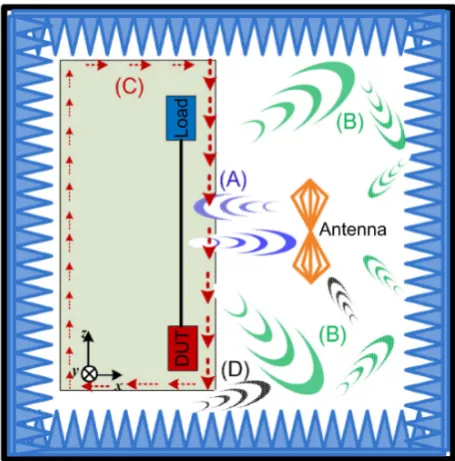
Residual reflections from the walls, the metallic floor, the measuring table, interaction of the antenna with the environ-ment, and other factors affect the measurements. Thus, mod-els which only regard the current distribution for near- and far field calculation cannot produce results equal to a cham-ber measurement.
In this paper methods for computing transfer functions for the substitution of EMC antenna measurements with field-and cable scans in a specified calibration area are introduced. To consider influences of the environment, the environment is characterized in a first step and included with transfer func-tions in the calculation process for the equivalent ALSE-field.
1 Introduction
Standardized component field measurement methods, like the ALSE antenna method defined e.g. in CISPR 25 (2007) for evaluation of electro-magnetic emissions from automo-tive systems, suffer from the need of large and expensive ane-choic chambers. Also a single field strength value is often not sufficient to characterize the EMI behavior of a complex sys-tem. Residual reflections from the walls, the metallic floor, the measuring table, interaction of the antenna with the en-vironment, and other influences affect the measurements and reduce reproducibility. Furthermore it is not possible to use
Fig. 1. Influencing factors of CISPR 25 ALSE method.
the measurement data for behavioral simulation model cre-ation. Alternative methods are necessary.
184 D. Rinas et al.: Substituting EMC emission measurement by field and cable scan method
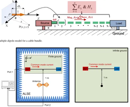
Fig. 2. Multiple-dipole-model for a cable bundle.
Fig. 3. CISPR 25 setup and simulation model. (a) Antenna measurement from cable bundle. (b) Field simulation from cable bundle by MoM.
Fig. 4. Transfer factor measurement setup.
respectively planar structure field scan methods are appli-cable (Rinas and Frei, 2012; Chen et al., 2009; Thomas et al., 2012). Here the current distribution on the PCB can be found through measuring the spatial magnetic field above the PCB. Including geometry properties and knowledge of pos-sible current paths the radiation model can be optimized.
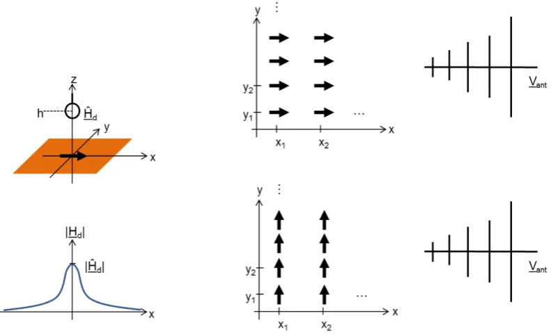
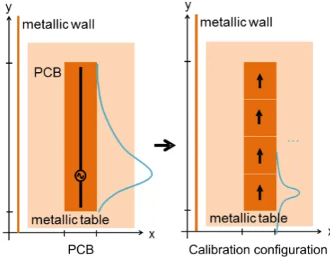
Fig. 5. Hertzian dipole configurations for calibration process. (a) Hertzian dipole and dipole near field. (b) Calibration inx- andy-direction for transfer function computation.
Fig. 6. Magnetic near field in each row and column of PCB can be
approximated by varying position of a set of dipoles.
2 Methods for substituting of antenna emission measurement
In the following sections the basic methods for antenna emis-sion measurement substitution are introduced. The differ-ences between cable bundle and PCB measurements are dis-cussed.
2.1 Cable bundles
In a radiation model a cable bundle can be divided into a set of short dipoles (Jia et al., 2012) as shown in Fig. 2. In this model, the influence of ground is incorporated into the radiation model using mirror theory which is actually differ-ent from real test configuration with more complex environ-ment, i.e. metallic table of limited size, large test antenna, non-perfect absorbing materials, and so on. Aiming at
inte-grating real influence factors in radiation models, we devel-oped two methods to correct calculated field result.
The proposed method calculates the absolute electric field at a reference point, the antenna center point. However, the test antenna converts the electric field around the antenna to a receiving voltage. In order to get the antenna field, the mea-sured voltage should be multiplied with the antenna factor (AF) provided by the antenna manufacturer. In real test con-figurations, the antenna is located in the near field from the cable bundle in a wide frequency range, while AF from man-ufacture is calibrated in far field in an open area test site. Therefore this antenna factor will not be accurate when used in near field test. We first measure antenna receiving volt-age radiated from cable bundle in standard configuration as shown in Fig. 3a and then use AF from manufacturer to ob-tain electric field at reference point (1 m distant to cable bun-dle). Subsequently we simulate the radiation from a verified MoM cable model to acquire electric field at the same point, as shown in Fig. 3b. Finally we can calculate the correction factor according to Eq. (1):
Emeasure=Vmeasure+AF(dB)
K=Emeasure−Esimulation(dB)
186 D. Rinas et al.: Substituting EMC emission measurement by field and cable scan method
Fig. 7. Process diagram of antenna emission measurement substitution.
Fig. 8. Setup for measurement of transfer functions and verification
of the method.
real test, we can directly evaluate the antenna voltage based on scanned currents of cable bundle (amplitude and phase) and transfer functionsTi.
S21=2×
V2
VS
=2×Ii×Zt VS
(2)
S31=2×
V3
VS
=2×Ui VS
(i=1· · ·N ) (3)
ILoad 11 ILoad 12 · · ·ILoad 1N ILoad 21 ILoad 22 · · ·ILoad 2N
..
. ... ... ... ILoad N1 ILoad N2 · · ·ILoad N3
T1 T2 .. . TN = U1 U2 .. . UN (4) 2.2 PCB
In Sect. 2.1 it is shown that the calibration between cable current and test antenna voltage can be computed by dividing a cable inNsegments and determining a transfer function for
Fig. 9. Electric field in vertical direction of measurement and
CASM.
each segment. In the same way a PCB can be discretised in N×M squares and transfer functions can be computed for each square inx- andy-current direction, as shown in Fig. 5b. As reference for calibration process and theoretical con-siderations a dipole antenna is applied. The magnetic near field in a plane above the dipole can be calculated or mea-sured (Rinas et al., 2011), as shown in Fig. 5a. The transfer function for each square is calculated by varying the position of the reference dipole along the squares, as shown in Fig. 5b.
Tnm,x= Vant
Hnm,x (5)
Tnm,y= Vant
Hnm,y (6)
where Tnm,x and Tnm,y are the transfer functions for the squares inx- and y-direction,Vantis the corresponding
an-tenna voltage and Hnm,xand Hnm,ythe measured magnetic fields.
Fig. 10. Antenna voltage from MoM and transfer function method. (a) Load: 1600. (b) Load: 400−500 µH−200 pF.
a dipoles can be found which best fits the magnetic field of each scanned row and column, as shown in Fig. 6. After that the transfer function for each dipole at new positions is in-terpolated. It should be noted that approximating the mag-netic field in amplitude and phase close to the source struc-ture is equal to approximating the current distribution. Know-ing current distribution voltage distribution is known to and magnetic and electric field can be calculated. Superposition of transfer function calibrated squares leads to calculation of resulting antenna voltage.
Vant=
X
TnmHnm (7)
The process diagram for PCBs is shown in Fig. 7.
3 Results
To show the applicability of the presented methods parts of results are based on Method of Moments (MoM) simulation data.
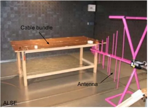
3.1 Cable bundles
In order to verify the proposed methods of correction factor and transfer function, we use an EMC antenna to test radi-ation from a simple cable, as shown in Fig. 8. The CASM method (Jia et al., 2012) was used to acquire amplitude and phase of currents along the cable and then electric field was calculated at the reference point using dipole model. We compared the results from measurement (measured antenna voltage plus antenna factor), CASM with mirror theory and CASM based on correction factor, as shown in Fig. 9. It can be seen that the resonances around 70 MHz and 350 MHz originating from test environment can be considered through correction factor. The deviation in high frequency is mainly
Fig. 11. Transfer function calibration of PCB with set of dipoles.
from measured current amplitude error and CASM algorithm itself.
188 D. Rinas et al.: Substituting EMC emission measurement by field and cable scan method
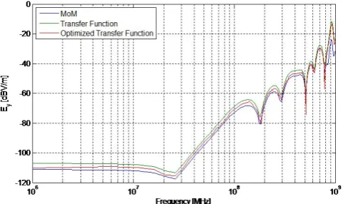
Fig. 12. Electric field calculated with transfer function and
opti-mized transfer function in comparison to electric field from MoM.
voltage measurements. But it is noted that the scanned cur-rent and voltage antenna here are based on simulation re-sults, which are free from noise, which can not be avoided in real measurements. The current and antenna voltage are both complex numbers in Eq. (4) which need amplitude and phase simultaneously.
3.2 PCB
For transfer function substitution, we present simulation re-sults by MoM method. The test PCB consists of a single ca-ble with a length of 0.16 m, a height over metallic plane of 5 mm, and two open ends. It is fed at length of 0.04 m with a supply voltage of 1 V. Transfer function calibration is done with four dipoles of finite length in a height of 5 mm above metallic plane, as shown in Fig. 11. According to Eqs. (5)– (7) transfer functionsTnmare computed and antenna voltage is calculated. To get better results approximation to near field distribution and transfer function interpolation is done.
Figure 12 presents the results of the substitution process. It can be seen that the electric field computed with transfer function shows good results up to a frequency of 800 MHz. Using near field approximation and transfer function inter-polation the results can be improved in the entire frequency range.
4 Conclusions
In this paper methods for substituting antenna emission mea-surements with field and cable scan methods are introduced. Influencing factors like interaction with antenna, wall reflec-tions, table currents and emission from measuring cable can be considered by use of measurement data from “calibration structures” and transfer functions. Cable bundles and PCBs are divided in segments and the transfer function can be com-puted for each of these segments. Superposition of the emis-sions gives the desired antenna voltage.
First results, partly based on MoM simulation data, are shown which proves the applicability of the proposed method. The investigations have to be extended in future.
Acknowledgements. The reported R + D work was carried out
within the CATRENE project CA310 EM4EM (Electromagnetic Reliability and Electronic Systems for Electro Mobility). This par-ticular research is supported by the BMBF (Bundesministerium fuer Bildung und Forschung) of the Federal Republic of Germany under grant 16 M3092 I. The responsibility for this publication is held by the authors only.
References
Chen, Q., Chakarothai, J., and Sawaya, K.: Estimation of Current Distribution by Near-Field Measurement, CEEM, China, 2009. CISPR 25 Ed. 3: Vehicles, boats and internal combustion engines –
Radio disturbance characteristics – Limits and methods of mea-surement for the protection of on-board receivers, IEC, 2007. Jia, J., Rinas, D., and Frei, S.: Prediction of Radiated Fields from
Cable Bundles based on Current Distribution Measurements, EMC Europe, Rome, 2012.
Smith, W. T. and Frazier, R. K.: Prediction of Anechoic Chamber Radiated Emissions Measurements Through Use of Empirically-Derived Transfer Functions and Laboratory Common-Mode Cur-rent Measurements, EMC, Denver, 1998.
Thomas, D. W. P., Obiekezie, C., Greedy, S., Nothofer, A., and Sewell, P.: Characterisation of Noisy Electromagnetic Fields from Circuits using the Correlation of Equivalent Sources, EMC Europe, Rome, 2012.
Rinas, D. and Frei, S.: Methoden zur Optimierung von St¨oraussendungsmodellen f¨ur Platinenstrukturen auf Basis von Nahfeldmessdaten, EMV D¨usseldorf, Germany, 2012.