Dynamic Analysis Model of a Class E
2Converter for Low Power Wireless Charging Links
Akram Bati
1, Patrick C.K. Luk
2, Samer Aldhaher
3, Chan H. See
1,4*,
Raed A. Abd-Alhameed
4,5, Peter S. Excell
61 School of Engineering, University of Bolton, Deane Road, Bolton, BL3 5AB, UK
2 Centre for Power Engineering, Cranfield University, College Road, Cranfield, MK43 0AL, UK
3 Department of Electrical and Electronic Engineering, Imperial College, Kensington, London, SW7 2AZ, UK 4 School of Electrical Engineering and Computer Science, University of Bradford, Bradford, BD7 1DP, UK
5Depart. of Communication and Informatics Eng., Basra University College of Science and Technology, Basra 61004, Iraq 6 Wrexham Glyndwr University, Wrexham, LL11 2AW, UK
Abstract:A dynamic response analysis model of a Class E2 converter for wireless power transfer applications is presented. The converter operates at 200 kHz and consists of an induction link with its primary coil driven by a class E inverter and the secondary coil with a voltage-driven class E synchronous rectifier. A 7th order linear time invariant state-space model is used to obtain the eigenvalues of the system for the four modes resulting from the operation of the converter switches. A participation factor for the four modes is used to find the actual operating point dominant poles for the system response. A dynamic analysis is carried out to investigate the effect of changing the separation distance between the two coils, based on converter performance and the changes required of some circuit parameters to achieve optimum efficiency and stability. The results show good performance in terms of efficiency (90-98%) and maintenance of constant output voltage with dynamic change of capacitance in the inverter. An experiment with coils of dimension of 53× 43× 6 mm3operating at a resonance frequency of 200 kHz, was created to verify the proposed mathematical model and both were found to be in excellent agreement.
1. Introduction
Wireless power transfer as a means of conveniently recharging consumer products is a growing trend. This is because the number of cordless devices has been rising rapidly and the changing of batteries or the plugging in of directly connected chargers is a burden which is irksome to busy lives: in addition, there is a significant risk of damage to contacts during plugging and unplugging operations. Wireless charging is inherently less efficient, but this is counterbalanced by its convenience and hence means are being sought to minimise energy losses and any other deleterious effects of energy leakage.
For the present work, the primary objective was the charging of batteries in electric drones, although other applications for the developed system can be envisaged. The order of magnitude of the desired transferred power was 20 W and the separation distance between charger and receiver was considered to be in the range from 1 to 15 mm.
The central power transfer component of a wireless charger is fundamentally an air-cored AC transformer. Air cores allow the fields to leak very substantially and hence, in terms of the equivalent circuit of a transformer [1,2], the mutual inductance is relatively low and the self-inductance of the windings is high. To minimise this effect, it is necessary to operate at a much higher frequency than standard power frequencies and also it is desirable to tune out the effect of the
self-inductance of the two windings by resonating them with capacitors.
There is an upper limit on the choice of frequency because power oscillators become inefficient above a few hundred kilohertz and rectifiers suffer similar problems. There is also a problem of leakage fields causing interference to radio communication systems, and this may force the use of unlicensed frequencies in the ISM (Industrial, Scientific and Medical) bands. However, the lowest ISM frequency is now 6.765 MHz [3], which is still a challengingly high frequency for efficient power transfer.
then required to maintain a constant output voltage produced from the WPT devices. To combat this problem, the authors in [15] suggested increasing the input voltage; however, this may lead to device breakdown and lower operating efficiencies due to the excessive heat generated. In [16-21] the, authors proposed the use of lossy, complex and bulky additional components and also power-consuming active devices for feedback and communications to achieve constant output voltage. Further, the authors in [22,23] suggested a nonradiative magnetic coupling approach to deliver power more efficiently; but the effective transfer range was basically restricted to one coil diameter unless relay resonators were adopted [24]. In [25,26] an optimized circuit structure was adopted which is based on series-shunt mixed resonant circuits but these circuits have poor efficiency, especially for long separation distances, despite the complexity of the circuits.
To clarify the differences between the presented work and other published works, Table I compares some technical details, i.e. Output power, Converter type and efficiency, for inductive power transfer (IPT).
Examining all the aforementioned methods, it is found that they either have poor efficiency or require high input power and complex structure to maintain a stable output voltage. In order to address these deficiencies, a dynamic analysis model was proposed to explore possibilities to solve this problem, taking into account that a control method is required in the transmitting circuit side that imposes no cost in power consumption and ensures constant output voltage and high efficiency operation. This model was implemented using a MATLAB SIMULINK environment. The aim of this work is to achieve constant and stable output voltage and the main objectives are:
• The examination of the Linear Time Invariant (LTI) state-space model corresponding to the switching operation of the converter switches.
• Maintaining constant and stable output voltage for variable separation distances.
• Improving the efficiency of the converter by changing the inverter capacitors.
The work included the effect of the variation of circuit parameters on the converter dominant Eigenvalues (poles) in the open loop condition. The complex s-plane was adopted in this analysis to identify the effective dominant pole that produce the circuit response under transient changes. For each switching period there is one dominant pole, which can be seen from its position on the complex plane, being the closest one to the imaginary axis. During one complete switching cycle with four transitions of ON-OFFing the MOSFET devices, the circuit will transit through four positions of dominant poles. The effective pole is calculated by using the participation factor and averaging through the four modes of switching positions in each cycle. Handling state-space models of such circuits in this manner makes the design of their controllers and regulators much easier. As a
result the circuit will be expected to obtain stable and constant output.
2. DESIGN AND METHODOLOGY
2.1. Mathematical Model
The basic circuit is shown in Fig. 1. This can be represented by the following differential equations derived for its equivalent circuit (shown in Fig. 2) based on Kirchhoff’s Voltage Law (KVL) and Kirchhoff’s Current Law (KCL):
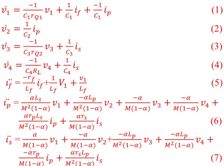
𝑣𝑣1̇ =𝐶𝐶1−1𝑟𝑟𝑄𝑄1𝑣𝑣1+𝐶𝐶11𝑖𝑖𝑓𝑓+−1𝐶𝐶1𝑖𝑖𝑝𝑝 (1)
𝑣𝑣2̇ =𝐶𝐶12𝑖𝑖𝑝𝑝 (2)
𝑣𝑣3̇ =𝐶𝐶3−1𝑟𝑟𝑄𝑄2𝑣𝑣3+𝐶𝐶13𝑖𝑖𝑠𝑠 (3)
𝑣𝑣4̇ =𝐶𝐶−14𝑅𝑅𝐿𝐿𝑣𝑣4+𝐶𝐶14𝑖𝑖𝑠𝑠 (4)
𝚤𝚤𝑓𝑓̈=−𝑟𝑟𝐿𝐿𝑓𝑓𝑓𝑓𝑖𝑖𝑓𝑓+𝐿𝐿1𝑓𝑓𝑉𝑉1+𝑣𝑣𝐿𝐿1𝑓𝑓 (5)
𝚤𝚤𝑝𝑝̈ =𝑀𝑀2𝛼𝛼𝐿𝐿(1−𝛼𝛼𝑠𝑠 )𝑣𝑣1+ −𝛼𝛼𝐿𝐿𝑝𝑝 𝑀𝑀2(1−𝛼𝛼)𝑣𝑣2+ −𝛼𝛼 𝑀𝑀(1−𝛼𝛼)𝑣𝑣3+ −𝛼𝛼 𝑀𝑀(1−𝛼𝛼)𝑣𝑣4+ 𝛼𝛼𝑟𝑟𝑝𝑝𝐿𝐿𝑠𝑠 𝑀𝑀2(1−𝛼𝛼)𝑖𝑖𝑝𝑝+𝑀𝑀(𝛼𝛼𝑟𝑟1−𝛼𝛼𝑠𝑠 )𝑖𝑖𝑠𝑠 (6)
𝚤𝚤𝑠𝑠̈ =𝑀𝑀(1−𝛼𝛼𝛼𝛼 )𝑣𝑣1+𝑀𝑀(−𝛼𝛼1−𝛼𝛼)𝑣𝑣2+𝑀𝑀−𝛼𝛼𝐿𝐿2(1−𝛼𝛼𝑝𝑝)𝑣𝑣3+ −𝛼𝛼𝐿𝐿𝑝𝑝 𝑀𝑀2(1−𝛼𝛼)𝑣𝑣4+ −𝛼𝛼𝑟𝑟𝑝𝑝 𝑀𝑀(1−𝛼𝛼)𝑖𝑖𝑝𝑝+ 𝛼𝛼𝑟𝑟𝑠𝑠𝐿𝐿𝑝𝑝 𝑀𝑀2(1−𝛼𝛼)𝑖𝑖𝑠𝑠 (7)
where 𝑣𝑣1,𝑣𝑣2,𝑣𝑣3 and𝑣𝑣4are the voltages across the capacitors C1,C2, C3 and C4 respectively. It should be noted that 𝑣𝑣4 is also the voltage across the load resistor RL and V1 is the input voltage. 𝑖𝑖𝑓𝑓 is the inductor current, 𝑖𝑖𝑝𝑝 and 𝑖𝑖𝑠𝑠 are the primary and secondary currents of the transformer respectively. 𝑟𝑟𝑝𝑝,𝐿𝐿𝑝𝑝, and 𝑟𝑟𝑠𝑠,𝐿𝐿𝑠𝑠 are the primary and secondary equivalent series resistances and inductances respectively, while M is the mutual inductance between them.
A zero equivalent series resistance is assumed for all capacitors. 𝐿𝐿𝑓𝑓 and 𝑟𝑟𝑓𝑓 are the DC-feed inductance and resistance of the inverter, 𝑅𝑅𝐿𝐿 is the load resistor and 𝛼𝛼=
𝐿𝐿𝑝𝑝𝐿𝐿𝑠𝑠− 𝑀𝑀2 .
Fig. 2 Equivalent circuit model of the Class E2 converter. In state-space form, equations 1 to 7 can be transformed into the following matrix form:
𝑥𝑥̇=𝐴𝐴.𝑥𝑥+𝐵𝐵.𝑈𝑈 (8) 𝑦𝑦=𝐶𝐶.𝑥𝑥+𝐷𝐷.𝑈𝑈
Where A is the state matrix, B is the input matrix, C is the output matrix (an identity matrix) and D is the feedforward matrix. 𝑥𝑥 represents the states (variables) vector.
𝑥𝑥= [𝑣𝑣1𝑣𝑣2𝑣𝑣3𝑣𝑣4𝑖𝑖𝑓𝑓𝑖𝑖𝑝𝑝𝑖𝑖𝑠𝑠 ]𝑇𝑇, A= [𝑎𝑎𝑖𝑖𝑖𝑖], B= [𝑏𝑏𝑖𝑖𝑖𝑖],𝑖𝑖=1,.. ,7 , and 𝑗𝑗=1,..,7
𝑈𝑈5=𝑉𝑉1 , D=0 , 𝑎𝑎11=𝐶𝐶1−1𝑟𝑟𝑄𝑄1 , 𝑎𝑎15 =𝐶𝐶11, 𝑎𝑎16=−1𝐶𝐶1
𝑎𝑎26=𝐶𝐶12, … … …𝑎𝑎77=𝑀𝑀𝛼𝛼𝑟𝑟2(𝑠𝑠1−𝛼𝛼𝐿𝐿𝑝𝑝) (9)
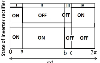
For dynamic analysis, it is assumed that switching ON and OFF of the two MOSFET devices connected across C1 and C3 can affect the values of coefficients 𝑎𝑎11and 𝑎𝑎33 only of the A-matrix. When the switch is in ON state, these coefficients have their normal values while when they are in their OFF states these two coefficients become zero. In this case, the system transits four states, representing the modes of switching in one cycle, as shown in Fig. 3. The corresponding circuit transfer function can be described by the following general form:
𝑌𝑌(𝑠𝑠)
𝑈𝑈(𝑠𝑠)=𝐶𝐶(𝑠𝑠𝑠𝑠 − 𝐴𝐴)−1𝐵𝐵 (10)
where s is the complex operator of the Laplace transform of the system differential equations and I is an identity matrix. Y(s) and U(s) are the Laplace Transforms of the output and input respectively.
The performance of the converter circuit can be determined in terms of the input function U and the initial state of the system 𝑥𝑥(0) or the initial conditions. The time domain solution can be described by the transition matrix
𝜑𝜑(𝑡𝑡) =𝐿𝐿−1{[𝑠𝑠𝑠𝑠 − 𝐴𝐴]−1}; the matrices B, C are constant matrices and D is a zero matrix. 𝜑𝜑(𝑡𝑡) also involves the inverse Laplace transform of a matrix inversion and the Eigenvalues are the solution of the characteristic equation |𝑠𝑠𝑠𝑠 − 𝐴𝐴|=0.
Fig. 3 The operating modes of the two MOSFETs for one switching cycle.
The four modes of the switching cycle were analyzed, based on the position of the dominant poles on the s-plane: these are the nearest poles to the imaginary axis of the s-plane.
Fig. 4 Step response of the converter linearized model.
A participation factor could be obtained as the ratio of each state time to the cycle period. Then at the end the effective dominant pole was determined by taking the average of the weighted dominant poles of the four states within the switching cycle. For the complex s-plane, the dominant pole can be described by the following complex number:
𝑠𝑠𝑑𝑑=𝜎𝜎±𝑗𝑗𝑗𝑗 (11)
𝑠𝑠𝑑𝑑 is the dominant pole; 𝜎𝜎 is the real part of the pole vector and should be negative for a stable system and 𝑗𝑗 is the imaginary part of the pole vector, also called the damped natural frequency of system response.
𝑗𝑗𝑛𝑛=√𝜎𝜎2+𝑗𝑗2 is the undamped natural frequency and
𝜁𝜁=𝜔𝜔𝜎𝜎
𝑛𝑛 is the damping ratio of the system.
The system is stable when its dominant pole has a negative real part. The system will have a better transient response if the dominant pole can be shifted to the left and closer to the real axis, i.e. larger 𝜎𝜎 and smaller ω, meaning higher damping and faster response. This is normally the task of the added controller.
If 𝑓𝑓1,𝑓𝑓2,𝑓𝑓3, and 𝑓𝑓4 are defined as the participation factors of the dominant poles, where
Where a is the time period of the first mode, (b-a) is the time period for the second mode, (c-b) is the time period for the third mode, and the time period for the fourth and last mode is (2𝜋𝜋 − 𝑐𝑐 ), as shown in Fig.3. The effective dominant pole (the average,
s
dav) can then be found by multiplying each dominant pole of Table 1 by its relevant participating factor and then divided by four which is the number of the operating modes in each switching cycle. The average dominant pole is:𝑠𝑠
𝑑𝑑𝑎𝑎𝑣𝑣=
𝑓𝑓1𝑠𝑠𝑑𝑑1+𝑓𝑓2𝑠𝑠𝑑𝑑2+𝑓𝑓4 3𝑠𝑠𝑑𝑑3+𝑓𝑓4𝑠𝑠𝑑𝑑4(12)
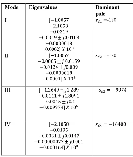
Table 1. The Eigenvalues and the dominant poles of the four modes of switching.
Mode Eigenvalues Dominant pole
I [−1.0057
−2.1058 −0.0219 −0.0019 ±𝑗𝑗0.0103
−0.0000018 -0.0002]𝑋𝑋 108
𝑠𝑠𝑑𝑑1=-180
II [−1.0057
−0.0005 ±𝑗𝑗 0.0159 −0.0124 ±𝑗𝑗0.009
−0.0000018 −0.0001]𝑋𝑋 108
𝑠𝑠𝑑𝑑2=-180
III [−1.2649 ±𝑗𝑗1.289 −0.0111 ±𝑗𝑗1.8091 −0.0015 ±𝑗𝑗0.1 −0.009974]𝑋𝑋 106
𝑠𝑠𝑑𝑑3=−9974
IV [−2.1058
−0.0195 −0.0031 ±𝑗𝑗0.0147 −0.00000077 ±𝑗𝑗0.001
−0.000164]𝑋𝑋 108
𝑠𝑠𝑑𝑑4=−16400
2.2. Eigenvalue Analysis and Equivalent Transfer Function
The Eigenvalues of the four switching modes shown in Fig. 3 with their dominant poles are presented in Table 1. These values were obtained from MATLAB based on calculation of the matrix A for each switching period.
The output to input voltage ratio of the converter transfer
functions TF for each mode of switching are given in eq. 13. The values in the numerators of eq. (13) are the gains of the
transfer functions. All these TFs do not have zeros but each has seven poles. In Table 1, the second column shows these poles and the dominant poles are shown in column three. The effective eigenvalue or the dominant pole is calculated by using the formula (12) as follows:
Where the calculated participation factors are 𝑓𝑓1=
0.14951, 𝑓𝑓2= 0.350488, 𝑓𝑓3= 0.13851, 𝑓𝑓4= 0.361489, and the calculated effective dominant pole, 𝑠𝑠𝑑𝑑𝑎𝑎𝑣𝑣=−1850. Now the effective transfer function can be expressed as eq. (14).
This can be reduced to:
TFav=(𝑠𝑠+18501850 ) (15) The dominant pole makes a journey, oscillating between the four modes (positions on the complex s-plane) during each switching cycle. This method of averaging the position of the dominant pole gives an accurate location for it, depending on the time period for each mode of operation.
The resultant position of the dominant pole s=-1850 is obtained from this averaging method. The other poles given in equation 15 are very far from the imaginary axis of the s-plane and have no effect on the converter response. The corresponding time response of this transfer function is plotted in Fig. 4.
2.3. Linearized SIMULINK Model
In order to capture converter dynamics, a linearized mathematical model is necessary to identify system response. It also helps in designing a controller that achieves constant output. Linearization of this model was carried out using built-in functions available from MATLAB SIMULINK software which are based on the output and input nodes that need to be identified. To effectively study this, an open loop class E2 converter model was established, for which the corresponding equation models can be found in Fig. 5.
3. Simulated Results and Discussion
3.1 Effect of Parameter Variation on System Dynamic Response
Looking at the effective dominant poles given in
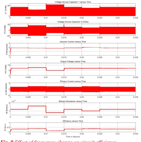
Equation 13, the circuit remains always stable with some amount of oscillations and this can be seen very clearly when separation distance between the primary and the secondary varies suddenly as this represents the most severe disturbance to the circuit. To better understand this, Fig. 6 depicts the time response variation of V1 (voltage across capacitor 1), V3 (voltage across capacitor 3), If (inductor current), V4 (output voltage) and Ip (transformer primary current) when the separation distance is changed from 1 mm to 8 mm, which is equivalent to changing M (mutual inductance) from 14 µH to 8 µH at time = 1 ms. As can be clearly seen, when the separation changes, the converter circuit goes through three stages of change, i.e. it builds up its magnetic flux, its transient response and then reaches a new steady state TFI= 1.04 𝑥𝑥 10
19
(𝑠𝑠+ 180)(𝑠𝑠+ 2.1 𝑥𝑥 104)(𝑠𝑠+ 2.2 𝑥𝑥 106)(𝑠𝑠+ 2 𝑥𝑥 104)(𝑠𝑠+ 1 𝑥𝑥 108)(𝑠𝑠2+ 3.86 𝑥𝑥 105𝑠𝑠+ 1.1 𝑥𝑥 1012)
TFII= 1.04 𝑥𝑥 10 19
(𝑠𝑠+ 180)(𝑠𝑠+ 1 𝑥𝑥 104)(𝑠𝑠+ 1 𝑥𝑥 106)(𝑠𝑠2+ 2.5 𝑥𝑥 106𝑠𝑠+ 2.3 𝑥𝑥 1012)(𝑠𝑠2+ 9.7 𝑥𝑥 104𝑠𝑠+ 2.5 𝑥𝑥 1012)
TFIII= 1.04 𝑥𝑥 10 19
(𝑠𝑠+ 9974)(𝑠𝑠2+ 3073𝑠𝑠+ 1 𝑥𝑥 109)(𝑠𝑠2+ 2.5 𝑥𝑥 106𝑠𝑠+ 3.6 𝑥𝑥 1012)(𝑠𝑠2+ 2.2 𝑥𝑥 104𝑠𝑠+ 3.27 𝑥𝑥 1012)
TFIV= 1.04 𝑥𝑥 10 19
(𝑠𝑠+ 2.1 𝑥𝑥 108)(𝑠𝑠+ 1.9𝑥𝑥 106)(𝑠𝑠+ 1.6 𝑥𝑥 104)(𝑠𝑠2+ 153.5𝑠𝑠+ 10 𝑥𝑥 1010)(𝑠𝑠2+ 6.1 𝑥𝑥 105𝑠𝑠+ 2.2 𝑥𝑥 1012)
(13)
TFav= 1.04 𝑥𝑥 10
19
(𝑠𝑠+ 1850)(𝑠𝑠+ 2.1𝑥𝑥 108)(𝑠𝑠+ 2.2 𝑥𝑥 106)(𝑠𝑠+ 1.64 𝑥𝑥 104)(𝑠𝑠2+ 3.86 𝑥𝑥 105𝑠𝑠+ 1.1 𝑥𝑥 1012)
(14)
condition. At the start, the separation distance is kept to its minimum, 1 mm, to see how the converter circuit builds its magnetic field for optimum mutual coupling between the two coils. It is clear from the responses that all variables (𝑥𝑥1…𝑥𝑥7) reach their steady state values in 0.54 ms. Then the transformer is disturbed suddenly by changing the separation distance to 8 mm. This represents the most severe potential disturbance to the converter.
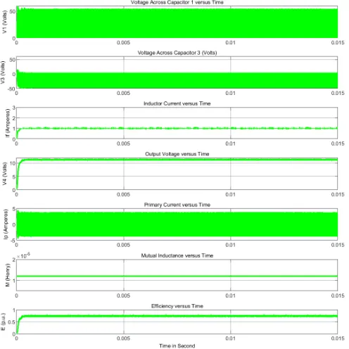
Fig. 7 describes the time response of V1, V3, V4, If, Ip, M and efficiency when the separation distance is changing repeatedly to different values. These responses show that the converter is sufficiently stable to cope with this type of cyclic disturbance. If the system is not sufficiently stable it will lose its stability with such types of cyclic disturbance. As can be observed, the converter cannot achieve both high output voltage and high efficiency: it needs adaptive parameters to be tuned to maintain its optimal working condition.
Fig. 6 Time response of the converter when separation distance
changes from 1 mm to 8 mm at T=1 ms. Fig. 7 Time response of the converter when separation distance changes to different values.
Fig. 8 Effect of changing C1 and C2 on efficiency, red curve-fixed
capacitors C1 and C2, green curve-tuned capacitors C1 and C2.
Fig. 9Effect of frequency change on circuit efficiency.
3.2. Improving Converter Efficiency 3.2.1. Changing Capacitors C1 and C2
Keeping the converter efficiency relatively high is a major challenge for such a circuit with a pre-determined resonance frequency. One of the suggested methods to improve its efficiency is by changing the frequency and/or the duty ratio of the two switching devices. However this entails the change of capacitor C3 to meet the desired operating resonant frequency as well as changing the values of capacitor C1 and C2 to maximize the efficiency.
Fig. 10 Results for the converter when f=217.243 kHz, RL=10 ohms,
D1=0.444, D2=0.501, delay angle of switch two=230.1°, k=0.55,
separation=3 mm.
Assuming that there is no control access to the receiver side (RS) of the converter, the only way to optimize the efficiency of the converter is at the transmitter side (TS). In this study, the values of capacitors C1 and C2 were changed simultaneously with the change in separation between the TS and the RS. Interestingly, it was found that, when C1 and C2 were increased to 70 nF and 64 nF respectively, higher efficiencies ranging from 90% to 98% were achieved with the change in the separation from 1 mm to 8 mm. This means that resonance is occurring and this leaves the circuit with its
inductor and winding resistances, which cause some power loss. This finding is in good agreement with [9]. To further comprehend this, Fig.8 depicts the efficiency achievement of the converter when C1 and C2 were allowed to change simultaneously with changes of separation.
3.2.2. Changing Frequency and Duty Ratio
In contrast to the achievement of good efficiency in the previous section, a change of frequency alone has a deleterious impact on circuit efficiency even if the capacitors’ values are changed accordingly. To verify this, the operating frequency of the proposed model was changed from 200 kHz to 160 kHz and the capacitors’ values were again optimized. As can be seen in Fig.9, poor efficiency is obtained, only generally around 24% on average. However, if the duty ratios of the two switches are changed simultaneously with the change of frequency, as well as altering the delay angle of switch 2 without changing the values of capacitors 1 and 2, the efficiency starts to improve, as shown in Fig. 10, assuming a fixed separation distance of 3 mm. This leads to a conclusion that changing frequency and duty ratios is another alternative to optimize the efficiency of the converter.
4. Experimental Setup and Verification
To verify the simulated results, an experiment was set up as shown in Fig.11 and the corresponding test bed parameters are tabulated in Table 2. The actual voltageacross MOSFETs Q1 and Q2 as well as the primary and secondary current responses obtained from the same converter used by [9] are verified by the simulation responses obtained from this work, as shown in figure 13. These responses also show that the optimum switching frequency is 200 kHz. The class E2 converter implemented in this work consisted of a Class E zero-voltage switching (ZVS) and zero-derivative voltage switching (ZDS) inverter with an infinite DC-feed inductance, an inductive link consisting of primary and secondary coils separated by a certain air gap and a voltage driven class E ZVS rectifier.
It is mentioned in [29] that efficient class E converter is attributed to its soft-switching capability.
The switch can undergo ZVS and ZDS only at optimum operating conditions. In this work the ZVS and ZDS conditions are satisfied because the chosen load resistance is changing between 5 and 10 Ohms: this is considered to be optimum for this type of converter. Thus the conditions stated in [29] are not violated.
Table 2. Measurement setup parameters for a variable load and variable coupling coefficient
6 14 0.5 212.6 0.426 0.471 233.4 27.89 35.27 3.24 2.17 0.95 4.61 10.12 7 10 0.45 187.7 0.543 0.519 228.8 34.49 52.79 6.9 3.7 2.6 8.77 13.72 8 10 0.47 192.1 0.526 0.516 229.2 33.37 49.11 6.18 3.5 2.27 7.98 12.87 9 10 0.52 206.1 0.48 0.507 230.1 30.53 40.17 4.63 2.99 1.55 6.24 10.72 10 10 0.55 217.2 0.444 0.501 229.8 28.68 34.59 3.77 2.63 1.16 2.48 8.72
The design procedure begins with coils of the inductive link: these coils should have a large quality (Q) factor at the switching frequency of the converter for maximum power transfer efficiency. Developing coils for inductive links is outside the scope of this paper as there is extensive research that has been devoted to this topic in literature. For this reason, the popular “Qi” Wireless Power Consortium standard [27] is adopted to determine the primary and secondary coils. Both coils have a maximum dc resistance of 0.1 Ω, an inductance of 24 μH, and a maximum Qfactor of
230 at 200 kHz [28]. The coils’ equivalent series resistance can be calculated and is equal to 0.137 Ω. With the addition
of the connectors’ resistance and the dc resistance of the printed circuit board tracks, the total resistance of the coils is approximately 0.18 Ω at 200 kHz.
The mutual inductance between the primary and secondary coils can be measured at different separation distances. For a separation distance of 3 mm, the measured mutual inductance is approximately 12 μH, which corresponds to a coupling coefficient (k) value of 0.50.
The secondary coil of the inductive link and capacitor C3 form the resonant part of the Class E rectifier. The value of C3that will cause the rectifier to resonate at 200 kHz is equal to 𝐶𝐶3=𝜔𝜔21𝐿𝐿𝑝𝑝= 26.38 𝑛𝑛𝑛𝑛 . The output capacitor C4 should be large enough to maintain a constant dc voltage. A value of
6.6 μF was found to be suitable. The capacitors used are
polypropylene capacitors from EPCOS [30]: according to their datasheet they have a dissipation factor of 0.002. Their ESR’s are assumed to be zero. The dimensions of the boards are equal to the coils, which are 53mm x 43mm, this is so that the inverter and rectifier boards could be placed behind the coils.
Fig. 11 Photograph of the Experimental Setup. Where the dimensions of the Tx and Rx coils are 53×43×6 mm3, and the
dimensions of their associated circuits are similar: 53×43×20 mm3
(approx.).
The inverter and rectifier switches are named Q1 and Q2 respectively. To drive MOSFET Q2 of the rectifier additional circuitry is needed to ensure that the switching signal is applied at the correct instants. Referring to the time instant c
in Fig. 3, MOSFET Q2 switches ON once the voltage across it crosses zero volts. Therefore, a comparator is used to trigger the switching signal using the voltage across this MOSFET. On the other hand, the voltage across MOSFET Q2 cannot be relied on as a trigger to turn it OFF. This is because the voltage has a near-zero time derivative. Therefore, a one-shot timer is used to drive MOSFET Q2 with a time duration equal to or less than duty cycle D2. The timer is triggered once the comparator detects a zero crossing in the voltage across MOSFET Q2.
The ZDS of the Class E inverter means that the first derivative of the voltage across switch Q1 is zero at the moment it is switched ON, which in turn results in zero- current switching. The switches are driven at the same switching frequency, but with different duty cycles.
separation distance between the two coils, selected capacitor values or switching frequencies are not the optimal values.
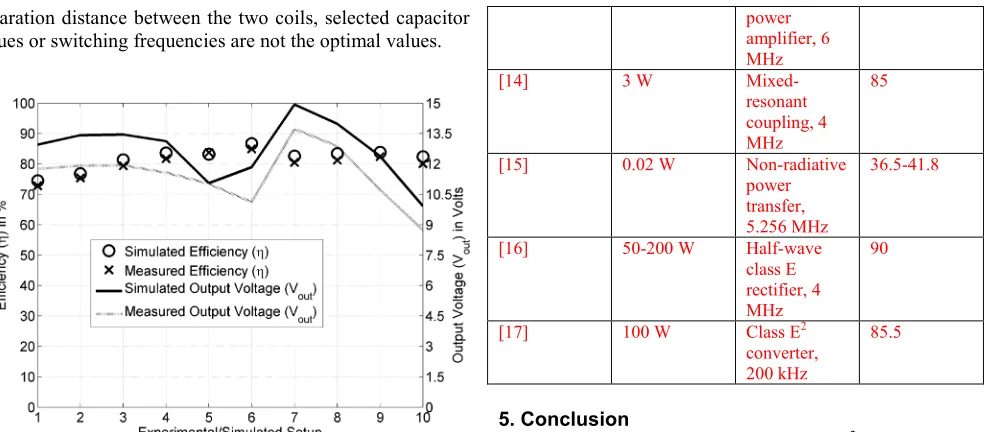
Fig.12 Simulated and Measured Efficiencies and Output Voltage
(Vout) of the Experiment Setups, with parameters as listed in Table 2
In Fig. 12 a comparison between the converter efficiency and output voltage for simulated results and those obtained from the experiment is shown, based on the configurations listed in Table 2. Fig.12 confirms that the simulated and measured results are in good agreement, particularly for the efficiency. There are small percentage errors that are attributable to the tolerance of the capacitors and other components used. It can be concluded that the circuit can achieve high levels of efficiency if the frequency, duty ratios and delay angles of the two switching devices can be altered dynamically.
Table 3 shows comparisons of the results of this work with other published work in terms of efficiency, taking into account the converter type used. This clearly shows the substantial advance that has been achieved in obtaining efficiencies that are close to the maximum possible for class E2 converters.
Table 3 CHARACTERISTICS OF PUBLISHED CLASS-E RECTIFIERS
Ref. Output Power Converter
Type 𝜂𝜂[%]
This work 20 W Class E2
converter, 200 kHz
90-98
[9] 20 W Class E2
converter, 200 kHz
92.32
[11] 10 W Class E
rectifier, Si Schottky
94
[12] 50 W Class E
power amplifier, 3.45 MHz
80
[13] 100 W Class E 77
power amplifier, 6 MHz
[14] 3 W
Mixed-resonant coupling, 4 MHz
85
[15] 0.02 W Non-radiative
power transfer, 5.256 MHz
36.5-41.8
[16] 50-200 W Half-wave
class E rectifier, 4 MHz
90
[17] 100 W Class E2
converter, 200 kHz
85.5
5. Conclusion
A dynamic analysis model of the E2 wireless power transfer converter has been presented. The results suggest the switching process of the MOSFET devices does not have a deleterious effect on the stability of the circuit but changing frequency or duty ratio causes the converter to operate at low efficiencies and this can cause instability. Remarkably, it is found that at a resonance frequency of 200 KHz, the dynamic change of transmitter side capacitors has achieved near-maximal efficiencies (90-98%) and maintained high output voltage. The high efficiency obtained is due to the resonance occurring in the converter by the action of the capacitors that compensate for some power loss in the inductor and windings resistances. The proposed work also suggests further development of optimally self-tuned regulators of such types for use in WPT devices. This can be done by changing the capacitors in the transmitter dynamically with the change in separation distances using a closed loop control system. The results confirmed that capacitor tuning produces almost stable output voltage and high efficiency. Experimental results verified the mathematical model, suggesting it is a reliable model for optimizing the performance of existing open loop WPT systems.
6. References
[1] A. Ayachit, M. Kazimierczuk, “Transfer functions of a transformer at different values of coupling coefficient”, IET Circuits, Devices & Systems Volume: 10 Issue: 4 Pages: 337-348, 2016.
[2] M. Kazimierczuk and Jacek Jozwik “Class E^2 narrow-band resonate dc/dc converter”, IEEE Trans. Instrumentation and Measurement, vol 38, no 6, pp. 1064-1068, Dec. 1989.
[3] OFCOM, Frequency bands designated for Industrial, Scientific and Medical use (ISM). UK Office of Communications, 2017. [4] Wireless Power Consortium. [Online] Available:
[5] M. M. K. Kazimierczuk and X. Bui, “Class E DC/DC converters with a capacitive impedance inverter,” IEEE Trans. Ind. Electron., vol. 36, no. 3, pp. 425–433, Aug. 1989.
[6] K.V. Schuylenbergh, and R. Puers, Inductive Powering: Basic Theory and Application to Biomedical Systems. New York: Springer-Verlag, Jul. 2009.
[7] Qualcomm Halo. [Online] Available: http://www.qualcommhalo.com/
[8] H. Wu, , G. Covic, J. Boys and D. Robertson, “A series-tuned inductive power-transfer pickup with a controllable AC-voltage output,” IEEE Trans. Power Electron., vol. 26, no. 1, pp. 98– 109, Jan. 2011.
[9] P.C.K. Luk, S. Aldhaher, W. Fei, and J. Whidborne, “State-Space Modelling of Class E2 Converter for Inductive Links”, IEEE Transaction on Power Electronics, vol.30, no. 6, pp.3242-3251, June 2015.
[10]S. Aldhaher, P.C.K. Luk and J. Whidborne, “Tuning Class E Inverters applied in Inductive Links Using Saturable Reactors”, IEEE Transaction on Power Electronics, vol.29, no.6, pp.2969-2978, June 2014.
[11]S. Aldhaher, P.C.K. Luk, K. Drissi, and J. Whidborne, “High-Input-Voltage High-Frequency Class E Rectifiers for Resonant Inductive Links”, IEEE Transaction on Power Electronics, vol.30, no.3, pp.1328-1335, March 2015.
[12]R.J. Calder, S.H. Lee, and R.D. Lorenz, “Efficient, MHz frequency resonant converter for sub-meter (30 cm) distance wireless power transfer”, in Proc. IEEE Energy Convers. Cong. Expo., pp.1917-1924, 2013
[13]M. Pinucla, D.C. Yates, S. Lucyszyn, and P.D. Mitcheson, “Maximizing DC-to-load efficiency for inductive power transfer”, IEEE Trans. Power Electronics, vol. 28, no. 5, pp. 2437-2447, May 2013.
[14]L. Chen, S. Liu, Y.C. Zhou, and T.J. Cui, “An optimizable circuit structure for high efficiency wireless power transfer”, IEEE Trans. Power Electronics, vol. 60, no. 1, pp. 339-349, Jan. 2013.
[15]E. M. Thomas, J. D. Heebl, C. Pfeiffer, and A. Grbic, “ A power link study wireless non-radiative power transfer system using resonant shielded loops”, IEEE Trans. Circuits systems I, vol. 59, no. 9, pp. 2125- 2136, Sept. 2012.
[16]S. Birca-Galateanu and J. L. Cocequerelle, “Class E half-wave low dv/dt rectifier operating in a range of frequencies around resonance”, IEEE Trans. Trans. Circuits systems I. vol. 42, no. 2, pp. 83-94, Feb. 1995.
[17]T. Nagashima, K. Inoue, X. Wei, E. Alarcon, and H. Sekiya, “Inductively coupled wireless power transfer with class e2 dc-dc converter”, in Circuit Theory and Design(ECCTD), 2013 European Conference on Sept. 2013, pp.1-4, 2013
[18]G. Wang, W. Liu, M. Sivaprakasam, and G. A. Kendir, “Design and analysis of an adaptive transcutaneous power telemetry for biomedical implants”, IEEE Trans. Circuits Syst. I, vol. 52, no. 10, pp. 2109-2117, Oct. 2005.
[19]Q. Chen, S. C. Wong, C. K. Tse, and X. Ruan,“ Analysis, design, and control of a Transcutaneous power regulator for artificial hearts”, IEEE Trans. Biomed. Circuits Syst. vol. 3, no. 1, pp. 23-31, Feb. 2009.
[20]P. Si., A. P. Hu, S. Malpas, and D. Budgett, “ A frequency control method for regulating Wireless power to implantable devices”, IEEE Trans. Biomed. Circuits Syst., vol. 2, no. 1, pp.22- 29, March 2008.
[21]A. Moradewicz and M. Kazmierkowski, “ Contactless energy transfer system with FPGA-controlled resonant converter”,
IEEE Trans. Ind. Electron., vol. 57, no. 9, pp. 3181-3190, Sept. 2010.
[22]Z.N. Low, R. A. Chinga, R. Tseng, and J. Lin, “Design and test of a high-power high-efficiency loosely coupled planar wireless power transfer system,” IEEE Trans. Ind. Electron., vol. 56, no. 5, pp. 1801– 1812, May 2009.
[23] J. J. Casanova, Z. N. Low, and J. Lin, “ A loosely coupled planar wireless power system for multiple receivers,” IEEE Trans. Ind. Electron., vol. 56, no. 8, pp. 3060– 3068, Aug. 2009.
[24]Y.- H. Kim, S.- Y. Kang, M.- L. Lee, B.- G. Yu, and T. Zyung, “Optimization of wireless power transmission through resonant coupling,” In Proc. CPE, 2009, pp. 426– 431, 2009
[25]R. P. Severns, “Topologies for three- element resonant converters,” IEEE Trans. Power Electron., vol. 7, no. 1, pp. 89– 98, Jan. 1992.
[26] L. Chen, S. Liu, Y.C. Zhou, and T.J. Cui, “An Optimizable Circuit Structure for High-Efficiency Wireless Power Transfer”, IEEE Trans. Ind. Electron., vol.60, No.1, pp 339-349, Jan. 2013.
[27]Wireless Power Consortium (Jun. 2013). [Online]. Available: http://www.wirelesspowerconsortium.com (accessed Jul. 2014).
[28]WE-WPCC Wireless Power Charging Coil
760308110.Datasheet, Wurth Elektronik, Niedernhall, Germany, 2013.
[29]A. Ayachit, F. Corti, A. Reatti and M. Kazimierczuk, “Zero-Voltage Switching Operation of Transformer Class-E Inverter at Any Coupling Coefficient”, IEEE Transactions on Industrial Electronics, May 2018. Early access: DOI: 10.1109/TIE.2018.2838059.