190 | P a g e
A STUDY OF SOI CMOS AND GAN MMIC
TECHNOLOGY FOR DEVELOPMENT OF LOW
POWER RF TRANSCEIVER
Sanjay S.Khonde
1, Dr.Ashok Ghatol
2, Dr.S.V.Dudul
3 1Research Scholar, Sant Gadge baba Amravati University, Amravati
2Former Vice Chancellor of BATU Lonere
3.Professor and Head, Department of Electronics, Sant Gadge Baba Amravati University, Amravati.
ABSTRACT
The recent trends shows that there are many upcoming semiconductor technologies used for developing low power RF transceiver required for wireless sensor node. The SOI CMOS and GaN MMIC technologies are most common out of them. The paper is divided into two parts. The first part of this paper consists of study of these two technologies based upon certain parameters like capability, device structure, device characteristics, effect of temperature, process of manufacturing the device etc. The second part discusses the device performance as an RF (Radio Frequency) circuit component necessary for high frequencies
Keywords: SOI CMOS, GaN MMIC, RF transceiver, low power
I. INTRODUCTION
The evolution of new semiconductor technology has improved performance of devices giving rise to more
power density, gain, noise figure, shrink in size and reduce power consumption. SOI CMOS is emerging process
from CMOS as compared to CMOS and BiCMOS with lots of advantages when high resistivity silicon substrate
is used.[7]The advantages which draw more attention are low loss, less noise and low leakage etc. The GaN
(Gallium Nitride technology), is revolutionary giving five times improvement in power density over the
traditional GaAs (Gallium Arsenide).Due to this it is now been used in MMIC ( Monolithic Microwave
Integrated Circuit) for next generation mobile Communication system and wireless sensor network.[11] The rest
of the paper contains background of these technologies and also the study based upon different parameters like
capability, device structure, device characteristics, effect of temperature, process and applications.
II. BACKGROUND
GaN semiconductors were studied 30 years ago and due to their wide bandgap, high breakdown field and high
saturated electron mobility velocity were considered ideal in comparison with other semiconductors.CMOS
technology was invented in 1963 by Frank wanlass Fairchild semiconductor.[1]SOI CMOS technology is one of
the best for high temperature applications due to low leakage current, temperature resistant threshold voltage,
191 | P a g e
III. GaN/SOI COMPARED AND CONSTRASTED
This section compares and contrast individual aspects of the two technologies based upon the following points
1) Capability: The device can be manufactured equally effectively in both SOI CMOS and GaN technology. The major application is next generation radar, communication system and RF System- on- Chip. The mimic’s
are usually used for designing very high frequency and high powered electronics circuits. The major beneficial
areas are cost, reliability, reproducibility, low size. In both the techniques all passive and active circuit elements
and interconnections are formed into a bulk or on to a substrate with some deposition process. SOI CMOS
technologies are very attractive options for implementing high speed digital integrated circuits for low power
application.
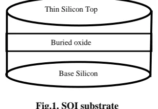
2) Device Structure: SOI means silicon on insulator structure in which the devices on silicon thin film exists on insulator film. SOI CMOS devices are separated into Si supporting substrate and buried oxide film (BOX).[4]
These device are structured so each element is completely isolated by local oxidation of silicon oxide film and
operating area is isolated by insulators. The SOI layer may be as thin as less than 50 nm and as thick as greater
than 100 nm. The buried oxide film reduces the junction capacitance but also offers the flexibility of using
substrate to reduce the substrate related RF loss. The silicon film thickness normally ranges from 50 nm to
200nm.
Fig.1. SOI substrate
Fig 1.shows the SOI substrate .In GaN a heterojunction is formed between GaN and (AIGaN) aluminium
gallium nitride, The polar and piezoelectric nature of AIGaN results in two dimensional (2Deg) [8]electron gas
at the heterojunction where electrons flow from S(Source) to D(Drain) with high mobility. The high electron
velocity (107cm/sec) helps for high frequency operation and large breakdown voltage allows for high power
applications. The size of the source drain spacing and gate can be used to trade off the maximum voltage of
operation with maximum frequency of operation. Fig 2 shows the GaN on SiC( Silicon carbide ) substrate.[5]
Fig 2. GaN on SiC substrate
3) Device Characteristics: The SOI device has following characteristics. 1) Low operating voltage can be set without increasing off leak current.
2) Due to reduced junction capacitance it has low power consumption.
Thin Silicon Top
Base Silicon
Buried oxide
2 Deg
GaN AlGaN
Substrate : Sapphire or SiC
192 | P a g e
3) Low signal transmission loss as it has high speed operation.4) Low operation errors such as crosstalk.
5) High resistance Si wafers can be used as supporting substrates.
The GaN devices has following characteristics
1) High dielectric strength.
2) High operating temperature
3) High current density
4) High speed switching
5) Low on resistance.
The table 1 shows the comparison of GaN Vs SOI with certain parameters.
.Sr
No.
Parameter GaN SOI
1 Output power density 3-8 w/mm 4.6w/mm
2 Operating voltage 18-48 V 1.8-3.3V
3 Thermal Conductivity 360w/m-k 300 w/m-k
4 Breakdown voltage >100V >700V
Table1: GaN Vs SOI comparison
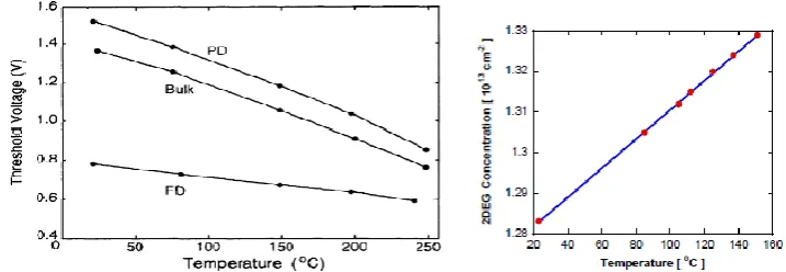
4) Effect of Temperature: The parameters like threshold voltage and mobility are affected with change in the temperature.
For SOI devices as the temperature increases the performance of the device degrades and as temperature
decreases the device performance increases. The mobility and threshold voltage increases as the temperature
decreases, junction leakage current and the off state power consumption decreases.[2] At low temperature,
depletion region expands. Fig 3 shows the graph of temperature verses threshold voltage for SOI devices.
GaN material has wide bandgap so GaN devices can operate at high temperature. The threshold voltage (Vt)
shifts with temperature for GaN fabricated on different substrate. The threshold voltage depends upon design of
epitaxial structure, such as aluminium (AI) mole composition, charge density of (2-Deg) electron gas. At room
temperature, mobility has little degradation with increasing AI content.The temperature graph for GaN devices
is shown in fig 4.
193 | P a g e
5) Process: The fig 5 shows typical GaN fabrication process. It starts with SiC substrate where the buffer channel and barrier is grown. The five basic steps carried out are 1.Device isolation: It is performed by ionimplantation or removal of channel layer. Isolation is necessary for creating RF circuits 2. Ohmic metallization:
It creates the source and drain electrodes. It is done at very high temperature.3.Nitride passivation: After drain
and source are formed, semiconductor is passivated using silicon nitride.4.Nitride opening and gate metal
deposition: Openings are created in silicon nitride and metals are deposited on them, which creates the
gates.5.Additional nitride and metal layers: After several additional layer of nitrides and metals are deposited,
these layers create source filed plates, interconnects and capacitors.
Fig 5: Typical GaN process
Finally the substrate is thinned (typically to 100 micrometer) ,bottom of substrate is metallized and short paths
between the top and bottom of substrate are created.
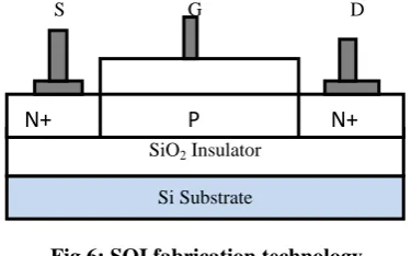
In SOI fabrication technology transistors are build on a silicon layer resting on an insulating layer of silicon
dioxide (sio2).The insulating layer is created by flowing oxygen on to a plain silicon wafer and then heating the
wafer to oxidise the silicon, thereby creating a uniform buried layer of silicon dioxide. Transistors are
encapsulated in Sio2 on all sides.
S G D
Fig 6: SOI fabrication technology.
The insulating layer increases device performance by reducing junction capacitance as junction is isolated from
back silicon. The decrease in junction capacitance also reduces overall power consumption. In SOI the source,
body and drain regions are insulated from substrate. The body is left unconnected and that results in floating
body .The floating body can get freely charge/discharge due to transients (switching) and this affects the
threshold voltage characteristics.
Si Substrate
SiO2 Insulator
194 | P a g e
IV DEVICE PERFORMANCE AS RF CIRCUIT COMPONENT
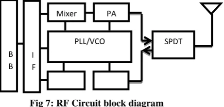
Due to reduced junction capacitance and completely isolated structure, the SOI-CMOS device can be used for
high frequency applications .One such application is shown in the fig 7.The RF circuit block is shown below. A
switch (SPDT) single pole double throw is used to separate the transmission and the reception. It reduces the
signal transmission loss. As the junction capacity is small, it is possible to minimize signal transmission loss
even in high frequency areas. In RF circuits there are passive devices like capacitor and inductors for impedance
matching and frequency selection. As the SOI-CMOS device has complete isolation structure it is possible to
use high resistance substrate as supporting substrate. Passive devices with high frequency characteristics can
also be combined. A one chip transceiver can be developed by combining analog and digital circuits.The major
issue in this case is cross talk. Cross talk can be defined as the electromagnetic disturbance induced by circuit in
another circuit which is located nearby.[10] The cross talk can be divided into two mechanisms. First is injection
into the substrate and second is propagation of noise through the substrate. The parameters involved in
determining substrate cross talk are isolation structure and substrate material.
Fig 7: RF Circuit block diagram
The complete oxide isolation between devices essentially cuts off the direct path of substrate injection noise and
further reduces the capacitive coupling through the substrate .The solution to this is to use high resistance
substrate, which will improve the cross talk characteristics. The buried oxide layer offers a complete isolation
between the active device and the substrate .So a high resistivity substrate can be selected [3]. Once this issue is
solved it is possible to develop mixed signal radio transceiver which will handle higher frequencies in GHz. A
high resistivity substrate also reduces the microstrip loss at high frequency. The microstrip is usually used for
impedance matching.
To reduce the power consumption the supply voltage is to be reduced, which gives rise to CMOS latch up
phenomenon. Latch up is functional chip failure associated with excessive current going through the chip,
caused by weak circuit design. In latch up condition, current flows from VDD to GND directly, causing
dangerous condition of short circuit. Excessive current flows from VDD to GND. In this phenomenon a
parasitic thyristor is generated between power supply and GND pin. The thyristor is activated by internal noise.
So the system malfunctions. This mainly causes when there is rise in temperature and device integration is
improved. In case of SOI CMOS each element is completely isolated by BOX oxide film, so no parasitic SCR is
formed and latch up phenomenon does not occur.
The GaN technology is also used for applications having higher frequencies. The high frequency requirement
and high power makes it necessary to have semiconductor material to have high breakdown voltage and high
electron velocity. To achieve this GaN technology is preferable. For RF application low voltage and high
voltage devices are integrated on the same substrate resulting in the cross talk issues. The major crosstalk lies B
B I F
Mixer PA
PLL/VCO
Mixer LNA
195 | P a g e
with the low voltage devices. Under the influence of high electric field these devices have their charged statechanged due to electron capture emission process, there will be threshold voltage shift and drain current
variations .It is found that grounding the substrate will eliminate the effect of cross talk.[9] In GaN devices latch
up phenomenon is not an issue as minority carriers have very short lifetime in terms of nanoseconds.
V. CONCLUSIONS
This paper reviewed SOI CMOS and GaN MMIC technology based upon certain parameters like device
capability, device structure, characteristics, and effect of temperature on threshold voltage and mobility, and
manufacturing process. The performance of the device as an RF circuit is also evaluated for higher frequencies.
The SOI CMOS device technology provides low power consumption for analog and digital RF mixed circuits in
the design of low power RF transceiver.SOI CMOS is cost effective technology for RF system on chip upto 10
GHz without affecting the performance. Reduction in cross talk and addition of passive components are the key
for SOI CMOS technology. The advantages of GaN technology are its high power density and improved
efficiency. The GaN process operates in different frequency band ranging from 1GHz to 110 GHz.The GaN is
compatible with heterogeneous integration with SOI CMOS.
REFERENCES
[1.] Amrik Singh , Sukhwinder Singh “Evolution of CMOS Technology Past, Present and Future”,
International Journal of Engineering Research & Technology (IJERT), Vol. 5 Issue 02, February-2016
[2.] Neha Goel , Ankit Tripathi “Temperature effects on Threshold Voltage and Mobility for Partially
Depleted SOI MOSFET”, International Journal of Computer Applications (0975 – 8887), Volume 42–
No.21, March 2012.
[3.] Jerry Yue and Jeff Kriz, “SOI CMOS Technology For RF System On Chip Applications ” Honeywell
Solid State Electronics Center Plymouth, MN
[4.] Yasuhiro FUKUDA, Shuji ITO, Masahiro ITO, “SOI-CMOS Device Technology”,Special Edition on 21st
Century Solutions, OKI Technical Review 185,Vol68 ,March 2001
[5.] Umesh K. Mishra, Likun Shen, Thomas E. Kazior, and Yi-Feng Wu”GaN-Based RF Power Devices and
Amplifiers” Vol. 96, No. 2, February 2008 | Proceedings of the IEEE
Kaixue Ma, Shouxian Mou , Kiat Seng Yeo “A Study of CMOS SOI for RF, Microwave and Millimeter Wave Applications” ISOCC 2015,IEEE 2015
[8.] Nicholas J. Kolias,“Recent Advances in GaN MMIC Technology” ,IEEE 2015
[9.] Qimeng Jiang, Zhikai Tang, Chunhua Zhou, Shu Yang,and Kevin J. Chen, “Substrate-Coupled Cross-Talk
Effects on an AlGaN/GaN-on-Si Smart Power IC Platform”, IEEE TRANSACTIONS ON ELECTRON
DEVICES, VOL. 61, NO. 11, NOVEMBER 2014
[10.]Khaled Ben Ali, César Roda Neve, Ali Gharsallah, and Jean-Pierre Raskin “Impact of Crosstalk into High
Resistivity Silicon Substrate on the RF Performance of SOI MOSFET”, Journal of Telecommunication
196 | P a g e
[11.]“Some Recent Trends in RFIC/MMIC Technology”, Technology report , High Frequency Electronics ,July 2005
[12.]“Gallium Nitride (GaN) Technology Overview”, GaN Transistors for Efficient Power Conversion,Copyright EPC 2012
[13.]Satya Sai Srikant “An Overview on Monolithic Microwave Integrated Circuits”, Turkish Journal of
Engineering, Science and Technology ,03 (2014) 123-126
[14.]Balwant Raj and Sukhleen Bindra Narang, “Analysis of AlGaN/GaN based HEMT Device for MMIC
Design” ,International Journal of Advanced VLSI Design ,January-June 2011, Volume 1, No. 1, pp. 11-18
[15.]Steven H. Voldman “CMOS Latchup”, John Wiley & Sons, Ltd,2007