Version 1.1 2 3
Contents
4 1 Introduction 1 52 Analog front-end and variants 4
6 2.1 Front-end overview . . . 4 7 2.2 Analog variants . . . 5 8 3 Region architecture 7 9
4 Configuration and control 7
10
5 Readout 10
11
6 Pinout tables 11
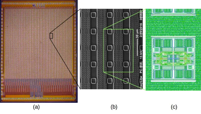
Figure 1: (a) Photograph of FE65-P2. References to bottom, top, left, and right throughout the text assume the orientation in this picture. (b) SEM micrograph showing detail with several bump pads on 50µm pitch visible. The column power bus structure can also be seen. (c) layout detail showing an analog quad island surrounded by synthesized logic.
1
Introduction
13
This document is intended as both a user guide and a design reference to the FE65-P2 chip. The
14
operation description is aimed at non-experts who will use the chip to carry out tests. Many details in this
15
document will already be captured by existing test setup defaults. Descriptions of suitable test setups and
16
software are not included here.
17
The FE65-P2 contains a matrix of 64 by 64 pixels on 50µm by 50µm pitch, designed to read out a
18
bump bonded sensor. It is implemented in 65 nm bulk CMOS and was fabricated in a multi-project run
19
delivered in December 2015. The goals of FE65-P2 are to demonstrate excellent analog performance,
20
isolated from digital activity well enough to achieve 500 electron stable threshold, radiation hard to at
21
least 500Mrad, and to prove the novel concept of isolated analog front ends embedded in a flat digital
22
design, called analog islands in a digital sea. Each analog island is completely surrounded by digital
23
circuitry, which was generated by automated place and route tools and will therefore be different around
24
every island. A digital on top design flow was used, where each “quad column” of 4 by 64 pixels was
25
synthesized as one unit. The chip outline is approximately 3.5 mm by 4.4 mm. Fig. 1 shows a chip photo,
26
a layout view of an analog island, and an SEM image of the bump pad structure. The FE65-P2 design
27
and test results are intended to inform the RD53A chip [1], which will be a large format prototype for the
28
ATLAS and CMS Phase 2 pixel detectors.
29
Every FE65-P2 pixel has a dedicated analog front end, consisting of a charge integrator, followed
30
by a single ended to differential second stage feeding a differential comparator. The front ends are laid
out in compact groups of four or quads (also called analog islands) sharing power and bias distribution.
32
Configuration bits for front end tuning and function selection are stored in the synthesized digital logic
33
and supplied to each front end quad as static CMOS levels. Threshold discrimination is achieved by
un-34
balancing the comparator differential inputs. Two global threshold DAC settings control this unbalancing.
35
There are additionally 5 threshold trim bits in each pixel. The integrator has four gain choices selected by
36
two global bits, and a current source feedback. There is a global adjustment for the feedback current, but
37
no tuning bits on an individual pixel basis. The chip contains several variants for some of the front end
38
details to be optimized, such as the values of the selectable feedback capacitors or presence of a pixel
39
power down bit. Details about the analog front end and all variants are given in Sec. 2.
40
The FE65-P2 chip includes on-chip biasing circuitry, a simple serial programming interface and an
41
output serial link allowing continuous triggering and data taking. The chip configuration has a hard-wired
42
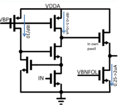
default value allowing standalone analog operation with minimal connections and no need for digital
43
control, as summarized in Table 1. All control I/O not shown in Table 1 can be left unconnected as
44
it contains internal pull-up/down resistors to set the default value. In particular, the 2-bit reset code is
45
internally pulled to zero, which selects the default configuration.
46
For digital data acquisition operation the reset code must be externally controlled and a configuration
47
loaded. It is not possible to use the default configuration of the pixel matrix while exercising the digital
48
data acquisition. The basic digital operation requires just a few inputs and outputs as summarized in
49
Table 2. The pixel matrix readout architecture is based on the FE-I4 region architecture [2] with some
50
modifications, described in Sec. 3.
51
The FE65-P2 power and bias signal distribution have been optimized to minimize coupling and achieve
52
low threshold. A column-based distribution is used for both, which necessarily crosses over “digital sea”
53
in between analog quads. A metal layer is used as shield to prevent digital to analog coupling. All circuits,
54
both analog and digital, are isolated from the substrate using well implant structures, while isolation of the
55
I/O pads relies on a reverse-biased junction. This is why the substrate can be biased away from ground
56
as indicated in Table 1 (this will be done only for special studies).
57
Symbol Function Min Max Comments
VDDD Digital supply voltage (VDDA-0.1) V(∗) 1.2 V min. can be lower for testing
VDDA Analog supply voltage 1.0 V 1.2 V a single supply can be used
DAC Externally supplied 80 nA 120 nA 100 nA nominal. A resistor to
REF master reference current VDDA can be used instead if
VBN (a.k.a Iref) performance is not critical
GNDD Digital supply retrun 0 V 0 V tie to common ground
GNDA Analog supply retrun 0 V 0 V tie to common ground
VSUB substrate contacts <-1 V +0.2 V nominally tie to ground
INJIN Analog inject input 0 V VDDA falling edge injects
OUT xx Source follower pixel outputs 0 V VDDA must pull-up externally
IDDA Analog current consumption 10 mA 18 mA varies with Iref
IDDD Digital current consumption 0 ∼0 mA
capA Analog power decoupling 0.1µF
capD Digital power decoupling 0.1µF
V CTR Feedback cap selection 0 V VDDD must be set- no internal pull-R
CF1/2
Table 1: Minimal requirements for basic analog operation. Power need only be supplied at one set of pads at the bottom of the chip, but multi-pin supply may improve performance. ((∗)The analog quad configuration bits are supplied by the digital without level-shifting. Therefore too low a digital voltage relative to analog could lead to problems.
Symbol In/Out Function Comments
Reset(0) CMOS in reset bit 0 set to 1 for full operation
Reset(1) CMOS in reset bit 1 set to 1 for full operation
SI Config CMOS in shift register in all configuration bits enter here
CLK Config CMOS in shift register clock advances the shift register
SO Config CMOS out shift register out
LD Config CMOS in load global configuration high loads SR contents, low latches
En Pix SR Config CMOS in config. mode set to load pixel column SR
TRIGGER CMOS in trigger gate input gates CLK BX to generate triggers
CLK BX CMOS in bunch crossing clock 40 MHz nominal
CLK DATA CMOS in data output clock Must provide separately from CLK BX.
Up to 320 MHz
CLK BX CMOS in bunch crossing clock 40 MHz nominal
OUT DATA P CMOS output 8b/10b data Yes, CMOS
OUT DATA N CMOS output inverted OUT DATA P Not real differential
2
Analog front-end and variants
58
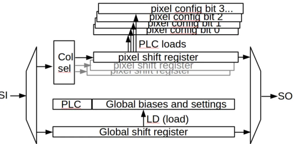
2.1
Front-end overview
59
The building blocks of the main array consist of so-calledquad-islandsof 2×2 pixels with custom analog
60
pads isolated from the substrate hosting bias and power grids. No I/O, memory latches, flip-flops or
coun-61
ters are found in the analog portion of the pixel area; instead, static configuration values are provided by
62
the digital core, which receives a comparator out signal from the analog part. This part is a small-area
63
low-power front-end that has been designed for flexibility and testing. The ADC function is implemented
64
using the time-over-threshold (ToT) principle, which is based on the fact that the comaparator pulse width
65
is related to the amount of charge collected by the pre-amp. This enables evaluation of the charge
col-66
lected by letting the counter in each pixel record the number of clocks for which the pulse remains above
67
the discriminator threshold. The analog pixel just provides the discriminator pulse, while the counting is
68
performed in the synthesized digital core.
69
Bloc diagram of front-end
•Based on the new geometry Cdet of 100fF maximum is assumed.
•Leakage current compensation a la FEI4 (not shown), 10nA nominal
•5b (4b + sign) tuning DAC .
•Few different variants are considered
•Globally settable feedback cap (2bit). CF0/CF1 become CF0’/CF1’ in some variants.
•Target total analog current is <5mA/pixel.
PreComparator Replica preamp Chip-wide CF0 CF1
Figure 2:Block diagram of analog front-end.
When a particle passes through the sensor (diode symbol in the block diagram in Figure 2) it creates
70
a certain amount of electron-hole pairs. These charge carriers will drift towards the charge-sensitive
71
pre-amplifier and induce a signal at the input that it integrated by the amplifier. The pre-amplifier has
72
a simple straight regulated cascode architecture (see Figure 3) in weak inversion and a first stage with
73
continuous reset and adjustable gain through two selectable global bits. The pre-amp can operate at very
74
low currents and has three bias lines. The pre-amp bias, voltage follower and feedback current settings
75
are made through 8-bit global DACs. There is also a programmable injection capacitor (not shown in
76
diagram) for analog calibration connected to the input of the pre-amp.
77
Preamp schematics
IB P =0 .5 ->5 u A 0.25 ->2u A In own pwell IB P/10Simple straight cascode configuration
Could operate at very low currents
Only 2 Bias lines
All devices are isolated from substrate
A mix of transistor flavors
The DC-coupled pre-comparator amplifier stage is also referred to as the differential threshold circuit.
78
It implements threshold setting and tuning and provides additional gain. The global threshold is adjustable
79
through two 8-bit DACs (vthin1 and vthin2) while the individual pixel thresholds can be adjusted by the
80
pseudo-differential configuration of the two pre-comparator outputs that produces a differential signal at
81
the input of the comparator by unbalancing signal levels. The added asymmetry feature of this unique
82
design allows the pixel threshold to be fine-tuned by 4 + sign trim bits where the threshold (in e-) increases
83
as the number represented by these 4 bits increases. The trim bits act on branch 1 or branch 2 of the
84
differential threshold circuit for DTH1 and DTH2 respectively. This is done by threshold tuning DACs
85
(TDACs) which provide a mechanism for making small relative threshold adjustments at the single channel
86
level. The values of DTH1 and DTH2 are set by a single 5-bit pixel configuration register plus a global
87
set bit value as detailed in Table 3. This design is optimized for low-threshold operation and allows the
88
chip to be tested with both positive and negative charge carrier sensors as well as for the total area to
89
be minimized. Other advantages include mismatch reduction and improved power supply rejection. The
90
pre-comparator stage is followed by a classic CT comparator stage with output connected to the digital
91
pixel region through logic gates.
92
Table 3: Truth table for the threshold tuning DACs. If the set bit value is 0 DTH1 will reflect the latch content and DTH2 takes the state of a global default line (0 or 15). If the set bit value is instead 1 DTH2 will reflect the latch content, while DTH1 takes on the default value.
5-bit DAC setting Set bit value DTH1 DTH2
0-15 0 0-15 0
16-31 0 0-15 15
0-15 1 0 0-15
16-31 1 15 0-15
Designed for 500e− threshold operation, the analog pixel has a current consumption of 4 µA/pixel
93
at 50 fF detector load and 10 nA leakage current, but is designed to operate up to 100fF load and 20
94
nA leakage, resulting in higher threshold and/or higher power. Assuming that power is anchored at 4
95
equidistant places, the maximum voltage drop provided by the power lines is∆V∼5 mV for a 336×336
96
array at a current consumption of 5µA per pixel. The target total analog current is below 5µA per pixel.
97
2.2
Analog variants
98
The FE65-P2 array is not completely uniform, but includes multiple circuit variants with varying properties
99
in order to allow for testing and find optimal settings for the chip for different scenarios. At the core
100
level the chip is partitioned into 16 quad columns (each quad column has 4 by 64 pixels), of which there
101
are 8 variants (so there are 4 quad columns of each variety, see Figure 4). How this division has been
102
implemented and specifications for each variant is described in Table 4a.
103
For CPLxx1 columns there is an additional feedback circuit such as the one displayed in the green
104
box in the upper left corner of Figure 2, providing DC leakage current compensation through a low pass
105
filter which increases the feedback gain (see Table 4a). The CPL011 variant is the only one with a power
106
down setting, which is a new feature that has been added to allow powering down the analog activity.
107
There are no feedback current settings for individual pixels; instead, two globally switchable pre-amp
108
feedback capacitances are used. Since this chip is a prototype, the value of these two capacitors can be
109
varied in order to permit optimization for the final version of the chip. The values are set by the two control
110
bits CF0 and CF1 and selected by jumpers on the test board to any combination of low/high referring
111
to leaving the switches connected to the feedback capacitors open/closed respectively (see Table 4a
112
for corresponding capacitor values). It is critical that these jumpers are always set to something (1 or
113
0), because there are not pullup or pulldown resistors on these pads and if left floating the feedback
capacitance can vary randomly. The default baseline setting is to leave both switches open (i.e. CF0 and
115
CF1 both set to low). In this case there will still be a non-zero feedback capacitance given entirely by
116
parasitic capacitance, which is simulated to be ??? and which results in the highest gain.
117
Two of the column variants have an increased gate width of the amplifier PMOS load in order to
118
improve the radiation hardness. These columns are marked ”RH” (see Table 4a).
119
In addition to the column variants, there are also 8 different top row test structures (see Table 4b and
120
pin 90-101 in pinout table 7). These structures are used for injection of DC leakage current and to change
121
the simulated detector capacitance externally with a varactor, which is a tuning diode used as a
voltage-122
controlled capacitor (∼70fF at 0V bias). This solution gives direct access to the buffered pre-amp output
123
and the output between the first and second stage comparators. Each top row output goes to a source
124
follower connected to an external pull-up resistor that can be used for probing the signal. Typical sample
125
waveforms for a 500 mV peak-to-peak injection pulse are displayed in Figure??. (New waveforms to be
126
added.)
127
Table 4:Variant partition.
Variant ID CF0/CF1 [fF] Power Dwn Leakage Comp W (amp2 load PMOS) [µm] Column Double column Quad column
CPL000 3.36/4.99 no no 0.2 0-7 0-3 0-1 CPL001 3.36/4.99 no yes 0.2 8-15 4-7 2-3 CPL011 3.36/4.99 yes yes 0.2 16-23 8-11 4-5 CPL001RH 3.36/4.99 no yes 0.48 24-31 12-15 6-7 CPL100 5.15/7.76 no no 0.2 32-39 16-19 8-9 CPL101 5.15/7.76 no yes 0.2 40-47 20-23 10-11 CPL101RH 5.15/7.76 no yes 0.48 48-55 24-27 12-13 CPL101 5.15/7.76 no yes 0.2 56-63 28-31 14-15
(a)Column information. The binary naming scheme is such that the first digit (C) respresents the feedback capacitor values (low/high), the second digit (P) the power down feature (on/off) and the third digit (L) the leakage current compensation (on/off).
Column Varactor Leakage input
0-1 yes yes 4-5 yes yes 8-9 yes yes 13-14 no yes 14-15 no yes 15-16 no yes 16-17 yes yes 20-21 yes yes
(b)Top row information.
5
9/03/2015 M. Garcia-Sciveres --- FE65-P2 Intro
Chip Layout
I/O and power.
Test pads for power, bias, and top row analog internal signals
T es t p ad s, n ot y et u se d T es t pa ds , n ot y et u se d 64 x 64 pixels 3497µm 44 2 1 µ m C PL 0 0 0 C PL 0 0 1 C PL 0 1 1 C PL 0 0 1 R H C PL 1 0 0 C PL 1 0 1 C PL 1 0 1 R H C PL 1 0 1
3
Region architecture
128
The discriminator output of each pixel is fed into a digital region where the firing time of each discriminator
129
and the 4-bit ToT information is recorded from the counts of an externally supplied clock, with a nominal
130
frequency of 40 MHz. Similar to the architecture of its predecessor FE-I4, the analog pixel matrix of
131
FE65-P2 is divided into units of 2×2 pixels and the digital readout with 25 ns time resolution is based on
132
local hit storage in these quad regions. To deal with the high hit occupancies, each region has its own
133
buffers and stores hit charge (>2GHz/s/cm2) and timing locally for a programmable latency interval (up to
134
10µs) within which it can be retrieved by supplying an external trigger.
135
4
Configuration and control
136
The functionality of the chip is configurable through a serial peripheral interface (SPI) protocol slow control
137
used to access the global and pixel registers (see Table 5 and Table 6 respectively). Threshold and bias
138
values common to all pixels are set by DACs through the 145 bit global shift register. Additionally, each
139
quad column has its own shift register that is 4x64 bits long. Configuration bits get serially clocked into the
140
appropriate shift register and then transferred (loaded) in parallel to the actual configuration memories,
141
which are separate from the shift registers (see Figure 5). There is a load signal (LD) to move bits from
142
the global shift register to the global configuration memory, and 8 load signals to move bits from the pixel
143
shift register to the pixel configuration memories (one load signal per bit). These pixel load signals are
144
not separate inputs to the chip, but are controlled internally by bits in the global configuration. This is why
145
there are two separate load signals for global configuration, so that the pixels can be configured without
146
disturbing the global bias settings.
147
Table 5:Global registers
Start position
(0 loads last) Size (bits) Name Purpose Default value
0 1 TestHit Enable digital injection via LD CNFG pin Set bit
1 1 SignLD Latch sign value into pixels Set bit
2 1 InjEnLD Latch inject enable into pixels Set bit
3 4 TDACLD Latch TDAC bits into pixels 4×Set bit
7 2 PixLD Latch 2 mode bits into pixels 4×Set bit
9 1 Not used
10 1 OneSR Chain all shift registers into one 1
11 1 Not used 0
12 9 Latency Trigger latency (in BX cycles) 400 (decimal)
21 16 ColEnable Enable digital quad columns 0
37 16 ColSREnable Enable quad column shift registers FFFF (hex)
53 4 ColSROut Select which pixel SR is sent to 15 (decimal)
57 8 Not used 0
65 8 PrmpVbp Pre-amp bias 36 (decimal)
73 8 vthin1 Positive discriminator threshold 255 (decimal)
81 8 vthin2 Negative discriminator threhold 0
89 8 vff Pre-amp feedback bias 42 (decimal)
97 8 VctrCF0 Not conncted 0
105 8 VctrCF1 Not connected 0
113 8 PrmpVbnFol Pre-amp follower bias 51 (decimal)
121 8 vbnLcc Leakage current compensation 1(decimal)
129 8 compVbn Comparator bias 25 (decimal)
137 8 preCompVbn Pre-comparator bias 50 (decimal)
Table 6:Pixel registers Default reset
Pixel Bits
state Comment
PixConf [1:0] b11
InjCtrl [0] b1
TDac [3:0] b1111 threshold tuning magnitude Sign [0] b0 sign bit for the
TDAC operation SR (shif reg ff) [0] 1(?) used for digital inject
mask (TestHitEn)
PixConf[1] PixConf[0] HitOrEn HitEn PowerOn
0 0 0 0 0
0 1 0 0 1
1 0 0 1 1
Figure 6:Nominal settings and specifications
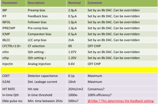
Parameter Description Nominal Comment
IBP Preamp bias 2.0mA Set by an 8b DAC. Can be overridden IFF Feedback bias 0.5mA Set by an 8b DAC. Can be overridden IBFOL Follower bias 1.0mA Set by an 8b DAC. Can be overridden IPRECMP Pre-comp bias 1.0mA Set by an 8b DAC. Can be overridden ICMP Comparator bias 0.5mA Set by an 8b DAC. Can be overridden IBLCC LCC amp bias 2nA Set by an 8b DAC. Can be overridden CFCTRL<1:0> CF selection 00 OFF CHIP
vthn Qth setting - 1.07V Set by an 8b DAC. Can be overridden vthp Qth setting + 1.20V Set by an 8b DAC. Can be overridden InjectIn Analog Injection 0.6V OFF CHIP
CDET Detector capacitance 0.1p Maximum ILEAK Det. Leakage current 10nA Maximum HIT RATE Hit rate 2GHz/cm2 Consensus? In-time Qth In time threshold 1000e- 100% efficiency?
Dble pulse res Min. time between 2hits 500ns? @10ke-? This determines the feedback setting.
Nominal settings and specifications
Figure 7:Configuration settings
Digital Interface
[email protected] 3.09.2015
Name Direction Description
RESET[1:0] input Logic/Default GlobalConf/DefaultPixelConf CLK_BX input BX clock (running continuously)
TRIGGER input trigger, synchronous to CLK_BX, active high
HIT_OR output hit or
CLK_CNFG input clock for configuration
EN_PIX_SR_CNFG input enable for configuring pixels (global<-> pixel SR)
LD_CNFG input load for configuration
SI_CNFG input data input for configuration SO_CNFG output data output for configuration
PIX_D_CONF input selects default state of bits for D (in pixel) CLK_DATA input clock for serial output data
OUT_DATA output output serial data
SPI slow control:
•
pixel register
•
global register
Run mode: is similar to FEI4
5
Readout
148
The digital logic is based on the preceding FE-I4 chip with additional memory to account for the increased
149
hit rate and the digital core is built around the quad-regions, each with 7 memory buffers allowing storage
150
of up to 7 hit arrival times for each region. Further, the digital part is divided into 64×4 super-regions,
151
so-calledquad-columnswith 9-bit BCID memory (2×9-bit Gray counters) distributed for a more constant
152
power consumption and reduced transients by eliminating local latency counters. These quad-columns
153
are replicated 16 times in a step and repeat process to build the 64×64 pixel matrix (see Figure 8).
154
Timon Heim 3 RD53 General Meeting
Digital Layout
Matrix Layout:
• 64x4 pixel matrix organised in “flat” synthesised quad
columns
• Total of 16 quad columns in step & repeat process
• 2x2 pixel share digital region
• 4bit ToT counter, 7 memory locations
• 9bit BCId memory (2x9bit gray counter distributed)
Picture of FE
64x64 pixels
64x4
2x2
End of Column Logic
DACs
Readout
Config
Slow
Control
2x2 not to scalePeripheral Logic:
• End-of-Column logic with token based trigger system
• Serial programming interface to access global and pixel
register
• Up to 320 Mb/s 8b10b encoded readout
Data Flow [email protected] 23.04.2015 4x64 pix el s 4 x6 4 p ix els 4x6 4 pix el s cnt cnt cnt readout cdc fifo framing/8b10b serializer 40MHz clock domain 160/320 MHz clock domain Global signals: - bunch crossing clock- 2x 9bit LatnecyId (distance of latency) - 2x 4bit TriggerId
- trigger
- Readout based on single token for full chip - Support for 16 consecutive triggers - Output data format like FE-I4 24 bit words:
Column, Row, 2xToT
10
Figure 8:FE65-P2 digital layout and data flow.
The end-of-column logic hosts a token based trigger system and a 8b/10b high-speed formatter. The
155
readout is based on a single token for the full chip and supports up to 16 consecutive triggers, with a
156
default trigger rate of 1 MHz and a power consumption of 5.5µW/pixel. The pulse-height information is
157
independently counted for each pixel by applying a digital threshold to the discriminator output prior to
158
starting a dedicated 4-bit binary counter for ToT and using latches to store the distributed counter value.
159
The information retrieved from individual pixels includes the address of the pixel, as well as the charge
160
and timing information about the hit. The 24-bit word output data has the format: column, row, 2×ToT
161
(see Figure 9).
162
Figure 9:Output data format
[email protected] 09/03/15 7 P ix el mapping
FE65_P2 verification updates
Mapping
0 1 2 3 4 5 6 7 8 9 10 11 12 13 14 15 16 17 18 19 20 21 22 23 0
1
n/a n/a Column Row RowP n/a n/a ToT0 ToT1
BCID
To translate the output of the data word into an xy coordinate on the chip:
if( rowP is 1 )
x = 2*column + 1
else
x = 2*column if( ToT0 not 15 ) y = 2*row if( ToT1 not 15 ) y = 2*row + 1
Information about 2 possible hits per word.
64 x 64 pixel matrix Divided into 2x2 digital regions
Outputs 24-bit data word
x
y
The global signals are:
163
• bunch crossing clock
164
• 2×9 bit latency ID (distance of latency)
165
• 2×4 bit trigger ID/trigger request ID
166
• trigger
6
Pinout tables
168
The chip has several test pads along the periphery, which are yet to be routed for power, bias, and top
169
row analog internal signals (see Figure 10). Information about the pinout and pads can be found in Table
170
7 and Table 8 respectively.
171
5 9/03/2015 M. Garcia-Sciveres --- FE65-P2 Intro
Chip Layout
I/O and power.
Test pads for power, bias, and top row analog internal signals
T es t p ad s, n ot y et u se d T es t pa ds , n ot y et u se d 64 x 64 pixels 3497µm 44 2 1 µ m
Figure 10:FE65-P2 pixel matrix structure.
T<0> T<1> T<2> T<3> T<4> T<5> T<6> T<7> T<8> T<9> T<10> T<11> T<12> T<14> T<15> T<16> T<17> TD<1> TD<3> TD<4> TD<6> TD<7> TD<8> TD<9> TD<10> TD<12> TD<13> TD<14> TD<16> TD<2> TD<5> TD<11> IN J IN V S S A _ B D A C _ R E F _ V B N P R E _ C O M P _ V B N C O M P _ V B N P _ R M P _ V B N _ F _ O L V _ C T R _ C F 1 V _ C T R _ C F 0 V F F V T H 1 P _ R M P _ V B P V S S A _ B _ 2 V D D A _ B G N D A _ B V S S A _ B _ 3 V T H 2 O U T _ D A T A N _ P O U T _ D A T A P _ P C L K _ D A T A _ P E N _ P IX _ S R _ C O N F G _ P L D _ C O N F G _ P S I_ C O N F G _ P C L K _ C O N F G _ P T R IG G E R _ P R E S E T _ P < 0 > R E S E T _ P < 1 > C L K _ B X _ P S O _ C O N F G _ P H IT _ O R N _ P H IT _ O R P _ P V B N _ L C C P IX _ D _ C O N F G _ P G N D D V D D D VSSA_R_2 V S S A _ T O P _ 2 C _ B IA S O U T _ 1 _ E X T _ U L 1 3 _ 3 1 GNDD_R_2 VDDD_R_2 VSSA_R GNDD_R VDDD_R V D D A _ T O P G N D D _ T O P V D D D _ T O P V S S A _ T O P O U T _ 1 _ E X T _ U L 8 _ 3 1 O U T _ 2 _ E X T _ U L 8 _ 3 1 O U T _ 2 B _ E X T _ U L 8 _ 3 1 O U T _ 1 _ E X T _ U L 4 _ 3 1 O U T _ 2 _ E X T _ U L 4 _ 3 1 O U T _ 2 B _ E X T _ U L 4 _ 3 1 IN _ B U F F _ C A L O U T _ B U F F _ C A L V B N _ L E A K O U T _ 1 _ E X T _ U L 0 _ 3 1 O U T _ 2 _ E X T _ U L 0 _ 3 1 O U T _ 2 B _ E X T _ U L 0 _ 3 1 O U T _ 2 _ E X T _ U L 1 3 _ 3 1 O U T _ 2 B _ E X T _ U L 1 3 _ 3 1 O U T _ 1 _ E X T _ U L 2 0 _ 3 1 O U T _ 2 _ E X T _ U L 2 0 _ 3 1 O U T _ 2 B _ E X T _ U L 2 0 _ 3 1 O U T _ 1 _ E X T _ U L 1 6 _ 3 1 O U T _ 2 _ E X T _ U L 1 6 _ 3 1 O U T _ 2 B _ E X T _ U L 1 6 _ 3 1 O U T _ 1 _ E X T _ U L 1 5 _ 3 1 O U T _ 2 _ E X T _ U L 1 5 _ 3 1 O U T _ 2 B _ E X T _ U L 1 5 _ 3 1 O U T _ 1 _ E X T _ U L 1 4 _ 3 1 O U T _ 2 _ E X T _ U L 1 4 _ 3 1 O U T _ 2 B _ E X T _ U L 1 4 _ 3 1 G N D A _ T O P VDDA_L GNDA_L VSSA_L VDDA_L_2 GNDA_L_2 VSSA_L_2 VDET T<13> T<18> T<19> TD<0> TD<15> TD<17> TD<18> TD<19> io 0 0io io 0 io 0 io 0 io 0 io 0 io 0 io 0 io 0 0io 0io io 0 0io 0io io 0 io 0 0io io 0 0io io 0 io 0 io 0 io 0 io 0 io 0 io 0 io 0 0io io 0 0io 0io 0io 0io io 0 io 0 io 0 io 0 io 0 io 0 io 0 io 0 io 0 io 0 io 0 io 0 io 0 io 0 io 0 io 0 io 0 io 0 io 0 io 0 io 0 io 0 io 0 io 0 io 0 io 0 io 0 io 0 io 0 io 0 io 0 io 0 io 0 io 0 io 0 io 0 io 0 io 0 io 0 io 0 io 0 io 0 io 0 io 0 io 0 io 0 io 0 io 0 io 0 io 0 io 0 io 0 io 0
FE65 - P2 SCC Symbol
• Many signals for testing — not an actual front end
• 34 signals on top and
bottom
• Top is mostly analog • Bottom is mostly digital
• Next is going from chip to PCB level
Table 7:Pinout information.
Pin# Name Description Pin# Name Description
Left (top→bottom) Right (bottom→top)
1 T<19> NC ESDa 62 VSSA substrate: 0V nominalc
2 T<18> NC ESD 63 GNDD system ground: 0V (=GND)
3 T<17> NC ESD 64 VDDD digital power: 1.2Vi
4 T<16> NC ESD 65 VSSA substrate: 0V nominalc
5 T<15> NC ESD 66 GNDD system ground: 0V (=GND)
6 T<14> NC ESD 67 VDDD digital power: 1.2Vi
7 T<13> NC ESD 68 TD<0> digital hit output; connect to std header pin. Disci out of pixel 63,7b
8 T<12> NC ESD 69 TD<1> NC ESD 9 T<11> NC ESD 70 TD<2> NC ESD 10 T<10> NC ESD 71 TD<3> NC ESD 11 T<9> NC ESD 72 TD<4> NC ESD 12 T<8> NC ESD 73 TD<5> NC ESD 13 T<7> NC ESD 74 TD<6> NC ESD 14 T<6> NC ESD 75 TD<7> NC ESD 15 T<5> NC ESD 76 TD<8> NC ESD 16 T<4> NC ESD 77 TD<9> NC ESD 17 T<3> NC ESD 78 TD<10> NC ESD 18 T<2> NC ESD 79 TD<11> NC ESD 19 T<1> NC ESD 80 TD<12> NC ESD 20 T<0> NC ESD 81 TD<13> NC ESD
21 VDDA analog power: 1.2V 82 TD<14> NC ESD
22 GNDA system ground: 0V (=GND) 83 TD<15> NC ESDa
23 VSSA substrate: 0V nominalc 84 TD<16> NC ESD
24 VDDA analog power: 1.2V 85 TD<17> digital hit output; connect to std header. Disci out of pixel 63,58b
25 GNDA system ground: 0V (=GND) 86 TD<18> digital hit output; connect to std header. Disci out of pixel 63,61b
26 VSSA substrate: 0V nominalc 87 TD<19> digital hit output; connect to std header. Disci out of pixel 63,63b
27 VDET DC LV detector bias
Bottom (left→right) Top (right→left)
28 InjIn analog injection pulse (50Ωto ground) 88 VSSA substrate: 0V nom.c100nF decoupling capsi
29 VSSA substrate: 0V nominalc 89 Cbias Varactor biasd
30 dacRefVbn analog ref. current input (100nA nominal) 90 out1Ext uI20 31 Analog out. Buffered preamp out1 of top row and DCOL 20 left pixel.e
31 preCompVbn pre-comparator bias voltagef 91 out2Ext uI20 31 Analog out. Buffered preamp out2 of top row and DCOL 20 left pixel.e
32 compVbn comparator bias voltagef 92 out2bExt uI20 31 Analog out. Buffered preamp out2b of top row and DCOL 20 left pixel.e
33 vbnLcc leakage compensation amp bias voltagef 93 out1Ext uI16 31 Analog out. Buffered preamp out1 of top row and DCOL 16 left pixel.e
34 PrmpVbnFoI pre-amp follower bias voltagef 94 out2Ext uI16 31 Analog out. Buffered preamp out2 of top row and DCOL 16 left pixel.e
35 VctrCF1 logic level control feedback pre-amp capg 95 out2bExt uI16 31 Analog out. Buffered preamp out2b of top row and DCOL 16 left pixel.e
36 VctrCF0 logic level control feedback pre-amp capg 96 out1Ext uI15 31 Analog out. Buffered preamp out1 of top row and DCOL 15 left pixel.e
37 vff pre-amp feedback bias voltagef 97 out2Ext uI15 31 Analog out. Buffered preamp out2 of top row and DCOL 15 left pixel.e
38 vth2 global threhold control voltage V-h 98 out2bExt uI15 31 Analog out. Buffered preamp out2b of top row and DCOL 15 left pixel.e
39 vth1 global threhold control voltage V+h 99 out1Ext uI14 31 Analog out. Buffered preamp out1 of top row and DCOL 14 left pixel.e
40 PrmpVbp pre-amp main bias voltag?? 100 out2Ext uI14 31 Analog out. Buffered preamp out2 of top row and DCOL 14 left pixel.e
41 VSSA substrate: 0V nominalc 101 out2bExt uI14 31 Analog out. Buffered preamp out2b of top row and DCOL 14 left pixel.e
42 VDDA analog power: 1.2Vi 102 GNDA system ground: 0V (=GND)
43 GNDA system ground: 0V (=GND) 103 VDDA analog power: 1.2Vi
44 VSSA substrate: 0V nominalc 104 GNDD system ground: 0V (=GND)
45 GNDD system ground: 0V (=GND) 105 VDDD digital power: 1.2Vi
46 VDDD digital power: 1.2Vi 106 VSSA substrate: 0V nominalc
47 PIX D CONF p default pixel config. setting. CMOS INPUTj 107 out1Ext uI13 31 Analog out. Buffered preamp out1 of top row and DCOL 13 left pixel.e
48 EN PIX SR CNFG p enable/disable pixel (array) config. shift register 108 out2Ext uI13 31 Analog out. Buffered preamp out2 of top row and DCOL 13 left pixel.e
49 RESET p<0> RESET bit 0k 109 out2bExt uI13 31 Analog out. Buffered preamp out2b of top row and DCOL 13 left pixel.e
50 RESET p<1> RESET bit 1k 110 out1Ext uI8 31 Analog out. Buffered preamp out1 of top row and DCOL 8 left pixel.e
51 LD CNFG p config. shift register LOAD command; Pulled down; CMOS INPUT 111 out2Ext uI8 31 Analog out. Buffered preamp out2 of top row and DCOL 8 left pixel.e
52 SI CNFG p config. shift register data input; Pulled down; CMOS INPUT 112 out2bExt uI8 31 Analog out. Buffered preamp out2b of top row and DCOL 8 left pixel.e
53 CLK CNFG p config. shift register clock; Pulled down; Pulled down; CMOS INPUT 113 out1Ext uI4 31 Analog out. Buffered preamp out1 of top row and DCOL 4 left pixel.e
54 SO CNFG p config. shift register outputl 114 out2Ext uI4 31 Analog out. Buffered preamp out2 of top row and DCOL 4 left pixel.e
55 TRIGGER p trigger pulse; Pulled down; CMOS INPUT 115 out2bExt uI4 31 Analog out. Buffered preamp out2b of top row and DCOL 4 left pixel.e
56 CLK BX p BCO clock; pulled down; CMOS INPUT. Main system freq. 40MHz nom. 116 inBuffCal Analog input to the calibration buffer used for the out signals 57 HIT ORP p The OR of all chip hits (positive)m 117 outBuffCal Analog output of the calibration buffer. Must be pulled up to VDDA.
58 HIT ORN p The OR of all chip hits (negative)m 118 vbnLeak Analog DC current injection inputn
59 CLK DATA p DATA CLOCK; Pulled down; CMOS INPUT; 160MHz nom. (320MHz max.) 119 out1Ext uI0 31 Analog out. Buffered preamp out1 of top row and DCOL 0 left pixel.e
60 OUT DATAP p DATA OUTPUT (positive)o 120 out2Ext uI0 31 Analog out. Buffered preamp out2 of top row and DCOL 0 left pixel.e
61 OUT DATAN p DATA OUTPUT (negative)o 121 out2bExt uI0 31 Analog out. Buffered preamp out2b of top row and DCOL 0 left pixel.e
aConnected to ESD diodes only, NOT connected at PCB level. Should be connected to standard header pin. Not functional
signal.
b(0,0) is the lower leftmost pixel and (63,63) is the upper rightmost pixel. cDo not connect to ground.
dVaractor simulates input capacitance for few select pixel on top row. See suggested PCB schemtaics.
eMust be pulled up to VDDA. See suggested PCB schematics. DCOL=double column. Pull up resitor is 750Ωnominal for all
out1Ext ulxx 31 and 1.5 kΩnominal for all out2xExt ulxx 31.
f100nF to ground. Lemo connector (to force current only if necessary). gVDDA-signal-GND 3 std header pins.
h100nF to ground. Lemo connector (to force voltage only if necessary).
iNeeds decouplig caps to gnd. 4.7µF//100nF as close to chip as possible, 10nF close to every VDDx pad recommended. jSee the configuation sheet and RESET p<0>and RESET p<1>.
kPulled down; Pulled down; CMOS INPUT. See pad information in Table 8. lResistor in series recommended to reduce noise.
mCMOS OUTPUT (”differential”). Resistor in series recommended to reduce noise (value emprical≤100Ω, start with 0Ω). Trace
and load of HIT ORP p and HIT ORN p must be matched.
nTo simulate leakage current for few select pixels. 100nF to gnd.
oCMOS OUTPUT (”differential”). Resistor in series recommended to reduce noise (value emprical≤100Ω, start with 0Ω). Trace
Table 8:Pad information.
Name Direction Quantity Position (0=leftmost) Description
Digital
domain
RESET[1:0] input 2 2, 3
CLK BX input 0 9 BX clock (running continously)
TRIGGER input 2 8 trigger, synchronous to CLK BX, active high
HIT OR output 2 10,11 hit or
CLK CNFG input 1 6 clock for configuration
EN PIX SR CNFG input 1 1 enable for configuring pixels
LD CNFG input 1 4 load for configuration
SI CNFG input 1 5 data input for configuration
SO CNFG output 1 7 data output for configuration
PIX D CNFG input 1 0 selects default state of bits for D (in pixel)
CLK DATA input 2 12 clock for serial output data
OUT DATA output 2 13, 14 serial output data
InjIn input 1 (dynamic)
PrmpVbp input/output 1 vth1 input/output 1 vth2 output/output 1 vff input/output 1 VctrCF0 input 1 (digital/analog) VctrCF1 input 1 (digital/analog) PrmpVbnFoI input/output 1 vbnLcc input/output 1 compVbn input/output 1 preCompVbn input/output 1 Analog/mix ed domain dacRefVbn input 1 Other
VDDA 2 analog positive supply
GNDA 2 analog ground
VSSA (1) 2 analog negative supply
VDDD 2 digital supply GNDD 2 digital ground