DESIGN AND IMPLEMENTATION OF HIGH SPEED
TRIPLE THRESHOLD VOLTAGE BUFFER WITH
SKEWED INPUT AND OUTPUT
Mrs.B.Karthikajothy
1, Mr.M.Thiruppathiraja
2, Mrs.A.Kamatchi Devi
3M.E
1,2, Assistant Professor
2,
Department of Electronics and Communication,
Theni Kammavar Sangam College of Technology, Theni (India)
ABSTRACT
As early the buffer design is done using conventional static CMOS. Most of power dissipation in CMOS
structure is caused by charging or discharging the output load and by the short circuit current that flows from
the power supply to the ground during switching. By using conventional static CMOS buffer design power and
delay optimization is achieved by slightly increasing threshold voltage. As threshold voltage increased beyond
0.4 vdd propagation delay also gets increased. Further propagation delay can be compensated by slight increase
in the number of buffer stage. While increasing number of stages area of the circuit gets increased. To overcome
these aspects skewed inverters are designed as proposed system. From this design power dissipation,
propagation delay and area also gets reduced. These aspects are achieved by varying threshold voltage of
circuit given. Using this design type buffers in the logic circuit clock skew problem is overcome.
Keyword: Vdd-Supply Voltage, CMOS-Complementary Metal Oxide Semiconductor Device.
I. INTRODUCTION
Buffer is an temporary storage element. In electronics, it is an electronic circuit where primary function is to
connect high impedance source to low impedance load without significant distortion in signal. It is applied in
analog circuits to minimize loss of signal strength due to excessive loading of output nodes. It is an unity gain
amplifier. Buffer amplifier is one that provides electrical impedance matching transformation from one circuit to
another.
Voltage buffer transfer voltage from high output impedance to low input impedance, here voltage level of the
circuit remains constant then current level is varied. Current buffer transfer current from low output to high
input impedance, here current level of the circuit remains constant then voltage level is varied.
Many techniques have been employed to reduce power dissipation in VLSI circuits. Lowering the supply
voltage vdd is the most effective to decrease the power dissipation, since CMOS power quadratic- ally depends
on vdd. However low vdd requires low threshold voltage but the sub-threshold leakage power increases
exponentially. Hence there is a great necessity to optimize vth to achieve the required performance at minimum
The existing methods of buffer design are designed using conventional static CMOS. This model dissipates less
power because short circuit component of power is eliminated in the design by tri-stating its output node before
every output signal transition. This is achieved by applying the gate driving signal of
PMOS to NMOS and NMOS to PMOS of the output stage through a feedback network which delays the driving
signal and avoids simultaneous turn on of NMOS and PMOS transistor during signal transition which is the very
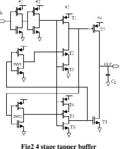
cause of short circuit current. The N stage tapper buffer are given below
Fig 1 N stage tapper buffer
Power and delay optimization is achieved by slightly increasing threshold voltage. Threshold voltage vth should
be in between 0.2vdd and 0.4vdd gives highest reduction in power with a minimal penalty in delay. Propagation
delay gets increased as threshold voltage increased beyond 0.4vdd.threshold voltage value should be less than the
switching threshold that is vm=0.5vdd. Further propagation delay can be compensated by slight increase in the
number of buffer stage.4 stage tapper buffer is shown below
Fig2 4 stage tapper buffer
While increasing number of buffer stage area also get increased. Area, power consumption and delay are not
reduced as we needed so this will be an drawbacks of existing system.Another method is tapered vth approach to
design energy efficient CMOS buffer. In this the energy consumption due to leakage is reduced by tapering the
threshold voltage throughout the buffer stage other than tapering transistor size. The threshold voltage is
reduced progressively when going from the last to the first stage. This enables a considerable leakage in the last
stage at the price of higher delay. The resulting delay penalty is then compensated by reducing the transistor
In high speed application CMOS buffer are typically designed according to the tapered topology where the size
of each inverter of the buffer is a multiple of the previous one.To overcome these drawbacks proposed work of
buffer design are done using triple threshold voltage with skewed input and output which will reduce area,
power and delay.
II.EXISTING SYSTEM
Inverter designed using conventional static CMOS method uses standard threshold voltage. From this
propagation delay is increased. To reduce this delay numbers of stages of inverters are increased, then power
also get reduced but area will get increased. Inverter chains are used in the application of large circuits where
clock skew is considered. Buffers are simply the inverted operation of inverters that is the inverted input is
produced in the output.
Fig3 Inverter circuit
Fig4 Simulated result of inverter using HSPICE simulator
Fig6 Simulated result for inverter chain using HSPICE simulator
Buffer circuit and its chain operations is in opposite of inverter and its chain. From this method some drawbacks
are obtained they are increased number of stages provide area consumption. On increasing threshold voltage
above standard vth power got reduced but propagation delay is increased.
III.PROPOSED SYSTEM
Skewed inverter is proposed are provided with TSMC 90nm model CMOS technology in high vth of about 3vth.
Symbol of skewed IO cell is given below.
Fig7 cell Symbol of the skewed IO
3.1 Operation of skewed IO cells
Skewed IO cells consist of pairs of PMOS and NMOS transistors it is shown in fig8. Unlike conventional static
CMOS it is not driven by same input. Skewed IO cells have two inputs PIN and NIN and two output POUT and
NOUT. It consists of two PMOS transistors P1 and P2 and then two NMOS transistors N1 and N2. The first
output POUT is connected to the drains of P1 and N1. The second output NOUT is connected to the drains of P2
and N2. P1, P2, N1 and N2 have different threshold voltage to trade off circuit speed with power consumption.
Standard vth P2 and N1 are employed to maintain high switching speed in a skewed IO cell. Alternatively high
Fig8 Proposed skewed IO cell
Proposed skewed IO cell is simulated using HSPICE simulator in 90nm model is shown below.
Fig9 Simulation result for skewed inverter
3.2 Two stage buffer
As like inverter cell shown earlier buffer is also designed. Two stage skewed buffer is given below. In this two
skewed buffers C1 and C2 are connected serially which has two pair of outputs as POUT1, POUT2 and
NOUT1, NOUT2.
Fig10 Two stage skewed buffer
Fig11 Simulation result for 2 stage skewed buffer
From this skewed buffer stages clock skew problem is controlled in large circuit. Propagation delay is reduced
while providing separate input to the circuit. Further power also got reduced.
IV. RESULT COMPARISONS
Power, delay and PDP are measured through the simulator by generating netlist. Comparison of result produced
by existing and proposed system is given. From this we can see that power, delay and PDP are reduced on
comparing with existing.
Circuit Power
(µW) Delay (ns) PDP (FJ) Inverter chain
68.591 0.079217 5.43357
Skewed
inverter
33.630 0.011533 0.38786
Fig12 Comparison table for existing and proposed system
V.CONCLUSION
From this paper we can conclude that by using skewed buffers area delay and power is reduced on comparing
with static CMOS design buffer. Probably clock skew problem is reduced while using skewed buffers. On using
this buffer we can design combinational and sequential circuit.
REFERENCES
[1] Ahmed S. And Ismail Y.(2007), Variable Threshold Voltage Design Scheme for CMOS Tapered Buffers,
IEEE International Symposium, pp. 1385 – 1388.
[2] Ankur S. and Payal K.(2013), Design of CMOS Tapered Buffer for High Speed and Low Power
Applications using 65nm Technology, International journal of science and research.
[3] Brian S. C. and Eby G. F. (1995), Design of Tapered Buffers with Local Interconnect Capacitance, IEEE
[4] Brian S. C. and Eby G. F. (1994), Unification of speed, power, area and reliability in CMOS buffer design,
IEEE TRANSACTION.
[5] Frustaci, F. and Corsonello P. (2011), Tapered-VTH CMOS Buffer Design for Improved Energy Efficiency
in Deep Manometer Technology, IEEE TRANSACTION
[6] Maekawa T., Amakawa S., Ishihara N. and Masu K. (2009),Design of CMOS
inverter-based output buffers adapting the cherry-Hooper broad banding technique, ECCTD. pp no.5275025·
[7] Payam H. and Ravindran M. (2004), Design of Ultrahigh-Speed Low-Voltage CMOSCML Buffers and
Latches’, IEEE TRANSACTIONS ON VERY LARGE SCALE INTEGRATION (VLSI) SYSTEMS,
VOL. 12, NO. 10.
[8] Sadhana S. and Shyam A. (2013), Class-AB CMOS Buffer with Low Power and Low Leakage Using
Transistor Gating Technique, International Journal of Advanced Science and Technology, Vol.58, pp.1-12.
[9] Volkan K., Sherif A. T., and Zhiyu L. (2007), Leakage-Aware Design of Manometer SoC, IEEE
TRANSACTIONS.
[10]A. Shebaita and Y. Ismail, Multiple threshold voltage design scheme for CMOS tapered buffers, IEEE
Trans. Circuits Syst—II: Express Briefs, vol. 55,, no. 1, pp. 21–25, Jan. 2008.
[11]S. R. Vemuru and A. R. Thorbjornsen, Variable-taper CMOS buffer, IEEE J. Solid-State Circuits, vol. 26,
no. 9, pp. 1265–1269, Sept. 1991.
[12]S. R. Vemuru and E. D. Smith, Split-capacitive load variable taper buffer design, in Proc. IEEE Midwest