Volume 2006, Article ID 93712, Pages1–12 DOI 10.1155/WCN/2006/93712
Modeling and Characterization of VCOs with
MOS Varactors for RF Transceivers
Pedram Sameni,1Chris Siu,2Shahriar Mirabbasi,1Hormoz Djahanshahi,3Marwa Hamour,1 Krzysztof Iniewski,2and Jatinder Chana3
1Department of Electrical and Computer Engineering, University of British Columbia, Vancouver, British Columbia, Canada V6T 1Z4 2Department of Electrical and Computer Engineering, University of Alberta, Edmonton, Alberta, Canada T6G 2V4
3PMC-Sierra, Burnaby, British Columbia, Canada V5A 4X1
Received 1 September 2005; Revised 8 March 2006; Accepted 17 May 2006
As more broadband wireless standards are introduced and ratified, the complexity of wireless communication systems increases, which necessitates extra care and vigilance in their design. In this paper, various aspects of popular voltage-controlled oscillators (VCOs) as key components in RF transceivers are discussed. The importance of phase noise of these key blocks in the overall performance of RF transceivers is highlighted. Varactors are identified as an important component of LC-based oscillators. A new model for accumulation-mode MOS varactors is introduced. The model is experimentally verified through measurements on LC-based VCOs designed in a standard 0.13μm CMOS process.
Copyright © 2006 Pedram Sameni et al. This is an open access article distributed under the Creative Commons Attribution License, which permits unrestricted use, distribution, and reproduction in any medium, provided the original work is properly cited.
1. INTRODUCTION
In the recent years, the demand for wireless communica-tions has increased considerably. Wireless communication systems encompass a wide variety of standards. Such systems include cellular phones (e.g., GSM, CDMA), wireless local area networks (WLANs), wireless personal area networks (WPANs), wireless metropolitan area networks (WMANs), and so forth. The adoption of any of these technologies de-pends on many variables such as cost and market demand. Over time, the implementation cost of the technologies goes down, which further accelerates their adoption. The high-tech market research firm, In-Stat, forecasts that the world-wide wireless market will grow to more than 2.3 billion sub-scribers by 2009.
Typical RF transceivers have a built-in frequency syn-thesizer, namely local oscillator (LO), to generate a signal with the desired frequency used for up and down conver-sions. Wireless standards strictly specify the minimum level of the received signal, the maximum level of unwanted sig-nal, the channel bandwidth, and the spacing between two ad-jacent channels. Using these specifications and targeting the required signal-to-noise ratio (SNR) after downconversion, the maximum amount of acceptable phase noise on the LO can be calculated. This procedure is conceptually depicted in
Figure 1for the GSM-1800 standard. Using the information provided in the figure and knowing the desired SNR (e.g., 9 dB after downconversion), the maximum acceptable phase noise at 600 kHz offset from the carrier (which is at the cen-ter of the adjacent channel) is calculated to be 121 dBc/Hz [1].
Figure 2 illustrates the problems that may arise if the LO spectrum extends to the adjacent channel with relatively high-power spectral density: after downconversion, there will be an overlap between the spectra of the desired signal and the unwanted adjacent channel. Unless a special tech-nique is used, the recovery of the data becomes almost im-possible.
LOs are usually in the form of voltage-controlled oscil-lators (VCOs) and are placed inside a feedback loop as part of a phase-locked loop (PLL) system. As a result, they con-stantly align their zero-crossings with the reference clock. The amount of generated phase noise, within the bandwidth of the PLL, can be reduced by the loop characteristics.Table 1 compares the maximum allowable phase noise of some of the wireless standards at their nominal frequencies.
Unwanted signal of the adjacent channel with maximum of 43 dBm
Desired channel with minimum allowable GSM
signal of 102 dBm
Unwanted signal of the adjacent channel
White noise floor
200 KHz 200 KHz
1.8 GHz
600 KHz
200 KHz Figure1: GSM channel around 1.8 GHz.
Unwanted signal in the adjacent channel
Desired signal overlaps with interference after
downconversion
Desired signal
Local oscillator (LO)
fLO
fRF LO
fRF
Figure2: Channel interference in the case of larger-than-expected phase noise.
filter, voltage-controlled oscillator (VCO), reference, and feedback divider blocks (/Mand /N). The output frequency of the block isN/Mtimes the reference frequency. Therefore, by adjusting the N/M ratio, different multiples (integer or fractions) of the reference frequency can be generated.
The phase transfer function from the reference to the output of this system exhibits a lowpass characteristic. As a result, high-frequency phase noise1 of the reference clock is attenuated by the loop, while its low-frequency (close-in) noise passes through the system to the output. On the other hand, phase jitter of the VCO will see a high-pass function to the output, which means that low-frequency jitter of the VCO is suppressed within the bandwidth of the phase-locked system.
The total output phase noise is a function of the phase noise of each of the PLL blocks, the input phase noise gener-ated by the reference clock, and noise shaping characteristics of the loop. While there are different techniques for optimiz-ing the performance of the synthesizers to reduce the total phase noise, VCO plays a key role in total phase noise of the system. This is because high-frequency perturbation on the VCO control line tends to appear at the output in the form of phase variations. In addition, any high-frequency (a.k.a. out-of-band) phase noise generated by the VCO due to supply, substrate, or device noise cannot be suppressed by the loop and directly travels to the output. In this paper, our main fo-cus will be on VCO as a key block of RF transceivers.
1The time-domain counterpart of phase noise is jitter, which is a more common term in wireline applications.
Frequency synthesizer circuits have been predominantly implemented in technologies such as III-V, silicon bipolar, or SiGe BiCMOS due to their high-speed and low-noise char-acteristics. However, circuits implemented in these technolo-gies are still expensive, and are not very area efficient. More-over, they are not suitable for system-on-chip integration. Recent advances in CMOS technologies have made CMOS an attractive alternative for implementing high-speed systems, including their oscillators. Advantages of CMOS implemen-tation include lower cost, higher manufacturing yield, lower power, and higher levels of integration, with the possibility of integrating analog and digital circuits on the same chip. Therefore, there is a growing trend in industry to extend the use of CMOS circuits to high-speed integrated digital and mixed-signal systems, on-a-chip (SoC), and system-in-a-package (SiP) designs. However, designing high-speed mixed-signal circuits (e.g., multi-gigahertz systems) in ad-vanced CMOS technologies is very challenging. Issues such as speed, substrate noise coupling, reduced voltage head-room, and increased leakage current pose many difficulties in the design of high-speed CMOS circuits.
Table1: Comparison between phase noises of different wireless standards.
Wireless standard Frequency Phase noise
GSM
850 850 MHz 121 dBc/Hz at 600 KHz
900 900 MHz 121 dBc/Hz at 600 KHz
1800 1800 MHz 121 dBc/Hz at 600 KHz [1]
1900 1900 MHz 121 dBc/Hz at 600 KHz
WLAN
802.11a 5 GHz
Many WLAN transceivers specify “integral” noise in degrees rms over a frequency range, for example, integral of phase noise from 10 K
802.11b 2.4 GHz to 10 M<1.2
Æ
rms for the whole TX path, or 0.8Æ
rms for the synthesizer. This may also be
802.11g 2.4 GHz
translated to an average phase noise spec, like P.N.< 90 dBc/Hz at<100 KHz
(in-band, or close-in)
WPAN ZigBee (802.15.4)
900 MHz
95 dBc/Hz at 5 MHz 2.4 GHz
Bluetooth (802.15.1) 2.4 GHz 94 dBc/Hz at 100 KHz [2]
Crystal osc. Phase/
freq. detector
Charge pump
Lowpass filter
M
N VCO
Output Ref.
Figure3: A block diagram of a frequency synthesizer.
relationship with the C-V curve of varactors. A new practical model for accumulation-mode MOS varactors is then intro-duced. Experimental results follow inSection 4and conclud-ing remarks inSection 5.
2. COMPARISON OF POPULAR VCO ARCHITECTURES
VCOs are one of the main building blocks of RF transceivers. They are utilized inside PLL-based circuits (e.g., frequency synthesizers as part of LO) to generate a clean and low-jitter clock signal for the operation of other blocks of the frequency synthesizer or transceiver. Typical oscillator circuits require some form of positive feedback around a gain stage in or-der to sustain their oscillation. This concept is illustrated in Figure 4. The closed-loop system (oscillator) has to fulfill the following two Barkhausen conditions at all times for contin-uous oscillation:
H(jω)1,
∠H(jω)=360Æ
. (1)
Three common categories of oscillator circuits are relax-ation (Figure 5), ring (Figure 6), and LC-based (Figure 7)
os-Vin +
+
+ H(s) Vout
Figure4: A gain stage with a positive feedback loop.
VDD
R1 R2
M1 M2
C
Itune
Figure5: Relaxation oscillator.
Inverters with controllable
delay
Figure6: Ring oscillator.
can also be adjusted by digitally adding or removing inverters from the chain (coarse tuning). On the downside, the ring and relaxation oscillators suffer from a poor frequency sta-bility, which manifests itself as higher phase noise.
LC-based oscillators are usually made with a diff eren-tial pair amplifier, using LC tank as the load. By connect-ing the outputs to the inputs, the amplifier starts to am-plify the noise at its inputs around the resonance frequency of the tank, provided that its open loop gain is greater than one (first of the two Barkhausen conditions). Noise at other frequencies gets filtered out by the LC tank. This filtering characteristic of LC-based oscillators has made them the best in terms of phase-noise performance. Furthermore, com-pared to the other two oscillator architectures, LC oscillators typically operate more reliably at higher frequencies, pro-vided an LC tank of moderate- to high-quality factor. How-ever, they suffer from their inherently narrower tuning range. Moreover, the integration of LC-based oscillators is more costly due to the large space allocated to on-chip inductors. It should be noted that, as technology advances, achieving higher frequencies becomes more feasible, which in turn re-quires smaller (less spacious) inductors.Table 2summarizes the advantages and disadvantages of the three oscillator ar-chitectures [3].
3. LC-BASED VCOs
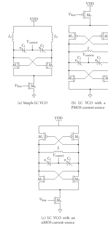
Figure 7illustrates three forms of typical LC VCO implemen-tations in CMOS.Figure 7(a)represents the simplest imple-mentation, with an nMOS current source and an nMOS
dif-VDD
L1 L2
C1 C2
M1 M2
M0
Vbias
Vcontrol
(a) Simple LC VCO
VDD
Vbias M0
M1 M2
M3 M4
C1 C2
Vcontrol
L
(b) LC VCO with a PMOS current source VDD
Vbias M0
M1 M2
M3 M4
C1 C2
Vcontrol
L
(c) LC VCO with an nMOS current source
Figure7: Different versions of LC-based oscillator.
ferential pair as the gain stage (also referred to as “negative resistance”), which cancels out the loss of the tank. A pair of varactors has been used for frequency tuning. The use of differential signaling is another advantage compared to single-ended VCOs (e.g., ring oscillator inFigure 6). It results in higher oscillation swing in a constantly shrinking supply voltage environment, and less susceptibility to environmen-tal noise due to rejection of the common-mode component of the noise.
Table2: Comparison of existing popular oscillator architectures [3].
LC oscillator Ring oscillator Multivibrator
Speed Technology dependent (0.01–10 s of GHz)
Phase noise Good Poor
Integration Poor (inductor and varactor) Excellent
Tunability Narrow/slow Wide/fast
Stability Good Poor (needs acquisition aid with a PLL)
oscillation waveform is symmetrical (i.e., equal rise and fall times), the DC component of the phase noise gets elimi-nated, which is the component that also carries flicker (1/ f) noise. As a result, the two architectures shown in Figures7(b) and7(c)potentially have lower phase noise compared to the architecture inFigure 7(a), which has asymmetrical rise and fall times. The use of nMOS or pMOS current sources cre-ates a level of shielding between substrate (ground) or power supply (VDD), respectively, which subsequently lowers the phase noise due to substrate or supply noise. In technolo-gies where larger supply voltages are available, using voltage regulators is recommended for the VCO to further reduce the oscillator phase noise resulting from substrate and sup-ply noise.
Other than noise components contributed by the os-cillator’s active elements (as well as supply and substrate), there are other sources of noise resulting from the losses in nonideal passive elements (inductors and varactors), which further degrade the overall phase noise performance of the LC oscillator. To reduce the noise floor due to the lossy in-ductors, inductors with higher quality factors (Q) need to be used, since they result in lower resistive loss and subse-quently lower thermal noise and lower power dissipation. To some extent, however, this is limited by the technology, as the thickness of the metal layers and substrate losses are technology dependent, leaving the designer with fewer de-grees of design freedom (e.g., increasing the width of induc-tor wires to lower the loss would degrade the self-resonance frequency). Various solutions are limited by other criteria, such as silicon-area usage. Although design of high-Q on-chip inductors is a topic of active research, our focus in the following sections remains on varactors as the tuning ele-ment of LC VCOs. The design, characterization, and mod-eling of the varactors significantly affect the overall perfor-mance of the LC VCO.
3.1. Varactors
Varactors are a principal component of LC VCOs used for frequency fine tuning. Digitally controlled switched varac-tors or switched capacivarac-tors could also be used for coarse tun-ing in some designs. Traditionally, reversed-biased pn junc-tion diodes acted as the varactor for LC VCOs (this is still true in the case of bipolar VCOs). However, MOS-based varactors are gaining popularity over the reverse-biased diodes due to wider tuning range and higherQfactor, both of which im-prove with every new process generation. Higher doping lev-els in silicon, which in turn result in lower resistive losses
A B
Figure8: An nMOS transistor configured as a varactor.
and lower phase noise, have driven this improvement. It has become more evident in recent designs in advanced CMOS technologies (e.g., 0.18μm, 0.13μm, 90 nm) as implementa-tion of monolithic high-speed VCOs becomes feasible.
An nMOS varactor can have the same structure as an nMOS transistor, with gate as the first terminal and drain, source, and bulk connected together to form the second ter-minal (Figure 8). MOS varactors operate in four main re-gions, based on the biasing point (voltage across the var-actor terminals): accumulation, depletion, weak inversion, and strong inversion. Accumulation and strong inversion are two regions where most varactors are designed to op-erate in. Furthermore, a study on accumulation-mode and inversion-mode varactors reveals that LC oscillators based on accumulation-mode varactors demonstrate lower power consumption and lower phase noise at large offset frequen-cies from the carrier, compared to those based on strong in-version varactors [5].
In most applications, designers would like to ensure that the capacitance of the varactor is a monotonic function of the biasing voltage. For instance, in an LC VCO, it would be de-sirable, as mentioned earlier, to have the varactor operating predominantly in accumulation mode. However, using a reg-ular nMOS, as inFigure 8, does not warrant this, as the oper-ation region is voltage dependant. It is also worth noting that the C-V curve of a regular nMOS is frequency dependant. Figure 9illustrates the cross-section of a varactor structure. It may seem similar to an nMOS transistor, however, then+ regions have been buried inn-well, instead of p-well. This configuration guarantees that the device does not enter the inversion-mode at all; hence the name accumulation-mode MOS (AMOS) varactor.
Sub
Gate (G)
Bulk (B)
p+ n+ n-well n+
p-substrate
Figure9: Cross-section of an accumulation-mode MOS (AMOS) varactor.
However, measuring subpico Farad capacitances is difficult and requires a fairly expensiveS-parameter RF measurement setup. It is, therefore, very useful to predict the tuning char-acteristics of LC oscillators using standard foundry-supplied models for MOSFETs.
Recently, a lot of effort has been expended on modeling the C-V characteristics of MOS varactors, partly due to the increasing popularity of CMOS LC VCOs in which such var-actors are used. One type of model is based on physically meaningful parameters [6] that describe the characteristics of the device with different equations for different regions of operation. Another model based on the physical param-eters of the device is reported in [7]. However, simulating and using these types of models are not simple in SPICE or similar simulators, as they require defining mathematical functions inside the tool. Other models have been developed based on subcircuits utilizing BSIM SPICE models [8]. These models are suitable for simulator implementation within the circuit-design environment and could be easily adopted for future technologies. In the following sections, we introduce a SPICE-like model that takes advantage of already developed foundry models of transistors to create a practical model for accumulation-mode varactors. First we take a closer look at the tuning characteristics of LC VCOs, which further empha-sizes the need for a good varactor model.
3.2. VCO design and tuning characteristics
For the following analysis, we used a standard LC VCO cir-cuit with current source isolating the core of the oscillator from the ground, as shown inFigure 7(b). The structure is designed for 5–6 GHz operation. Inductance L is 1.5 nH, and the total equivalent capacitance is in the range of 0.35 pF to 0.65 pF. It may seem that the modeling of the tuning charac-teristics is a straightforward task, as the oscillation frequency is given by the following well-known formula:
fosc= 1 2πLC(V)
, (2)
where L is the inductance and C(V) is the equivalent ca-pacitance for a given biasing point. However, a simple test indicates that the modeling process is more involved than it might initially appear. From the measured tuning
0 0.2 0.4 0.6 0.8 1 1.2
Figure10: Measured versus modeled VCO tuning characteristics (extracted piecewise linear model).
characteristics (the experimental devices are described later in the paper) the equivalent capacitance can be extracted us-ing (2):
C(V)= 1 4π2f
osc2L
. (3)
Having determinedC(V) values (3), an extracted piecewise linear model of the voltage-dependent capacitance is recon-structed and fed back to SPICE for simulation. The results of this comparison, shown inFigure 10, indicate discrepancies up to 7%.
These discrepancies can be attributed to the effective var-actor capacitance. The varvar-actor capacitance gets modulated in time depending on the signal swing of the oscillator out-put, which in turn changes the effective capacitance of the tank [9–11]. We have used a method similar to that reported in [9] to calculate the effective capacitance. In our calcula-tions, we neglect the current components at harmonics of fosc as they play only a small role in determining the fre-quency of oscillation. Equation (4) is the revised version of (2), used to obtain the VCO’s tuning characteristic:
fosc=
1 2πL
Cav(V) +Cpar(V). (4)
In this equation,Cparis the equivalent parasitic capacitance associated with input of the next buffer, interconnects, and device capacitances of M1–M4, the latter being somewhat voltage dependent.Cavis the average capacitance ofC1and C2in series (Figure 7(b)), calculated according to the method described in [9]. The average capacitance is the ratio of the rms value of the varactor’s current,i(t), to the rms value of dV/dt, whereV(t) is the voltage across the varactor.
1.5 1 0.5 0 0.5 1 1.5
Figure11: C-V characteristics for three different values of the
os-cillator voltage swing (V peak).
equivalent large-signal C-V characteristic closely resembles its small-signal counterpart. Here,C1avrefers to average
ca-pacitance ofC1calculated for different output swings. How-ever, for large values of the voltage swing the equivalent characteristics get smoothed or averaged over larger voltage range. As a result, the tuning characteristic becomes depen-dent on the voltage swing, which in turn is affected by the magnetic and resistive losses in the tank.
Calculation of the equivalent large-signal C-V character-istics depends on the shape of the oscillator’s output (rect-angular, sinusoidal, etc.). However, at high frequencies the current waveform can be approximated by a sinusoid due to the finite switching time and limited gain [12]. Equation (5) shows the relationship between the swing and tank losses in this LC VCO:
VTankItailRloss, (5)
whereRlossis the equivalent parallel resistance of the tank and Itailis the drain current of the current source transistor (M0 inFigure 7(b)). The effective C-V characteristics (Figure 11) and their associated VCO tuning curves are obtained using (4) and (5) and the method proposed in [9].
3.3. Characterization
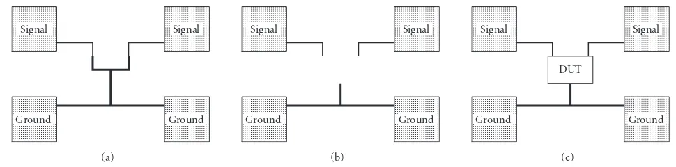
Several accumulation-mode varactor test structures are placed on a test chip. Other than varactors, a short structure and an open structure are also placed on the chip to facilitate the de-embedding procedure. For this experiment, two dif-ferent varactors are characterized. Both varactors are made up of multiples of a unit varactor cell: one has 100 multi-ples (m100 array) and the other has 60 multiples (m60 ar-ray). The unit varactor cell has a width of 7.9μm and a gate length of 0.13μm. To reduce the effect of distributed gate re-sistance, contacts are used on both sides of the polysilicon gates. Figure 12illustrates the three test structures: (a) the
short structure, (b) the open structure, and (c) the device under test (DUT), that is, varactor array.
Figure 13shows the micrograph of some of the test struc-tures on the die. These test strucstruc-tures from left to right are: short, open (including dummy varactors), and the varactor array (DUT).
3.3.1. De-embedding technique
Agilent 8510C vector network analyzer (VNA) is used for two-port RF characterization.S-parameters of the varactors, open, and short structures are measured from 100 MHz up to 6 GHz. The varactor voltage is varied from 1.5 V to 1.5 V, with 100 mV resolution.
Different de-embedding techniques are currently used. In [13], a three-step de-embedding technique is used that employs two short structures, an open structure and a thru-structure instead of only short and open thru-structures. A num-ber of de-embedding techniques have been discussed in [14]. We used two-step open/short de-embedding (OSD). Figure 14shows the equivalent circuit representation of the parasitic series impedance and shunt admittance of intercon-nects and contact pads, respectively.Z1andZ2are the inter-connection series impedances from pads to the varactor.Y1 andY2are the equivalent shunt admittances between the sig-nal and ground (pad capacitance, substrate capacitance, and resistance). We used signal-ground (SG or GS) probes. How-ever, GSG probes are preferred, as they result in balanced electrical characteristics.
Figure 15illustrates a different lumped model for OSD, as presented in [14]. HereZ
1andZ
2are the impedances be-tween the probe tips and the pads on the CMOS chip as the probe calibration is performed on an impedance-standard-substrate (ISS). The ISS uses gold metallization instead of typical aluminum traces, and has a lower resistance.
Both approaches to de-embedding shown in Figures14 and 15 were carefully considered. However, we concluded that in our setup, interconnection impedances are dominant. Based on the parasitic lumped model ofFigure 14,Y1andY2 are extracted from the following equations:
Y1=Y11,open,
Y2=Y22,open.
(6)
Z1andZ2can then be calculated using the following equa-tions: tances of the open and short structures, respectively.
3.3.2. Parameter extraction procedure
Signal Signal
Ground Ground
(a)
Signal Signal
Ground Ground
(b)
Signal Signal
Ground Ground
DUT
(c) Figure12: Top-view of the test structures: (a) short, (b) open, and (c) DUT (varactor array).
Figure 13: Micrograph of the test structures in 0.13μm CMOS, from left to right: short, open, and the varactor array (DUT).
capacitance associated with the series capacitance of the gate oxide and the depletion region under the gate.Cf models the fringing capacitance related to the sidewalls of the gate.Lg is the inductance of the poly gate.Rsis the poly gate and chan-nel resistance (the latter is voltage dependent), andRnwell is the resistance of then-well.Cdepis the depletion capacitance associated with the reversed biasedp-sub/n-well diode.Rsub andCsubare the substrate parasitics.Rsd is the resistance of then+ regions (bulk electrode).
In order to verify the model shown inFigure 16, we need to characterize the de-embedded on-chip varactors (m60 and m100 arrays). Figure 17shows the simplified form of Figure 16. In this figure, we have neglectedRsd (Zc), as the impedance of the highly dopedn+ regions is very small (less than 1Ωin these test structures).
Using the simplified circuit shown inFigure 17, we ex-tractZaandZbfrom the following two equations:
Za= 1
Y11 =Z11 Z 12,
Zb=Z12=Z21=Z22,
(8)
whereZ11,Z12,Z21, andZ22are the equivalentZ-parameters of the two-port varactor (Figure 17) andY11is the input ad-mittance (gate-side) of the equivalent Y-parameters.
Zacan be written as (neglectingCf):
Za=RS+ 1
jωCS +jωLg. (9)
Using (9) and employing numerical methods, we extracted the elements ofZafor both varactors (m60 andm100 arrays).
Rsis equal to real part ofZa(i.e., Re(Za)), andCsis calculated from
CS=
1 ω2L
g ωIm
Za
, (10)
whereLgis also calculated at higher frequencies (e.g., 6 GHz) using
Lg=
1 +ωCS-LowIm
Za
ω2C S-Low
, (11)
CS-Low is the capacitance at lower frequencies (e.g.,
100 MHz), whereω2L
g is insignificant and can be removed from (10).
The quality factor (Q) of the varactor, which is the ratio of the stored energy to the dissipated energy (resistive loss) in the varactor, can also be approximated by
Q=Im
Za
ReZa
. (12)
The substrate effect (Zb) is calculated using similar methods described forZa.
3.4. Varactor modeling
Ground pad
Ground pad DUT
(varactor)
Z1 Z2
S1
pad
S2
pad
Y1 Y2
Figure14: Equivalent lumped model of the varactor (DUT) with associated parasitics (open/short de-embedding).
DUT (varactor)
Z¼
1 Z
¼
2
Y¼
1 Y
¼
2
Ground Ground
S1 S2
Figure15: Alternative lumped model for open/short de-embedding (OSD).
Za
Zc
Rs Cs
Gate Lg Rsd Bulk
Cf
Rnwell
Cdep
Csub Rsub
Zb
Figure16: Equivalent lumped model of the integrated varactor.
Figure 16 illustrates the model of this varactor con-structed with passive circuit elements, and based on physical parameters [6]. As mentioned above, this model requires the implementation of nonstraightforward equations (e.g., hy-perbolic tangent) in the circuit-design environment and may involve other approximations as well. Moreover, the model cannot be easily scaled to future technologies.
Za
Zb
Gate Bulk
Sub Sub
Figure17: Simplified circuit of the two-port varactor inFigure 16.
We have considered a number of different equivalent models reported in the literature and developed a new model that closely approximates the measured characteristics of the VCO [15]. This improved model is shown inFigure 18, and is a modified version of that proposed in [8]. The overlap capacitanceCov, a voltage sourceVoffset, and a voltage source (dashed lines) between the bulk and drain/source have been added in the new model.
Voffset=1.1 V
Rg
Cav
Gate
Sidewall and area diode (n-well/p-sub)
RareaandRsidewall Sub
Bulk (n-well)
Ra
5 V +
+ C
junctionis scaled down (e.g., by 10 6)
or a negative power supply is used
Figure18: SPICE model developed for the varactor.
source/drain terminal is required to eliminate the inversion layer capacitance present in the channel of the pMOS but absent in the varactor structure (seeFigure 9). As a result, the gate to n-well (bulk) capacitance of pMOS represents the varactor capacitance properly with an additional chan-nel length correction for LDD (lightly doped source/drain) regions. Unfortunately in this configuration, the gate-source and gate-drain overlap components of the varactor get ne-glected; as a result, they have to be added back by using the fixed capacitor,CovVoffsetrepresents a difference of the
metal-semiconductor work functionφMS, as the pMOS has p+ poly gate doping while the varactor has n+ poly dop-ing due to their different source/drain diffusion. As doping levels in the polysilicon layer are typically close to degenera-tion, theVoffset is close to silicon bandgap (Eg(T)/q), which is about 1.1 V at room temperature. Finally, the junction ca-pacitance of the pMOS transistor has to be scaled down. This can be done either by changing the scaling factor inside the SPICE model or adding a negative power supply between source/drain and the bulk (e.g., 5 V) to enlarge the deple-tion area and reduce the juncdeple-tion capacitance.
4. EXPERIMENTAL RESULTS
Three different VCO structures have been fabricated in a standard 0.13μm CMOS process with a 1.2 V power sup-ply. No special mixed-signal process options have been used. The micrograph of the chip is shown inFigure 19. Varactors are implemented asn+ accumulation-mode MOS capacitors with no additional mask required. Thus, the obtained de-signs are portable to various CMOS processes of different foundries.
The three implementations have similar architectures as those depicted in Figures 7(b) and 7(c), but with diff er-ent varactor values. The tail currer-ent in all three versions is 1.5 mA; hence the DC power consumption is 1.8 mW, excluding output driver and biasing circuits. The one that
Figure19: Micrograph of a VCO test structure in 0.13μm CMOS.
105 106 107 108
130 120 110 100 90 80 70 60 50
Frequency
Phase
n
oise
(dBc)
Figure20: Measured phase noise of the VCO with pMOS tail cur-rent (Figure 7(b)) at three different supply voltages (1.2 V, and 1.2 V
5%).
incorporates an nMOS tail current source (Figure 7(c)) ex-hibits higher sensitivity to the power supply noise, while the one with a pMOS tail current source (Figure 7(b)) has the best power-supply-rejection ratio (PSRR), due to the extra isolation from the power supply by the current source.
In addition to the three VCO circuits, a biasing circuit and an output driver stage were added to drive external 50Ω load. Individual varactor and inductor test structures were also included for S-parameter measurements. Open and short de-embedding structures were added for proper extraction of the equivalent circuit, as explained earlier in Section 3.3.1.
The phase noise of all three VCOs was measured using a spectrum analyzer with a phase noise module.Figure 20 compares the phase noise of the VCO with the pMOS tail current shown in Figure 7(b), for three different sup-ply voltages (1.2 V, and 1.2 V 5%) at the nominal
0 0.2 0.4 0.6 0.8 1 1.2
Figure21: Measured versus modeled tuning characteristics (new SPICE model).
(600 mV). The phase noise at 1 MHz offset from the carrier is 95.8/ 95.5/ 95.5 dBc/Hz, respectively.
The tuning characteristics were simulated using the var-actor model described in Section 3.4. Excellent agreement between the model and the measurement was obtained, as shown inFigure 21. The results inFigure 21are for a VCO test structure with an increased number of varactor fingers (varactor with 100 fingers) and hence lower center frequency compared to the results shown inFigure 10.
5. CONCLUSION
VCOs are among the critical building blocks of wireless RF transceivers since their performance and phase noise po-tentially affects the overall transceiver performance. Among various VCO architectures, LC VCOs have superior phase noise performance and therefore are extensively used in RF transceivers. Varactors are the main tuning component of LC VCOs and play an important role in the phase noise per-formance and tuning capability of these types of VCOs. A new model for CMOS accumulation—mode varactors is pre-sented. The model is used to predict the tuning curve of the LC VCOs. The shape of the tuning curve and the effective varactor capacitance were shown to depend on the losses of the tank and the magnitude of the tail current. The model is SPICE-based and has been verified experimentally in a stan-dard 0.13μm CMOS process with different VCO structures.
ACKNOWLEDGMENTS
The authors would like to thank Roberto Rosales of the Uni-versity of British Columbia and Mark Hiebert of PMC-Sierra for assisting with the measurements. This research was sup-ported in part by Natural Sciences and Engineering Research Council of Canada (NSERC), PMC Sierra, CMC Microsys-tems, and Canadian Foundation for Innovation (CFI).
REFERENCES
[1] J. Craninckx, M. Steyaert, and H. Miyakawa, “A fully inte-grated spiral-LC CMOS VCO set with prescaler for GSM and DCS-1800 systems,” in Proceedings of the IEEE Custom In-tegrated Circuits Conference, pp. 403–406, Santa Clara, Calif, USA, May 1997.
[2] C. Samori, S. Levantino, and V. Boccuzzi, “A -94 dBc/Hz@100 kHz, fully-integrated, 5-GHz, CMOS VCO with 18% tuning range for Bluetooth applications,” inProceedings of IEEE Cus-tom Integrated Circuits Conference, pp. 201–204, San Diego, Calif, USA, May 2001.
[3] R. Walker, “Clock and Data Recovery for Serial Digital Com-munication,” ISSCC short Course, February, 2002.
[4] A. Hajimiri and T. H. Lee, “A general theory of phase noise in electrical oscillators,”IEEE Journal of Solid-State Circuits, vol. 33, no. 2, pp. 179–194, 1998.
[5] P. Andreani and S. Mattisson, “On the use of MOS varactors in RF VCOs,”IEEE Journal of Solid-State Circuits, vol. 35, no. 6, pp. 905–910, 2000.
[6] S.-S. Song and H. Shin, “An RF model of the accumulation-mode MOS varactor valid in both accumulation and depletion regions,”IEEE Transactions on Electron Devices, vol. 50, no. 9, pp. 1997–1999, 2003.
[7] A.-S. Porret, T. Melly, C. C. Enz, and E. A. Vittoz, “Design of high-Q varactors for low-power wireless applications using a standard CMOS process,”IEEE Journal of Solid-State Circuits, vol. 35, no. 3, pp. 337–345, 2000.
[8] K. Moln´ar, G. Rappitsch, Z. Huszka, and E. Seebacher, “MOS varactor modeling with a subcircuit utilizing the BSIM3v3 model,”IEEE Transactions on Electron Devices, vol. 49, no. 7, pp. 1206–1211, 2002.
[9] R. L. Bunch and S. Raman, “Large-signal analysis of MOS var-actors in C MOS -Gm LC VCOs,”IEEE Journal of Solid-State Circuits, vol. 38, no. 8, pp. 1325–1332, 2003.
[10] E. Hegazi and A. A. Abidi, “Varactor characteristics, oscillator tuning curves, and AM-FM conversion,”IEEE Journal of Solid-State Circuits, vol. 38, no. 6, pp. 1033–1039, 2003.
[11] S. Levantino, C. Samori, A. Bonfanti, S. L. J. Gierkink, A. L. Lacaita, and V. Boccuzzi, “Frequency dependence on bias cur-rent in 5-GHz CMOS VCOs: impact on tuning range and flicker noise upconversion,” IEEE Journal of Solid-State Cir-cuits, vol. 37, no. 8, pp. 1003–1011, 2002.
[12] A. Hajimiri and T. H. Lee, “Design issues in CMOS differen-tial LC oscillators,”IEEE Journal of Solid-State Circuits, vol. 34, no. 5, pp. 717–724, 1999.
[13] H. Cho and D. E. Burk, “A three-step method for the de-embedding of high-frequency S-parameter measurements,”
IEEE Transactions on Electron Devices, vol. 38, no. 6, pp. 1371– 1375, 1991.
[14] T. E. Kolding, “On-wafer calibration techniques for giga-hertz CMOS measurements,” in Proceedings of IEEE International Conference on Microelectronic Test Structures (ICMTS ’99), pp. 105–110, Goteborg, Sweden, March 1999.
Pedram Samenireceived his B.S. (honors) degree in electrical engineering from the University of Tehran, Iran, in 1999 and the M.A.S. degree in analog and mixed sig-nal design from Simon Fraser University, Canada, in 2002. He is currently pursuing his Ph.D. in analog and mixed signal de-sign in the System-on-Chip (SoC) Lab of the University of British Columbia, Vancou-ver, Canada. His research interests include
clock and data recovery circuits for high-speed telecommunication systems. During the summer of 2004 he was with PMC-Sierra, Van-couver, Canada, where he worked on MOS varactor modeling and LC VCO characterization in CMOS 0.13μm process. From August 2005 to March 2006 he was with Foveon, Inc., Santa Clara, USA where he worked on characterization and modeling of circuits and devices used in CMOS image censor circuits.
Chris Siureceived the B.S. degree in elec-trical engineering from Simon Fraser Uni-versity, Burnaby, Canada, in 1991, and the M.S.E.E. degree from Stanford University, California, in 1994. He has over 10 years of experience in RF/Analog IC design and management, having worked for companies in both Canada and the US including PMC-Sierra, Philips, and Hewlett Packard. He was a Ph.D. student at the University of Alberta,
Edmonton, Canada, involved in the research of RF transceiver cir-cuits.
Shahriar Mirabbasireceived the B.S. degree in electrical engineering from Sharif Uni-versity of Technology, Tehran, Iran, in 1990 and the M.A.S. and Ph.D. degrees in elec-trical and computer engineering from the University of Toronto, ON, Canada, in 1997 and 2002, respectively. During the summer of 1997, he was with Gennum Corpora-tion, Burlington, ON, Canada, working on the system design of cable equalizers for
se-rial digital video and HDTV applications. From January 2001 to June 2002, he was with Snowbush Microelectronics, Toronto, ON, Canada, where he worked on designing high-speed mixed-signal CMOS integrated circuits including ADC and serializer/deserializer blocks. Since August 2002, he has been an Assistant Professor in the Department of Electrical and Computer Engineering of the Uni-versity of British Columbia, Vancouver, BC, Canada. His current research interests include analog and mixed-signal integrated cir-cuits and systems design for wireless and wireline communication applications, biomedical implants, and sensor networks.
Hormoz Djahanshahi received the B.S. (honors) and M.S. (honors) degrees in elec-trical engineering from Tehran Polytechnic University, and the Ph.D. degree in elec-trical and computer engineering from the University of Windsor, Canada, in 1998. In 1990–1992, he was with Fajr Microelectron-ics and developed biomedical instrumen-tation for patient monitoring in intensive care units. While at VLSI Research Group
in Windsor, he worked on CMOS implementation of artificial neu-ral networks and smart photosensors. In 1998 and 1999, he was a postdoctoral fellow at the University of Toronto, Canada, and
designed high-speed I/O, oscillators, and PLLs in CMOS and HBT technologies. He received the Best Paper Award at 1999 Micronet Symposium, Ottawa. Since 2000, he has been with PMC-Sierra, Vancouver, Canada, where he is currently a Leader in Technology Development Group. His work includes specification and design of high-performance mixed-signal blocks for multi-Gigabit-per sec-ond wireline and wireless applications. He has designed to produc-tion numerous clock synthesizer, clock/data recovery and SerDes components in 0.18μm, 0.13μm, and 90 nm CMOS. He has over 30 publications, one US patent, and is a Chapter Officer with IEEE SSCS in Vancouver.
Marwa Hamourreceived her Bachelor’s of electrical and electronic engineering from the Imperial College of Science, Technology & Medicine in 2000. She received her Mas-ter’s of applied science from the University of British Columbia, Canada, and is cur-rently reading for her Ph.D. at the same uni-versity.
Krzysztof Iniewskiis an Associate Professor at the Electrical and Computer Engineering Department of the University of Alberta. He is also the President of CMOS Emerg-ing Technologies Inc., a consultEmerg-ing com-pany in Vancouver. His research interests are in advanced CMOS devices and circuits for ultralow power wireless systems, med-ical imaging, and optmed-ical networks. From 1995 to 2003, he was with PMC-Sierra and
held various technical and management positions in Research & Development and Strategic Marketing. Prior to joining PMC-Sierra, from 1990 to 1994 he was an Assistant Professor at the University of Toronto, Electrical Engineering and Computer Engi-neering Department. He has published over 80 research papers in international journals and conferences. He holds 18 international patents granted in USA, Canada, France, Germany, and Japan. He is a frequent invited speaker and consults for multiple organizations internationally. He received his Ph.D. degree in electronics (hon-ors) from the Warsaw University of Technology (Warsaw, Poland) in 1988. Together with Carl McCrosky and Dan Minoli, he is an au-thor ofData Networks—VLSI and Optical Fibre, Wiley, 2006. He is also an editor ofEmerging Wireless Technologies, CRC Press, 2006.
Jatinder Chana completed the Bachelor’s and Master’s degrees in electrical engineer-ing at University of Victoria, BC, Canada, in 1992 and 1994, respectively. He joined PMC-Sierra in 1995 and have since then de-signed and implemented delta-sigma A/D converter, pipeline A/D converter, digital filters, high-speed data and clock recovery circuits for 3.125 Gbs, 2.5 Gbs Serdes, and low-jitter CSUs for 4.25 GHz and 6.25 Ghz