Self-Powered IoT Node High Efficiency Solar
Power Management System
Mr R.Mohammedabdullah, Mr.T.Harish Babu, Mr S.Syed Abdul Haq, Mrs.K.Elavarasi,
Asst. Professor, Sethu Institute of Technology, Tamilnadu, India
ABSTRACT: An efficient micro-scale solar power management architecture for self-powered Internet-of-Things node is presented in this paper. The proposed architecture avoids the linear regulator and presents a complete on-chip switched capacitorbased power converter in order to achieve higher end-to-end efficiency. Unlike traditional architectures, where the harvested energy processes twice, the proposed architecture processes the harvested energy only once before it reaches to the load circuit, irrespective of the ambient conditions. The system efficiency has been improved by 12% over the traditional architecture. The entire power management system has been designed using 0.18-μm CMOS technology node, and the circuit simulations demonstrate that the proposed architectural changes bring in a system efficiency of 82.4% under different light conditions. In addition to that, a hardware setup is created using commercially available ICs and photovoltaic cells, to validate that the proposed power management system is practically realizable. Index Terms—DC-DC converter, energy processing, energy scavenging, Internet of Things (IoT), maximum power point tracking, photovoltaic cell, wireless sensor nodes
I.INTRODUCTION
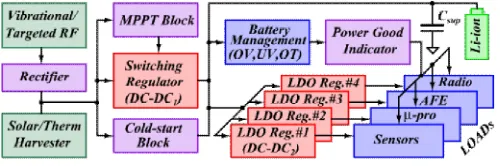
THERE is a great interest in powering IoT nodes by scavenging ambient energy, such as solar radiation [1], thermal gradient [2], mechanical vibration [3], or radio frequency (RF) waves [4]. Based on the applications and area of deployment, appropriate energy source/sources is/are utilized for powering the IoT node [5], [6]. As the ambient conditions are changing, one can not directly connect a harvester to the load as it is not regulated. Moreover, the available scavenged energy may not be sufficient for powering the sensor nodes all the time. Apart from that, unlike a battery, a harvester has a continuous source of power without depletion, but if it is not extracted continuously, the same would be unutilized and lost. Therefore, an interface circuit in between the load and the harvester is needed, in order to maintain regulation both at the input and the output.A typical power management architecture for IoT node is shown in Fig. 1.
Fig. 1. Typical power management architecture of an IoT node.
this architecture, as the energy is processed twice before it reaches the load circuits, the overall efficiency expected is
ηDC−DC,1×ηDC−DC,2 and its typical values lies between 65−75%. This includes power transfer losses of associated interface circuits [8], [9]. One of the key issues with this architecture is that the
overall efficiency varies with ambient condition. Because the first switched capacitor DC-DC converter has a fixed voltage up-conversion ratio and its output voltage varies with ambient condition. As a result, the drop across LDO varies with ambient condition and much of the extracted power may simply be dissipated within the LDO, and hence, the overall efficiency will degrade accordingly. Another key issue is that often it utilizes two DC-DC converters even if there is sufficient ambient energy to power the load circuit. In order to address these issues, an efficient architecture has been proposed with following silent features: 1) the overall efficiency
varies minimally with ambient condition, 2) unlike
Fig. 2. Proposed power management architecture and the associated control signals for maintaining regulation at the load. VPH represents the PV cell terminal voltage and fCLK represents the frequency of
the switching converter.
traditional architecture, input energy processes once before it reaches to the load circuit, and hence, overall efficiency has been improved by 12%, and 3) avoid inductive and linear converters, but presents a completely on-chip switched capacitor based architecture.
The rest of the paper is organized as follows: Section II discusses the proposed system architecture and its operation. Section III describes the circuit implementation of the proposed architecture. Section IV presents the hardware setup, measurement and simulation results to validate the proposed idea, and finally, Section V concludes the paper.
II.PROPOSED POWER MANAGEMENT ARCHITECTURE
from the sleep state to an active state if the input voltage is lower than the MOSFET threshold voltage. It will generate an auxiliary voltage higher than the MOSFET threshold voltage, which will eventually turn on the switches of the DC-DC1 converter and starts transferring charges from the harvester to the load circuit. Previous works report solutions for start-up issue [10], [11] and therefore, this implementation does not focus the startup issues but assumes that the supercapacitor, CB, is initially charged to bring up the system from the sleep state to an active state.
In order to maintain regulation at the load, VLis compared with the internal reference voltages VR1 and VR2, for gen- erating control signals, P1 and P2, and associated switching signals, S1, S2, S3 and S4, as shown in Fig. 2. Initially,
VL is less than VR1 and VR2, and the corresponding control signals are P1 = 1 and P2 = 1, and associated switching signals are S1 = 1, S2 = 1, S3 = 0 and S4 = 1, which will eventually activate the buffer stage as a converter mode and start delivering charges from buffer stage to the application stage to meet the charge deficiency. Once the load regulation is achieved during the negative half cycle of clock, and if the solar energy is more than enough to supply the load, then the corresponding control signals will be P1 = 0 and P2 = 0, and the associated switching signals will be S1 = 0, S2 = 1, S3 = 1 and S4 = 0, which will eventually enable the buffer stage as a storage mode for recharging the supercapacitor CB. On the contrary, during the positive half cycle, if there is insufficient ambient energy to supply the load, i.e., VL < VR2, control signals, P1 = 1 and P2 = 1, and associated switching signals, S1 = 1, S2 = 1, S3 = 0 and S4 = 1, will activate buffer stage as converter mode, in order to maintain regulation at the load. Therefore, due to the involvement of complementary switching between the buffer stage and the application stage, one could expect few tens of mV supply ripple along with the regulated power supply. The magnitude of this ripple depends on the op-amp offset voltage and the delay in the feedback loop. In comparison with the classic architecture shown in Fig. 1, the proposed architecture consists of single stage of DC-DC converter instead of two stages of DC-DC converter in between the harvester and the load. That means, the input energy is processed only once before it reaches to the load. Therefore, due to having two stages of DC-DC converters in series, the classic architecture will be limiting with respect to the overall efficiency compared to the proposed architecture. In addition to that, the proposed architecture avoids power inefficient linear regulators (i.e.,LDOs) and presents an efficient on-chip switched capacitor based architecture.
Generally, the conversion efficiency of a solar cell varies 10% − 40% and degrades further when the ambient light intensities are varying continuously. The conversion efficiency of a PV cell can be improved by tracking and offering optimal impedances dynamically and such a process is known as maximum power point tracking (MPPT). This paper adopted
a low-overhead adaptive MPPT scheme based on the negative feedback control loop [12], which eliminates power hungry micro-controller, current/voltage sensor, analog/digital comparator, and bulky capacitors and resistors. In order to adjust the input impedance of the switching converter for matching with harvester impedance, switching frequencies are varied from few MHz to tens of MHz. The frequency at which the maximum power transfer take place is known as maximum power point (MPP) frequency, fMPP. In order to track MPP adaptively with respect to the changes in ambient condition, inherent negative feedback control loop is utilized. This concept is illustrated in Fig. 2, the VPH vs.
fCLK plot.
There are two independent relationships between the same physical variables, fCLK and VPH, that arise from different sources: i) change in converter input impedance and hence VPH with fCLK (the red lines) under two different light conditions, and ii) the change in oscillation frequency fCLK with CS-VCO control voltage (the blue line). It is to be noted that, for a given light intensity there is only one intersection point (either A or B) between these two curves and the system will settle at that operating point. In other words, at zero switching frequency, there will be no charge transfer takes place through the switching converter and thus VPH will be the open circuit voltage, VOC. As the switching frequency increases, the charge transfer take place and VPH will begin to reduce the input impedance of the switching converter.
On the contrary, the oscillator frequency reduces as VPH starts decreasing. This brings the possibility of an equilibrium point (either point A or B), where both curves will intersect each other and the circuit will lock on that particular switching frequency.
transferring charges either to the load capacitor/supercapacitor. As the part of IPH, begins to flow through the switching converter,
Fig. 3. Simplified block diagram of the proposed architecture for understanding the inherent negative feedback loop for tracking maximum power points.
Fig. 4. (a) PV cell output power voltage characteristics, (b) System desired V-f characteristic, and (c) CS-VCO and system desired V-f characteristics.
charging current of CI N , i.e., IPH − II N , starts reducing and eventually becomes zero when IPH = II N . On this point, oscillator locks its frequency and remains in its state until
there is any alteration in ambient light intensities. Now, if there is a change in ambient light intensity, immediately the
IPH will goes either up or down, however, II N will not change imminently due to the delay involved in the feedback loop and therefore, the error current, IPH −II N , either goes up or down which eventually reflects on VPH. Once VPH
is changed, fclk will change the input impedance of the switching converter accordingly, which will change II N and reduces the error current and eventually becomes zero after few iteration.
Now, in order to make sure that the locking frequency is the maximum power point (MPP) frequency, CS-VCO has been trained in such a way that it passes through all the system desired MPP points as shown in Fig. 4. Fig. 4(a) shows the PV cell power voltage characteristics and maximum power points under different light intensities. To extract maximum power from this harvester, switching converter input voltage has to be the maximum power point (MPP) voltages, which are marked as a blue dots. In order to get these VMPPs, CS-VCO has been disconnected from the loop and plotted the combined characteristics of PV cell and switching converter in Fig. 4(b), which is nothing but system desired V − f characteristic.
Therefore, one has to design a CS-VCO, which will approximate the desired V − f curve well enough such that the disparity between them is negligible as shown in Fig. 4(c). Therefore, every stable point will be the MPP point of this feedback control loop.
III.CIRCUIT IMPLEMENTATION
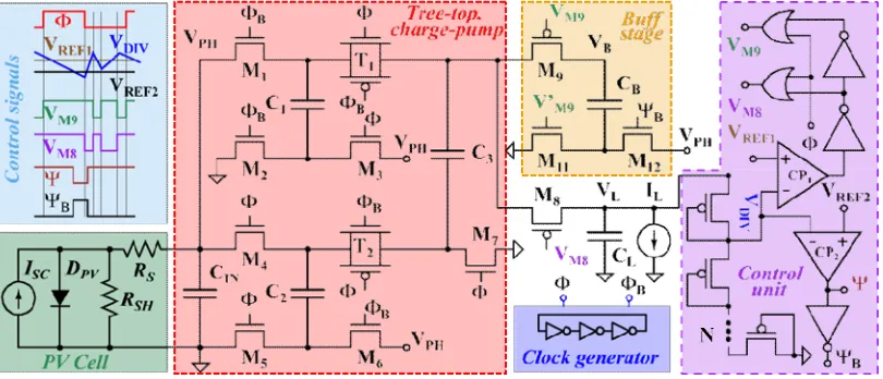
Fig. 5. Circuit diagram of the proposed power management architecture.
topology. To realize charge transfer switches (CTSs), n-MOS and p-MOS transistors and transmission gates are employed. Placement of respective CTSs are made based on their terminal voltages in order to get lower on resistance [14]. Pumping capacitors are realized by on-chip MOS gate capacitors to achieve compact chip area. Due to the presence of a switching converter in between the harvester and load, harvester voltage will experience some ripple, and one can suppress it by placing a capacitor, CI N , in between the harvester and switching converter. In control unit, in order to get a scaled version
of load voltage with low power consumption and small area, a voltage divider is formed by cascading PMOS transistors in subthreshold regime instead of a traditional resistor divider circuit. Two analog comparators are used to compare the scaled load voltage, VDIV , with two reference voltages, VREF1 and VREF2. A two-stage open loop transconductance amplifier with push-pull inverters in a cascade is used to realize the comparator circuit, as described by Allen and Holberg [15]. However, special care has been taken into consideration to realize high speed (> 50 MHz) as well as low voltage (VDD = 1 V) operations. CMOS inverters and logic gates are used
Fig. 6. Non-overlapping clock generator circuit.
VM8 or VM9 during the negative half cycle of , and their corresponding timing diagrams are shown in Fig. 5. Depending on comparator triggering, switching converter will connect either buffer stage or application stage. If
VDIVis lower than VREF1 during the negative half cycle of , VM8 will trigger the M8 transistor and VM9 will turn off both M9 and M11 transistors, in order to maintain load regulation. Once the input energy meets the supply requirements, i.e., VDIV > VREF1, M8 will be turn off and M9,11 will be turned on for storing the excess energy. Therefore, due to complementary switching between application stage and buffer stage, VLis regulated and the remaining excess energy, is stored in the storage capacitor CB, for future uses. Now, if VDIVis even lower than VRE F2, that means, the scavenging energy is not sufficient to meet the load requirements, a control signal will trigger the M12 transistor, which will then allow the discharge of CBto the CL in order to mitigate any imbalances between available input energy and the output energy. In order to validate this idea, a system level simulation is carried out and a hardware setup
Fig. 9. Output power variation with respect to PV cell terminal voltage for three different light conditions.
is created using commercially available ICs, capacitors, and solar mini-panels and they are described in the next section.
IV. MEASUREMENT AND SIMULATION RESULTS
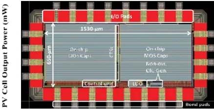
The proposed power management interface circuit is designed and simulated in 0.18-μm CMOS technology and its layout is shown in Fig. 7. The layout dimensions of the interface circuit is 1530 − μm×650 − μm and the major area of occupation is mainly due to the pumping capacitors. Post-layout simulations are carried out using standard foundry MOSFET models. The sizes of the power transistors (W/L) and pumping capacitors are chosen as 600μm/0.18μm and
500 pF, respectively. In order to suppress the input ripples, CINis chosen as 12 nF and to reduce the simulation time,
buffer capacitor CBand load capacitor CLare chosen as 30 nF and 10 nF, respectively.
A.Photovoltaic Harvester
To emulate the PV cell in the simulation engine, an elec- trical equivalent model is used as an input energy source as shown in Fig. 5. To find the model parameters of this equivalent circuit, an experiment was conducted with two series-connected PV cells (Model 1-100, from Solar World Inc. [17]). A 40-Watt bulb is used as the light source and to emulate ambient variations, the position of the light bulb with respect the harvester is varied. In order to vary the load resistance, a standard potentiometer with the range of 0 − 10 K is used. Fig. 8 and 9 shows the output current and
Fig. 10. Simulated waveform of clk and clkb under 405 mV control voltage and 1.5 V supply voltage. Fig. 8. Output current variation with respect
power variation with respect to PV cell terminal voltage for three different light conditions, 500 lx, 1000 lx, and 1500 lx, respectively. It may be noted that for a given light intensity, the output of solar cell behaves like a current source combined with a voltage limiter and at the transition point (where area under the curve is maximum), it offers maximum output power shown in Fig. 9. Now, from the slope of measured I − V
characteristic (dotted lines), one can calculate the equivalent series (RS) and shunt (RSH ) resistances for the equivalent electrical model of a PV cell. The slope near to the open circuit voltage corresponds to the series resistance and the slope near to the short circuit current corresponds to shunt resistance. After fitting these parameters with appropriate short-circuit current, ISC, and a number of diodes in the electrical model, simulation is carried out and the results are plotted in Fig. 8 and 9 (solid lines). There is a mismatch in the open circuit voltage at 1500 lx, but for an energy processing circuit, matching is important at the transition point, where the PV cell offers maximum power to the interface circuit.
B.Non-Overlapping Clock Generator
An array of five-stage (M = 5) current starved invert- ers (CS-INV) and two phase shifters are used to achieve the
Fig. 11. Control signals variation with respect to ambient conditions. Left hand side represents enough ambient energy whereas right hand side represent insufficient ambient energy conditions [11].
desired clock frequencies for maximum power point. Voltages VL and VI N are used for power supply and for controlling the oscillation frequency, respectively. The (W/L) of PD1 and NB1 are kept at (0.36/0.18) μm and (W/L) of
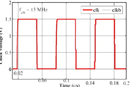
PO1 – POM and NO1 − NOM are kept at (1.80/0.18) μm and (0.90/0.18) μm, respectively. The (W/L) of PMOS and NMOS of CSINVs (I NV1−I NVM) are kept at (0.90/0.18) μm and (W/L) of PP1 − PPM and NP1 − NPM are kept at (0.72/0.18) μm and (0.36/0.18) μm, respectively, for this implementation. A reduced load clock load static master-slave register is used to realize D − FF [18]. To drive heavy loads, an array of progressively sized inverters are incorporated after the D− FF and their sizes are given in the figure itself, where, W represent the width of combined power transistors which are driven by the clock generator and e represents each stage efforts. A detailed discussion of progressive sizing inverters can be found in [16] and [19]. Fig. 10 shows the simulated waveform of the non-overlapping clock generator under supply voltage 1.5 V and control voltage 405 mV. The oscillation frequency achieved with this input condition is 15 MHz, with a cost of 12.3 μW power consumption.
1 C. Control Unit
turn on M9 and M10 transistors, and VM8 control signal will turn off M8 transistor. On the other hand, if the voltage
VDIV is lower than the reference voltage VREF1, control signal VM8 will turn on M8 transistor and turn off M9 and
M10 transistors, respectively, to maintain the regulation. However, if the voltage
Fig. 12. Complete system simulation when there is enough ambient energy to supply the load.
VDIV is even lower than the second reference voltage VREF2, then the control signal will turn-on M11 and M9 transistors by the control signal _, to transfer the charges from CB to CL . Therefore, an appropriate triggering of the control signals are occurred to provide better load
regulation.
D.Complete System Simulation
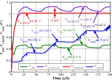
After integrating all the individual components of energy processing circuit, a system level simulation is carried out to quantify its benefits. First, we have simulated the complete system under enough ambient energy and afterward have examined the behavior when there is insufficient ambient energy for a small period of time.
1) Under Enough Ambient Energy: In such a light condition, the system will utilize only a single DC-DC converter
to maintain regulation at the load and the excess energy will be preserved in a storage capacitor CB. To emulate such varying light irradiance, the photocurrent, ISC, is varied fromemulate such varying light irradiance, the photocurrent, ISC , is varied from
2.70 mA to 3.50 mA which corresponds light intensity 600 lx to 1000 lx, and corresponding variations of PV cell terminal voltage, energy storage voltage, and load voltage are presented
Fig. 15. Conventional capacitor less low-dropout (CL-LDO) regulator.
Fig. 14. System efficiency as a function of photovoltaic cell voltage for the proposed and traditional architecture.
in Fig. 12. For PV cell terminal voltages, (VPH), 415 mV and 465 mV, the unregulated load voltages (VLOAD,UR) reached are 1.04 V and 1.130 V, and regulated load voltage (VLOAD,R)
reached is 1.01 V, respectively. It took less than 20 μs to reach its steady state value for each light irradiance step. The proposed architecture will work properly once the photocurrent reached is above or equal to 2.70 mA, otherwise, the load voltage will goes below 1 V, and one may not be able to maintain the desired regulation at the load. Therefore, during this light condition, there will not be any excess energy that
can be stored in a rechargeable battery. On the contrary, when the photocurrent reaches 3.50 mA, which is more than enough to supply the load, and the excess energy will be stored in a storage unit for further use, as shown in Fig. 12.
2) Under Insufficient Ambient Energy: In this light condition, the proposed system will utilize the stored energy
to maintain the load regulation. The variation of PV cell terminal voltage, energy storage voltage, and the regulated and unregulated load voltages are presented in Fig. 13. For PV cell terminal voltages 330 mV to 405 mV, the unregulated load voltage varies between 1.132 V to 0.922 V. Therefore, to maintain regulation at the load, one has to store the excess energy when VPH is 405 mV and utilize this energy when VPH is 330 mV. By doing so, one can achieve a regulated load
generator.
Fig. 17. Measurement results of PV cell terminal voltage (VPH ), non-overlapping clock signals (CLK and CLK_B), and no-load output voltage (VLO AD) at 100 lx light intensity.
Fig. 18. Transient response when the light intensities varies from 100 lx to 330 lx: (a) initial stage, when the light intensity change from 100 lx to 330 lx, (b) after 21 sec, while maintained light intensity 330 lx, (c) after 44 sec,
In order to calculate the effective system efficiency, one has to consider the power transfer loss due to both the control unit and the non-overlapping clock generator [22]. The power consumed by the clock generator at a supply voltage 1.5 V
is 12.3 μW, whereas, the control unit consume 18.3 μW at 15 MHz clock frequency. Therefore, while calculating the net harvested power, one has to deduct these power from the output power. Fig. 14 shows the overall system efficiency as a function of PV cell terminal voltage of the proposed and traditional architecture. In order to calculate the overall system efficiency, average input power and average output power are taken into consideration as the ambient condition are changing with time [12]. Once the interface circuit provides regulation at the load, the overall efficiency of the system is calculated. The proposed architecture achieved a peak efficiency of 82.4% for input voltages higher than 365 mV. In order to compare with traditional power management architecture, a capacitor-less low-dropout regulator (CL-LDR) [23] has been incorporated (as shown in Fig. 15) in between the switching regulator and the load, and the buffer stage is eliminated from the architecture. The error amplifier (EA) is designed to achieve a voltage gain 40 dB and the W/L of the pass transistor (MP) is kept at (2000/1)μm to deliver a load of 1.01 mW with the supply voltage (VI N) of 1 V. The open loop AC response shows a voltage gain of 59.22 dB and a phase margin of 84°. The overall efficiency achieved after incorporating the CL-LDR is 69.7% as shown in Fig. 14, where, ηDC−DC,1 (switching regulator), ηDC−DC,2 (CL-LDR), and VLOAD,URare 84%, 83.3%, and 1.01 V, respectively. As one move towards higher input voltage, the intermediate voltage (VLOAD,UR) goes up and reaches 1.132 V for VPH= 450 mV, and eventually the CL-LDR and overall system efficiency have degraded to 73% and 60%, respectively. Therefore, in comparison with proposed archi- tecture, the system efficiency has been improved by 12.7% for
VLOAD,UR= 1.01 V and 22.4% for VLO AD,UR = 1.132 V. Though the percentage of improvement depends on the
ambient light intensities, one can expect at least 12% improvement for this implementation.
E.Experiment Results
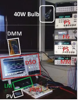
In order to validate the proposed power management scheme, a hardware setup is created using commercially avail- able ICs, capacitors, and solar mini-panels as shown in Fig. 16. ICs ALD1103 [24], LM2903P [25], and HEF4071B [26] are used for MOSFETs, comparators, and OR gates, respectively. Three 1 μF capacitors and two 1000 μF capacitors are used for
TABLE I
PERFORMANCE COMPARISON AMONG STATE-OF-THE-ART POWER MANAGEMENT ARCHITECTURE FOR
Fig. 19. Measurement of control signals at 330 lx light intensity.
charge transfer and storage, respectively. Two series connected mini solar panels (Model 1-100, from Solar World Inc. [17]) are used to convert light energy to electrical energy. A digital lux meter (Mastech MS6610 [27]) is used to measure the light intensity. For system clock, Agilent-33250A function genera- tor [28] is used and to generate non-overlapping clock signals phase shifter circuits are implemented using ALD1103 ICs. To represent ambient light energy, 40W light bulb is used for conducting the experiment. In order to vary the light intensity, the distance between the light bulb and solar panels are varied.
Fig. 17 shows the measurement results of PV cell termi-nal voltage (VPH), non-overlapping clock signals (CLK and CLK_B), and no-load output voltage (VLOAD) at 100 lx light intensity. Under this light intensity, VPHoffers 310 mV to the interface circuit and with the help of non-overlapping clock signals, the load voltage reached is 990 mV with ±
20 mV ripple. Once the load is connected (IL 100μA), under this light intensity, VLOAD is settled down to zero because of the insufficient light intensity for powering the load. Fig. 18 captures four images when the light intensity varies back and forth between 100 and 330 lxes. Fig 18(a) shows the initial stage waveforms where the light intensity changes from 100 lx to 330 lx. As soon as the light intensity increases, VPHreaches
375 mV and the load voltage starts increasing from the 0 V.
Once the load voltage reaches 1 V, buffer voltage VST O starts increasing as shown in Fig 18(b). The PV cell terminal voltage is increasing once the load voltage and buffer voltage approaches the final value as shown in Fig. 18(b) and (c). Because, initially the load capacitor was empty and the charge pump draws more current from the harvester, which eventually lowers the PV cell terminal voltage. Once the capacitor is charged, the load demand is reduced and eventually PV cell terminal current is reduced and the voltage is increased. After storing sufficient energy in the CB, light intensity was changed from 330 lx to less than 100 lx. Under such a condition, VPHhas come down to 210 mV, which is not enough to maintain regulation at the load. In such a condition, the stored energy is utilized and the regulation is maintained at the load as shown in Fig. 18(d). Therefore, it is apparent from the measurement results that the proposed technique can maintain regulation at the load, irrespective of whether there is enough or not enough ambient energies to supply the load.
ambient energy is insufficient to supply the load and to maintain regulation it utilizes the stored energy.
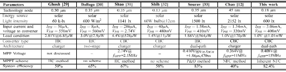
Table I shows the performance comparison among the state-of-the-art power management architectures for micro-scale
Fig. 20. Measurement of control signals at 100 lx light intensity.
solar energy harvesting systems. Among the capacitive boost converter, the proposed one has higher conversion efficiency and higher power delivery capability. Moreover, the proposed one has highest switching frequency which allows smaller component size and compact chip-area. Further, the proposed one has lower MPPT overhead as it utilizes inherent negative feedback loop for maximum power point tracking.
V. CONCLUSION
An efficient on-chip power management architecture for solar energy harvesting system is presented, which utilizes a single stage DC-DC converter when there is enough ambient energy for maintaining regulation at both the input and load. The proposed architecture utilized the stored energy to main- tain regulation when there is insufficient ambient energy to supply the load requirement. The proposed architecture avoids linear regulator and utilizes simple charge pump concept in order to maintain regulation. By utilizing a switching converter instead of a linear regulator, the proposed scheme achieved higher end-to-end efficiency. Simulation, as well as experi- mental result, are reported to validate the proposed idea.
ACKNOWLEDGMENTS
The authors would like to thank M. M. Vinaya and J. Sylvester for technical discussion.
REFERENCES
[1] F. Simjee and P. H. Chou, “Everlast: Long-life, supercapacitor-operated wireless sensor node,” in Proc. IEEE Int. Symp. Low Power
Electron. Design, Oct. 2006, pp. 197–202.
[2] A. Prijic´, L. Vracˇar, D. Vucˇkovic´, D. Milic´, and Z. Prijic´, “Thermal
energy harvesting wireless sensor node in aluminum core PCB technol- ogy,” IEEE Sensors J., vol. 15, no. 1, pp. 337–345, Jan. 2015. [3] L. Larcher et al., “Vibrational energy harvesting,” in Beyond-CMOS Nanodevices, vol. 1. Hoboken, NJ, USA: Wiley, 2014, pp. 89–134.
[4] P. Nintanavongsa et al., “Design optimization and implementation for
RF energy harvesting circuits,” IEEE J. Emerg. Sel. Topics Circuits Syst., vol. 2, no. 1, pp. 24–33, Mar. 2012. [5] C. Park and P. H. Chou, “AmbiMax: Autonomous energy harvesting
[6] C. Vankecke et al., “Multisource and battery-free energy harvesting architecture for aeronautics applications,” IEEE Trans. Power Electron., vol. 30, no. 6, pp. 3215–3227, Jun. 2015.
[7] Y. K. Ramadass, A. A. Fayed, and A. P. Chandrakasan, “A fully- integrated switched-capacitor step-down DC-DC converter with digital capacitance modulation in 45 nm CMOS,” IEEE J. Solid-State Circuits, vol. 45, no. 12, pp. 2557–2565, Dec. 2010.
[8] E. J. Carlson, K. Strunz, and B. P. Otis, “A 20 mV input boost converter with efficient digital control for thermoelectric energy harvesting,”
IEEE
J. Solid-State Circuits, vol. 45, no. 4, pp. 741–750, Apr. 2010.
[9] Y. K. Ramadass and A. P. Chandrakasan, “A battery-less thermoelectric energy harvesting interface circuit with 35 mV startup voltage,” IEEE
J. Solid-State Circuits, vol. 46, no. 1, pp. 333–341, Jan. 2011.
[10] H. Peng, N. Tang, Y. Yang, and D. Heo, “CMOS startup charge pump with body bias and backward control for energy harvesting step-up converters,” IEEE Trans. Circuits Syst. I, Reg. Papers, vol. 61, no. 6, pp. 1618–1628, Jun. 2014.
[11] S. Mondal and R. P. Paily, “An efficient on chip power management
architecture for solar energy harvesting systems,” in Proc. 29th Int. Conf. VLSI Design, Jan. 2016, pp. 224–229. [12] C. Lu, S. P. Park, V. Raghunathan, and K. Roy, “Low- overhead
maximum power point tracking for micro-scale solar energy har- vesting systems,” in Proc. 25th Int. Conf. VLSI Design, Jan. 2012, pp. 215–220.
[13] C. Lu, S. P. Park, V. Raghunathan, and K. Roy, “Efficient power conversion for ultra low voltage micro scale energy transducers,” in
Proc. Eur. Conf. Design, Autom. Test (DATE), 2010, pp. 1602–1607.
[14] W. M. C. Sansen, Analog Design Essentials, vol. 859. Springer, 2007.
[15] P. E. Allen and D. R. Holberg, CMOS Analog Circuit Design. London, U.K.: Oxford Univ. Press, 2013.
[16] N. Weste and D. Harris, CMOS VLSI Design: A Circuits and Systems
Perspective. Reading, MA, USA: Addison-Wesley, 2010.
[17] Solar Made Inc. Mini-Panel 0.5 V, 100 mA 1-100, accessed on Jun. 4. 2017. [Online]. Available: http://www.solarmade.com
[18] M. R. Jan, C. Anantha, and N. Borivoje, Digital Integrated Circuits—A Design Perspective. Prentice Hall, 2003.
[19] S. Mondal and R. Paily, “An efficient on-chip switched-capacitor-based power converter for a microscale energy transducer,”
IEEE Trans. Circuits Syst. II, Exp. Briefs, vol. 63, no. 3, pp. 254–258, Mar. 2016.
[20] S. Mandal, S. Arfin, and R. Sarpeshkar, “Fast startup CMOS current references,” in Proc. ISCAS, May 2006, p. 4.
[21] S. Mondal and R. P. Paily, “An efficient on-chip energy processing circuit
for micro-scale energy harvesting systems,” in Proc. 19th Int. Symp. VLSI Design Test (VDAT), Jun. 2015, pp. 1–5. [22] Y. K. Ramadass, “Energy processing circuits for low-power applica-
tions,” Ph.D. dissertation, Massachusetts Inst. Technol., Cambridge, MA, USA, 2009. [23] J. Torres et al., “Low drop-out voltage regulators: Capacitor-less archi-
tecture comparison,” IEEE Circuits Syst. Mag., vol. 14, no. 2, pp. 6–26, May 2014. [24] Advanced Linear Devices, Inc. [Online]. Available: http://www.aldinc. com/
[25] Dual Differential Comparators. Texas Instruments, accessed on May 4, 2017. [Online]. Available: http://www.ti.com/
[26] NXP Semiconductors. Quad 2-Input OR Gate, accessed on May 4, 2017. [Online]. Available: http://www.nxp.com/
[27] Mastech Digital Luxmeter MS, accessed on May 4, 2017. [Online]. Available: http://www.mastech.com/
[28] Agilent Technologies. Agilent Function/Arbitrary Waveform Gener-
ator, accessed on May 4, 2017. [Online]. Available: http://www. agilent.com/ [29] S. Ghosh, H.-T. Wang, and W. D. Leon-Salas, “A circuit for energy
harvesting using on-chip solar cells,” IEEE Trans. Power Electron., vol. 29, no. 9, pp. 4658–4671, Sep. 2014. [30] E. Dallago, A. L. Barnabei, A. Liberale, P. Malcovati, and G. Venchi,
“An interface circuit for low-voltage low-current energy harvesting systems,” IEEE Trans. Power Electron., vol. 30, no. 3, pp. 1411– 1420, Mar. 2015.
[31] H. Shao, C.-Y. Tsui, and W.-H. Ki, “The design of a micro power management system for applications using photovoltaic cells with the maximum output power control,” IEEE Trans. Very Large Scale Integr. (VLSI) Syst., vol. 17, no. 8, pp. 1138– 1142, Aug. 2009.
[32] Y.-C. Shih and B. P. Otis, “An inductorless DC–DC converter for energy harvesting with a 1.2-μw bandgap-referenced output controller,”
IEEETrans. Circuits Syst. II, Exp. Briefs, vol. 58, no. 12, pp. 832–836, Dec. 2011.
[33] S. Bandyopadhyay and A. P. Chandrakasan, “Platform architecture for
solar, thermal, and vibration energy combining with MPPT and single inductor,” IEEE J. Solid-State Circuits, vol. 47, no. 9, pp.
![Fig. 11. Control signals variation with respect to ambient conditions. Left hand side represents enough ambient energy whereas right hand side represent insufficient ambient energy conditions [11]](https://thumb-us.123doks.com/thumbv2/123dok_us/7761601.1274363/8.595.73.528.376.517/control-variation-conditions-represents-ambient-represent-insufficient-conditions.webp)