Highly Efficient Free Space Laser
Communication
Gibin Mathew Padayattil
1, Dixon Poly
2, Preejo K. Paulson
3, Miranda Thomas
4, Jitha Joseph
5B.Tech Student, Dept. of EEE, Sahrdaya College of Engineering & Technology, Kodakara, Kerala, India 1,2,3,4
Assistant Professor, Dept. of EEE, Sahrdaya College of Engineering& Technology, Kodakara, Kerala, India 5
ABSTRACT:This paper tells about the microcontroller based communication system using laser light as a device to transmit data. Here the microcontroller is connected with a PC where the PC act has an input to the laser which gives input parameters like audio, text and video to transmit with the help of laser medium. After successfully implementing this project, we found that the data transmission through laser light has achieved great success while comparing with the conventional communication system.
KEYWORDS:Laser, Solar Panel, Driver IC, Free Space Optics, Telecommunication.
I.INTRODUCTION
Our paper is based on the concept of laser (Light Amplification by Stimulated Emission of Radiation) for transmitting analog as well as digital signals. We have used phototransistor to receive the signal at receiver.
For voice transmission amplitude modulation of laser pulse was used to transmit the voice signal. Condenser microphone converts the voice into electric pulse which was then amplified and transmitted through laser. Photo detector at receiver detects the laser light and voice was output through loud speaker.
Data transmission is based on pulse width modulation by the use of microcontroller. Different width of laser pulse was used for different number and character. The second microcontroller was used to decode the different signal and the received data was given to the output.
II.LITEARTURE SURVEY
The Aim of this project is to design a communication system through Laser, a laser diode at the transmitting end act as a transducer to convert the digital data into laser form and transmitted, at the receiving end a laser transistor convert the laser data into digital form. Here the motive of using Laser is that while the transmitter and receiver must require line-of-sight conditions, they have the benefit of eliminating the need for broadcast rights and buried cables. Laser communications systems can be easily deployed since they are inexpensive, small, low power and do not require any radio interference studies.
III.PRINCIPLE OF OPERATION
Every atom has a certain energy levels, which may be high or low. Once excited by heating, it goes to high energy level. After certain time in high energy level, it return back to original energy level, consequently emitting energy in the form of light having energy E=hf. Incident photon with energy to E2-E1 interacts with an atom in conduction band, causing it toreturn to low energy level with the emission of second photon. This photon has same phase, frequency and polarization as first. This whole phenomenon is known as stimulated emission, which gives the laser its spectral properties such as narrow spectral width, highly directed beam and intense light.
A.Optical Detection Principles
When device is reverse biased then the electric field developed across the p-n junction sweeps mobile carriers (holes and electron) to their respective majority sides (p and n type material). The depletion layer is therefore created oneither side of the junction. This barrier has the effect of stopping the majority carriers crossing the junction in the opposite direction to the field. However, the field accelerates minority carriers from both sides to the opposite side of the junction forming the reverse leakage current of the diode. Thus intrinsic conditions are created in the depletion region.
A photon incident in or near the depletion region of this device which has an energy greater than or the equal to the band gap energy Eg (i.e. hf ≥ Eg) will excite an electron from the valence band to the conduction band. This process leaves an empty hole in the valence band and is known as the photo generation of an electron-hole (carrier) pair. Carrier pairs so generated near the junction are separated and swept under the influence of electric field to produce displacement by current in the external circuit in excess of any reverse leakage current. The depletion layer must be sufficiently thick to allow a large fraction of the incident light to be absorbed in order to achieve maximum carrier-pair generation. [4]
B.Pulse Width Modulation
In pulse width modulation the average value of voltage (and current) is controlled by turning the switch between supply and load on and off at a fast pace. The longer the switch is on compared to the periods, the higher the power supplied to the load will be. Duty cycle is expressed in percent, 100% being fully on. The advantage of using the PWM is that power loss, the product of voltage and current, of the switching device is close to zero. When it is in switch off condition then there is practically no current and when it is on there will be almost no voltage drop across the switch. Because of their duty cycle, on/off nature, they can use in digital controls too. [3]
C.
Amplitude ModulationAmplitude modulation (AM) is defined as a process in which the amplitude of the carrier wave is varied linearly with the message signal [3]. It is a technique used in electronic communication, most commonly for transmitting information via a radio carrier wave.The envelope of the amplitude modulated signal embeds the information bearing signal. The total power of the transmitted signal varies with the modulating signal whereas the carrier power remains constant. The main defect of this modulation is that in an AM wave the signal is in the amplitude variations of the carrier, practically all the natural and man noises consists of electrical amplitude disturbances. As a receiver cannot distinguish between amplitude that represents noise and that contain the desired signal so reception is generally noisy.
D. Serial Communication
Serial communication uses a single data line instead of the 8-bit data line of parallel communication. This helps to minimize the problem of transmission of data faced in 8-bit data communication. 8-bit data transmission works only if the cable is not too long, since long cable diminishes and distorts the signal. Also an 8-bit data path is expensive. Serial data communication uses either synchronous or asynchronous method for the transmission of the data.
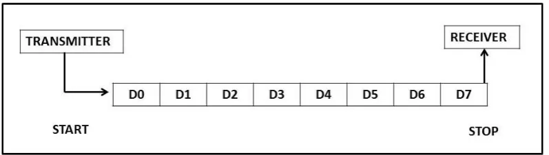
E. Asynchronous data communication
In this communication, transmitter and receiver are not synchronized. Each data character has a bit which identifies its start and 1 or 2 bits, which identify its end (framing). Sinceeach character is individually identified, characters can be sent at any time (asynchronously). When no data is being sent, the signal line is in a constant high or masking state. Following the data bit is a parity bit, which is used to check for errors in received data. Some system does not insert parity bit.
There are special IC chips for serial data communication, which are commonly known as the UART (universal asynchronous receiver-transmitter) and USART (universal synchronous-asynchronous receiver-transmitter). UART is basically the chips, a piece of hardware that translates data between parallel and serial forms. UART is the communication protocol to define the data formats need to be maintained to transmit the data.
Fig. 1 Asynchronous Data Format
In the fig 1, it shows the streaming of data format which often carries an MPEG Transport stream. It can carry one or multiple SD, HD or audio programs that are compressed.
F. Baud Rate
The baud rate of a data communications system is the number of symbol per second transferred. A symbol may have more than two states, so it may represent more than one binary bit (a binary bit always represents exactly two states). Therefore the baud rate may not equal the bit rate, especially in the case of recent modems, which can have (for example) up to nine bits per symbol. Microcontroller transfer and receive data serially at many different baud rates.
Fig. 2 Baud Rate
In the fig 2, it shows the measure of the number of data bits transmitted in one second. A figure of 2400 bits per second means 2400 zeros or ones can be transmitted in one second.
IV.HOW TRANSMISSION POSSIBLE THROUGH LASER
A. DTMF (Dual Tone Multiple Frequency) Technology
Each symbol is represented by the sum of the two frequencies that intersect the digit, the row frequencies are in a low band, below 1 kHz, and the column frequencies are in a high band, between 1 kHz and 2 kHz. The digits are displayed as they would appear on a telephone’s 4x4 matrix keypad (on standard telephone sets, the fourth column is omitted). The user should note that there are a number of different algorithms possible for generation and detection of DTMF tones; this application note simply describes one manner of doing so.
B. Decoding
Decoding a DTMF signal involves extracting the two tones in the signal and determining from their value the intended DTMF digit. Tone detection is often done in analog circuits by detecting and counting zero-crossings of the input signal. In digit circuits, tone detection is easier to accomplish by mathematically transforming the input time-domain signal into its frequency-domain equivalent by means of the Fourier transform, or through use of tone-specific digital filters. The general approach taken by this algorithm for DTMF tone detection is to take the Fourier transform of the observed signal and search for energy at the frequencies of interest.
coefficient of a DFT, is chosen over a fast Fourier transform (FFT) algorithm. There are two reasons for this In order to obtain the required frequency resolution at an 8 kHz sampling rate, a 256-point FFT would be required. Since the algorithm for tone detection requires knowledge of the energy at only 16 frequencies, it is more efficient to execute the Goertzel algorithm for these frequencies. In addition, the Goertzel algorithm is recursive, eliminating the need to store 256 samples for the FFT for each DTMF detector. This saves both time and data memory in the simulation and the real time applications.
V. DEMONSTRATION OF DATA TRANSMITTIER
There are 3 different modules of the project: A. Data Communication
B. Voice communication C. Optical Switching
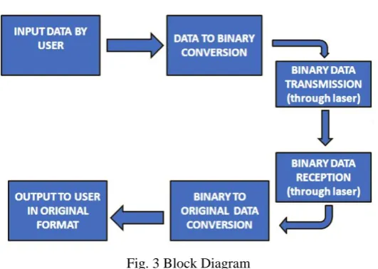
Fig. 3 Block Diagram
In the fig 3, it shows the block diagram of the entire circuit which consist of transmitting section, receiving section and the transferring channel.
A. Data Communication
The data communication through an optical fiber consists of a switch panel, when the user presses any particular switch (for example :- switch no 5) then the DTMF encoder IC UM 91214 will generate a unique pair of frequencies which will be passed to the optical source as the input and accordingly the signals of different frequencies for different keys, from the transmitter is passed through the fiber . This code sequence will be fed to an LED which will emit the light according to the sequence generated i.e. it will turn on for logic 1 and turn off for logic 0.
Then this light signal is transmitted to the receiver side, where it is reproduced as an electrical signal through a phototransistor or photodiode.
On the receiver side the received signals of different frequencies from the optical sensor is passed to the DTMF decoder IC 8870 which will convert it to BCD signal. These BCD signals are passed to the seven segment driver IC 7447 which will drive the seven segment display.
signal is transmitted to the receiver side, where it is given to seven segment display after decoding from the IC 8870 and then passing through IC 7447, which will then show 5 as its output.
B. Voice Communication
In the process of voice communication through an optical fiber, on the transmitter side, we use voice as the input signal. This signal is converted to an electrical signal through a condenser MIC. This electrical signal is processed by a modulator circuit and fed to an optical source which is an laser LED .The light signal from the LED varies according to the intensity of the voice signal .The more louder you speak, the glow of the LED will be more. Then the light signal is transmitted over an optical fiber to the receiver side. At this end a photo transistor or photodiode receives the light signal and correspondingly generates an electrical signal proportional to it. This electrical signal is processed by a demodulator circuit, which is then fed to a speaker and it produces the audio signal which was at the input of the transmitter side.
C. Optical Switching
When the switching of appliances is concerned, there us is a switch panel where every switch corresponds to the control of a particular appliance (fan, tube etc). When the user presses the switch corresponding to an appliance, the command will be transmitted in a similar fashion as data communication. But at the receiving side, after we demodulate the signal it is fed to an assembly of de-multiplexer and flip-flops which will turn on the required appliance.
The de-multiplexer used is IC 74154 which is connected to the output of the 8870, using the BCD signal generated by it as the control lines of the Multiplexer. The output pins of the multiplexer are connected to the flip flops which will hold the value until the next signal come to its inputs. The ICs used as flip-flops are 9447. As the output of a de-multiplexer is inverted, that is opposite to the input given to it so inverters are used between 74154 and flip-flops 9447.
We are using Hex inverter for inverting the O/P of the 74154.Now the outputs of the Flip-Flops are used to control the relay circuitry which is further connected to the different appliances. The relays used are the electromagnetic relays.
VI.CIRCUIT DESCRIPTION
A. Laser based Voice Transmitter
The circuit is based upon the principle of LIGHT MODULATION where instead of radio frequency signals; light from a laser torch is used as the carrier in the circuit.Here, the transmitter uses 9V power supply. Audio signal or voice is taken as input from the condenser mic, which is, followed transistor amplifier BC548 along with op-amp stage built around UA741. The gain of the op-amp can be controlled with the help of 1 mega ohms pot meter. The AF output from op-amp UA741 is coupled to the base of the power transistor BD139, which in turn, modulates the laser. However, the three volts laser torch can be directly connected to the emitter of BD139 and the spring loaded lead protruding from inside the torch to the ground.
In the transmitter circuit, audio signal of the non-sinusoidal waveform and having a few mV of amplitude is taken as input from condenser mic. Condenser mic is directly followed by the transistor amplifier stage consist of BC548. Transistor BC548 is connected in common emitter configuration. Resistor R1 is the source resistor, which is directly connected to the power-supply. R2, R3 and capacitor C1 are acting as self-biasing circuits, which is used for the biasing transistor. These circuit arrangements provide or establish a stable operating point. The biasing voltage is obtaining by R2 and R3 resistors network. Self-bias is used for obtaining entire audio signal as input.
Capacitor C1 is the coupling capacitor, since audio input signal is having a non-sinusoidal waveform of different amplitude and frequency, coupling capacitor is used to reject some of the dc noise/line as well as level from audio input signal. The self-biased circuit is connected with the BC548 in CE configuration. It is transistor amplifier stage, where the low amplitude audio signal is amplified to the desired voltage. The output is taken from the collector terminal; so inverted audio input signal is obtained. Transistor pre-amplifier stage is coupled with op-amp stage built by ua741. C2 is the blocking capacitor while R4 is the op-amp stage resistor. Op-amp ua741 is easily available general-purpose operational amplifier.
is inverting input. Between pin no. 2 and 6, 1 mega-ohm pot meter is connected as voltage series negative feedback, which controls the infinite gain of the op-amp. Resistors R5 and R6 of its value acts as a voltage-divider network, thus it gives a fixed voltage at the non-inverting pin. Input inverted audio signal is applied to the inverting pin. Op-amp works on the differences into the applied two input voltage and provide an output at pin no. 6. Since, input is applied to the inverting pin the output is also an inverting one. Thus, again we get in phase high power and high amplitude level audio signal. Capacitors C3, C4 and resistor R7 are acting as diffusion capacitors and feedback resistor respectively. These diffusion capacitors stored the carriers like holes and electrons in the base and thus provide self-biasing of the transistor. Power dissipation rate of UA741 is very high, which is not practical for driving other electronics devices, so heat sinkpower transistor BD139 is used. Power transistor BD139 absorbs most of the power and supplies the suitable power to drive the laser torch. This in turns modulates the laser beam, since laser torch acts like a balanced modulator, where two signals – one is message signal (audio signal) and carrier laser signal, superimposed. So, laser beam modulates and transmits the signals to large distances.
B. Laser based Voice Receiver
The receiver circuit uses an NPN phototransistor (2N5777) as the light sensor.Here, the phototransistor receives the audio signal of low power and low amplitude that is followed by a two-stage transistor amplifier. In the pre-amplifier stage R8 is a source resistor, which is directly connected to the power supply. The pre pre-amplifier stage is RC coupled amplifier in CE configuration. C5, C6 are the junction capacitances, which are taken in to the account when we consider high frequency response, which is limited by their presence. Resistors R9 and R12 are used to establish the biasing of the transistor BC549. R11 is self-bias resistor, which is used to avoid degeneration. C7 is a bypass capacitor, which acts as to prevent loss of amplification due to negative feedback arrangement. Transistors BC549 are the amplifier transistors, which amplifies the signal because the signal obtained by the phototransistor is of few mV. C8 is the blocking capacitor, which is connected to the variable resistor VR2, which in turn followed by audio power amplifier IC LM386. Pin configuration of LM386 is shown in the glossary.
Pin no. 1 and 10 is followed by C10, which is an external capacitor, used to compensate internal error amplifier and thus avoid instability. Volume control can be adjusted from variable resistor VR2 of 10 kilo- ohms. LM386 provides suitable power output useful for drive the loudspeaker of 0.5W. From the pin no. 5, the high power as well as suitable amplitude received audio signal is taken as output. R14 and C13 are bypass arrangement used to prevent loss of amplification. C12 capacitor is used for preventing the noise as well as the hum produced by the ac sources.From the loudspeaker, the audio output is heard.
VII.APPLICATION
Though this is just a small scale demonstration, FSO is a very promising point to point communication technology. Typically scenarios for use are:
1)LAN-to-LAN connections in a city. example, Metropolitan area network.
2)To cross a road or other physical barriers.
3)Temporary network installation.
4)As an alternative or upgrade addon to existing wireless technologies. As a safety addon for important fiber
connections (redundancy).
5)For communications between spacecraft, including elements of a satellite constellation.
6)For interstellar communication.
7) The light beam can be very narrow, which makes FSO hard to intercept, improving security.
VIII.ADVANTAGES
It’s chief advantages over RF communication and Fiber Optics are:
1. Quick link setup.
2. No regulatory issues.
3. High transmission security.
4. High bit rates.
5. Low bit error rate.
7. Compared to a microwave link, the advantages are that it can support higher bit rates (under good conditions), that its dispersion is lower.
8. No need of expensive Optical Fibres.
IX.RESULT AND DISCUSSION
If the laser is properly aimed at the phototransistor as discussed in the mechanics section, the bit stream is received perfectly. As such text transmission works flawlessly at our largest test distance, across the Digital Systems Lab. Unfortunately, the quality of our focus application (voice transmission) is limited by 3 kHz sampling and 8 bit sound. The speaker on one end is clearly audible, but it takes a trained ear to decipher what he or she is saying. The receiver and transmitter is successfully prepared on PCB and tested.
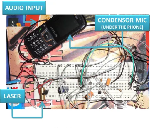
Fig. 4 Transmitter
In the fig 4, it shows the transmitter section which mainly consist of a Laser, Condenser MIC (under the phone) and here audio from the mobile phone act as input to the mic.
In the fig 5, it shows the receiver section which mainly consist of a Solar Panel, Speaker and a driver IC.
X.FUTURE ENHANCEMENT
1. Multiple voice, data, picture, video can be multiplied simultaneously to perform communication using Multiplexer. 2. Half duplex or even full duplex communication can be achieved by software implementation
3. A more power laser can be used to increase the range of communication. 4. Laser can be replaced by IR laser that can’t be visible by bare eye.
XI. CONCLUSION
The final year project “Laser based Voice and Data Communication” was completed successfully. The project completely based on wireless communication system. Although, wireless communication predominantly means the use of radio frequency for communication, we explored the use of light based carriers for transfer of information.
The emphasis of the project was to study various wireless technologies that are used for data communication between two microcontroller controlled devices. Besides this we havegained practical knowledge of microcontroller interfacing and the project software development.
Although the optical data communication technology is prevailing from last decade as optical fiber communication devices available in the market, the project was carried out to get all ideas that are behind such wireless system. And by now, we think we are successful in the respect. Also we hope our effort will be worthwhile if the project work will be hopeful for those who seek to carry out any project related to optical data communication using laser technology.
REFERENCES
[1] Mazidi Muhammad Ali, Mazzidi Janice Gillispie, “The 8051 Microntroller and Embedded Systems”, Pearson Prentice Hall. [2] Harvard B roadband Communications Laboratory.
[3] W. J. Perez H., J. Velasco Medina, D. Ravotto, E. Sanchez, M. SonzaReordaThe IEEE Workshop on Design and Diagnostics of Electronic Circuits and Systems, 2008.
[4] B-C chien, J-h Yang, W-Y. Lin, “Generating effective classifiers with Supervised Learning of Genetic Programming,” in Proc. Of the 5th international Conference on data warehousing and knowledge discovery,2003.
[5] http//www.semiconductors.philips.com
[6] A. Acampora, “Last Mile by Laser,” Scientific American, July 2002.
[7] Vikrant, Anjesh Kumar& R.S. Jha, “Comparison of Underwater Laser Communication System with