A Noval SP Kernel Finder & Kernel Composition
using Tanner Tool
Bingi Ramesh 1 & Y Praveen Kumar Reddy 2
1
M-Tech Dept of ECE, Geethanjali Engineering College NANNUR-V, KURNOOL-DIST
Mail Id:- [email protected]
2Assistant Professor Dept ECE, Geethanjali Engineering College NANNUR-V, KURNOOL
DIST Mail Id:- [email protected]
Abstract:- This paper presents an incipient methodology to engender efficient transistor
networks. Transistor-level optimization consists in an efficacious possibility to increment design
quality when engendering CMOS logic gates to be inserted in standard cell libraries. Starting
from an input ISOP, the proposed method is able to distribute series-parallel and
non-series-parallel arrangements with reduced transistor count. The experiments performed over the set of
4-input P-class Booleans functions have demonstrated the efficiency of the proposed approach.
Keywords— Logic synthesis, transistor networks, EDA, CMOS.
1. INTRODUCTION
In current VLSI design, the total number of
transistors compulsory to implement a logic
gate is vigorously cognate to the signal
delay propagation, power consumption and
area of integrated circuits (ICs). Transistor
netlists are of special interest when
designing standard cell libraries or custom
gates for ameliorating a design. To
increment design quality in full-custom
methodology, a handcraft generation of
transistor netlists for each functional block
may be performed. However, this is a
profoundly time-consuming task for more
sizably voluminous ICs, making the
adoption of such strategy prohibitive. Thus,
it becomes crucial to have available efficient
algorithms to automatically engender
optimized transistor arrangements.
In the last decades, several methods to
engender and optimize transistor networks
have been proposed. The most traditional
solutions are predicated on algebraic and
Boolean factorization. In a Boolean
expression, every instance of a variable is
called literal, and a product of literals is
formally called cube. The factorization
process manipulates a Boolean expression in
indispensable to represent a Boolean
function. Afterwards, the factored
expression is directly translated to a
transistor (switch) network. In this case,
only series and parallel (SP) arrangements
are obtained, cognate respectively to AND
and OR operations present in Boolean
expression.
Alternative methods to engender transistor
networks are predicated on graph
optimizations, where a Boolean expression
is translated to a graph. This graph can be
optimized by edges sharing or can be
gradually composed from an input
expression. In some cases, these techniques
are able to distribute better results than
factorization predicated methods if
nonseries-parallel (NSP) arrangements are
able to be found during the graph
manipulation process. Such optimization
obtained exploiting NSP topologies is due to
the immensely colossal sharing between the
paths that represent cubes of a function, so
reducing the total switch count and
surmounting SP arrangements.
This paper proposes an incipient
graph-predicated method able to engender
optimized transistor networks. Our approach
presents a structural algorithm predicated on
SP arrangements to evade dispensable
computation during the generation of
transistor networks. Different from the
approach presented in, this incipient method
distributes the networks not only applying
transistor sharing, but withal considering
topological information during the
generation process. Moreover, this paper
presents a methodology predicated on SP
kernels different from anterior method
described , in which the NSP Kernel concept
was introduced.
2. RELEATED WORK
The rudimentary element to implement a
switch network is the logic switch. This
element can be called ‘direct switch’ if it is
turned on by applying the logic value ‘1’ in
the control terminal, and ‘complementary
switch’ if it is turned on by applying the
logic value ‘0’ in the control terminal. By
composing switches, it is possible to build
arrangements, kenned as logic networks or
switch networks, in order to provide the
interconnection between two different
terminals according to a given logic function
demeanor. Depending on the technology
utilized, these switches can be implemented
as physical contrivances. In the current
the NMOS transistor (direct switch) and the
PMOS transistor (complementary switch).
When visually examining a single two
terminal network, it may present the
following properties
Planar network:- Networks corresponding
to a planar graph. This kind of graph can be
drawn in the plane without crossing lines. In
the case of networks, it is adscititiously
required that the terminals be externally
connected without crossing any lines. Planar
networks can provide a dual graph, which
has the fascinating property of being
logically and topologically complementary.
Series-parallel network:- When all
switches in the network are connected in
series or in parallel arrangements
recursively. A network is series-parallel if
and only if there is no embedded network
presenting a Wheatstone-bridge
configuration.
Bridge network:- A network with an
embedded network containing at least one
Wheatstone-bridge configuration. A bridge
network may or may not be planar, and it is
never a series-parallel network.
Bidirectional transistors – A bridge
network where transistors may conduct
current from drain to source or from source
to drain contrivance terminals according to
the input vector. That signifies the
bidirectional transistors are activated by
different logic vectors in both directions.
Supplementally, switch networks can
present two-terminals, three-terminals, or
multiple-terminals. Twoterminals networks
provide the connection between two nodes,
and are customarily applied to built
single-rail logic gates. Three-terminal networks, in
turn, are capable of annexing one node to
other two terminals, which are frequently
one for the direct polarity signal (or direct
path) and the other for the inverted polarity
signal (orcomplementary path). These ones
are exploited to design dual-rail CMOS
logic families, like DCVSL, DSL and ECDL
[9]. Multiple-terminal networks are
subsidiary to build multiple-output gates like
the Manchester chain utilized in carry
lookahead adders [10].
These characteristics are very consequential
once it is possible to build logic gates with
kindred functionality, and distinct electrical
demeanor (timing and power consumption)
to compose digital circuits by exploiting
these different switch arrangements.
3. IMPLEMENTATION
The SP Kernel Finder algorithm proposed
herein can be described as follows. For
n=|cubes(f)|, four cubes are culled by
coalescences 4 Cn . Afterwards, the
algorithm builds a graph for each
coalescence, as explicated bellow We define
an undirected graph G = (V,E) of a function
H which is given by a SOP with precisely
four cubes. The vertices in V =
{v1,v2,v3,v4} represent different cubes in
H, and |V| is the number of vertices in the
set V. An edge e = (vi ,vj) in E subsists if
and only if at least one literal appears in
both vi and vj . The operation (vi ∩ vj)
represents prevalent literals in both vi and vj
vertices. Thus, an edge e formally subsists if
and only if: (vi vj) Ø (1) We define the
label of e by utilizing label(e) = (lit(vi) ∩
lit(vj)), where lit(vi) represents the set of
literals present in vi . To ascertain that the
obtained graph is a valid SP kernel two rules
must be checked: Rule 1 – Let Evi be the set
of edges that are connected to vi . Each cube
shares all its literals if the following
equation is satiated for all v V: ⋃ (2) Rule
2 – The obtained graph must be an
isomorphic subgraph to the graph template
illustrated in Fig. 1(a). In this work this
structure is called SP kernel.
Fig 1. Vertices merging (b) and edge
reordering process (c) on a SP kernel (a).
Kernel Composition
It is consequential to descry that, depending
on the input ISOP, multiple kernels can be
found. Moreover, some cubes from the input
ISOP cannot compose any kernel. Thus, five
possible cases can occur when engendering
the transistor networks: (i) a network can be
composed by just one SP kernel; (ii) a
network can be composed by a SP kernel,
and one or more cubes that are implemented
as parallel transistor sodalities to this kernel;
(iii) a network can be composed by multiple
SP kernels in a parallel sodality; (iv) a
network can be composed by multiple SP
kernels, and one or more cubes that are
implemented as parallel transistor sodalities;
(v) there is no SP kernels and the network is
implemented through the edges sharing
algorithm. For each of these five cases, such
topological composition is done gradually
until achieving a network that is logically
During the composition process, the edges
sharing procedure is applied to the network
in order to eliminate redundant switches
[12]. Such strategy sanctions a reduction in
the total number of switches. As an example
of network generation composed by a SP
kernel and a remaining cube associated in
parallel, let us consider the following
equation: f = !a.!b.!c.!d + !a.b.!c.d +
!a.b.c.!d + a.!b.!c.d + a.!b.c.!d
For such ISOP, the SP Kernel Finder routine
founds the SP kernel illustrated in. This
kernel may be mapped to the transistor
network illustrated in Fig. 3(b). Besides that,
the cube !a.!b.!c.!d was not implemented
through the found kernel. Hence, this cube
must be associated in parallel with such
kernel as. In the next, the SP kernel and the
remaining cube are gradually merged, by
applying the edges sharing procedure,
resulting in the sharing of the switch !a
depicted by the Fig. e1 e3 e2 e4 e2 e1 e4 e3
e2 e1 e4 e3 c a b d a c d b a.c b.c d.b a.d .
Afterwards, the redundant switch !c is
shared, resulting in the optimized switch
network presented in.
Figure 2. SP kernel (a) obtained from the
Equation (4) and resultant network (b).
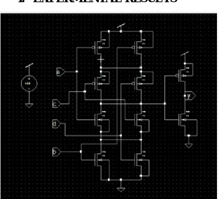
4. EXPERMENTAL RESULTS
Fig:-4 Simulation Resluts
Fig:-5 Statical Results
5. CONCLUSION
This paper proposed an incipient
graph-predicated method to engender optimized
transistor (switch) networks. The proposed
method results in a reduction of transistor
count when compared to antecedent
approaches. It is kenned that reducing
transistor count in a logic gate it is possible
to achieve better results in terms of signal
delay propagation and power consumption.
These associated gains were not explicitly
investigated in this work, and they are being
left as future work at gate, library and circuit
design level.
6. REFERENCES
[1] B. H. Calhoun, Yu Cao, Xin Li, Ken
Mai, L. T. Pileggi, R. A. Rutenbar, and K. L.
Shepard, “Digital circuit design challenges
and opportunities in the era of nanoscale
CMOS”, IEE Proccedings, vol. 96, no. 2, pp.
343-365, Feb. 2008.
[2] M. G. A. Martins, L. S. Rosa Jr., A. B.
R. Rasmussen, R. P. Ribas, and A. I. Reis,
“Boolean factoring with multiple objective
goals”. ICCD 2010, pp. 229-234.
[3] V. Callegaro, L. S. Da Rosa Jr., A. I.
Reis, and R. P. Ribas, “A Kernel-based
approach for factoring logic functions,”
Microelectronics Students Forum, 2009.
[4] J. Zhu and M. Abd-El-Barr, “On the
optimization of MOS circuits,” IEEE Trans.
on Circuits and Systems, vol. 40, no. 6, pp.
412-422, June 1993.
[5] D. Kagaris and T. Haniotakis, “A
methodology for transistor-efficient
Systems, vol. 15, no. 4, pp. 488-492. Apr.
2007.
[6] R. Roy, D. Bhattacharya, V. Boppana,
"Transistor-level optimization of digital
designs with flex cells," IEEE Trans. on
Computers , vol.38, no.2, pp. 53- 61, Feb.
2005.
[7] M. C. Golumbic, A. Mintz, U. Rotics,
“An improvement on the complexity of
factoring read-once Boolean functions”,
Discrete Appl. Math, 2008, Vol. 156, n. 10,
p. 1633-1636.
[8] E. Sentovich et al, “SIS: A system for
sequential circuit synthesis”, Technical
Report No. UCB/ERL M92/41, EECS
Department, University of California,
Berkeley, 1992.
[9] M. G. A. Martins, L. S. Da Rosa Junior,
A. Rasmussen, R. P. Ribas, A. I. Reis,
“Boolean Factoring with Multi-Objective
Goals”. In: IEEE Int. Conf. on Computer
Design (ICCD 2010), p. 229-234.
[10] J. Zhu, M. Abd-El-Barr, “On the
optimization of MOS circuits”. IEEE Trans.
on Circuits and Systems: Fundamental
Theory and Applications, Theory Appl., vol.