Impact of Fin Dimensions on Performance of
Adder and Subtractor
Rahil Kumar1, Kanika Sharma2, Ravi Goel3
PG Student [VLSI], Dept. of ECE, Faculty of Engineering and Technology, MRIU, Faridabad, India1 PG Student [VLSI], Dept. of ECE, Faculty of Engineering and Technology, MRIU, Faridabad, India2 Assistant Professor, Dept. of ECE, Faculty of Engineering and Technology, MRIU, Faridabad, India3
ABSTRACT: The FinFET architecture has emerged a viable contender for the ultimate scalability of CMOS devices. FinFET structure offers better control over device leakage currents than the conventional bulk MOSFET structure. In this work the adder and subtractor implementation using 30 nm technology. The figure of merit measure for adder and subtractor are power and delay. Based on the simulation results, it is found that the fin thickness (Tfin), fin height (Hfin) are very important deciding factor for power and delay. There is a phenomenal increase in short channel effects when the fin dimensions are increased. From the simulation average power is calculated for the variation in Hfin for full adder and full subtractor to 34% and 24 % when the height of fin is minimum while in case when height is maximum the average power of full adder and full subtractor is increased to 51% and 26% respectively. On the other hand power increases 14% and 16% when Tfin is maximum for full adder and subtractor respectively. And when Tfin is minimum power reduces to 21% and 24% respectively. Delay calculation for different values of Hfin for full adder and full subtractor is 17 % and 16% increase in delay when Hfin is minimum.while for maximum value of Hfin delay isreduced to 58% and 27% respectively. Similarly delay for full adder and full subtractor is 13% and10% increase when Tfin is minimum and for maximum values of Tfin delay reduces to 10% and 15% respectively.
KEYWORDS: FinFET, Adder, Subtractor, circuit design, device simulation, Hspice, Parameter variation.
I. INTRODUCTION
Figure 1: Basic structure of finFET
The wrap around structure provide a better electrical control over the channel and thus help to reducing the leakage current and overcoming short channel effect. In the finFET the silicon body has been rotated on its edge into a vertical orientation so only source and drain regions are placed horizontally about the body as in a conventional planner FET. The saperate biasing in dual gate device easily provide multiple threshold voltages. A gate can also be fabricated at the top of the fin, in which case it is triple gate FET, The width of the finFET is quantised due to a vertical gate structure. The fin height determine the minimum transistor width(Wmin) with the two gate of the single FET tied together, Wmin is
Wmin = 2*Hfin+ Tfin
Where Hfin- height of the fin, Tfin- thickness of the si body. FinFET are designed to use multiple fin to achieve larger channel width[4]. Source/drain pads connect the fin in parallel as the no. of fins is increased, the current through the device increases For high layout density, the ratio between fin height and the achievable pitch between to successive fins has to be maximized[5]. In particular the fin height has to be higher than the pitch between the fingers in order to obtained the same drive current per silicon area as per planar double gate transistors to improve the ratio with respect to the pitch achievable by lithography, the use of spacer or hard mask for the fin patterning can be use that way the fin density can be doubled[13]. FinFET offers distinct advantages for scaling to very short gate lengths[7]-[8]. Fabrication of the FinFET is similar to conventional CMOS process, with only minor disruptions, offering the potential for a rapid deployment to manufacturing. The channel of the FinFET is a tiny chunk of undoped silicon perpendicular to the substrate[9]. The control of short channel effects for FinFETs is provided by the two gates without aggressively scaling down the gate-oxide thickness and increasing the channel doping density. Also the finFET come in many varients like shorted gate(SG) mode, Independent gate(IG) mode, low power (LP) mode and hybrid mode (IG/LP). In shorted gate(SG) mode of operation, the two gates are biased together to turn on the device, providing maximum gate drive. In the Independent gate(IG) mode of operation, the two gates are electrically independent[9]. In Low power(LP) mode of operation the back gate is tied to a reverse-bias voltage to reduce leakage power. In hybrid mode of operation IG and LP modes are combined[11].
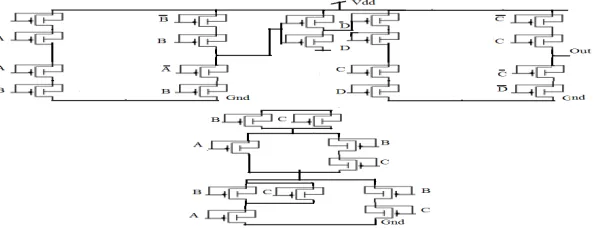
II. DESIGN OF FULL ADDER AND SUBTRACTOR
Full Adder
A full adder is a combinational circuit that forms the arithmetic sum of three input bits. It consists of three inputs and two outputs. In this design, the designated three inputs are A, B and Cin. The third input Cin represents carry input to the first stage. The output are SUM and CARRY. The Boolean expression for SUM and CARRY bits are given below.
SUM = A xor B xor C CARRY = AB+ BCin + CinA
Figure 2. Transistor level diagram of full adder
Full Subtractor
A full subtractor is a combinational circuit that performs a subtraction between two binary bits and ‘1’ may have been borrowed by a lower significant stage. This circuit has three inputs and two outputs. In this design the designated three inputs are A,B and Bin. The third input Bin represent the borrow input to the first stage. The outputs are DIFF and Bout. The Boolean expression for DIFF and Bout bits are given below.
DIFF = A B Bin Bout = AB + ABin + BBin
The transistor level diagram of full subtractor is shown below in Figure 3.
Figure 3. Transistor level diagram of full subtractor
Variation in Dimensions of FinFET
The parameters considered here are height of fins (Hfin), thickness of fins (Tfin). These parameters are varied over a range of values to capture their effect on average power and delay. Here in Table 1 show the values of the parameters for 30nm are.
Table 1. FinFET device perameters and their variations
Parameter Value Variation
Thickness of fin (Tfin) (nm) 15 5 – 20
Height of fin (Hfin) (nm) 30 20 – 40
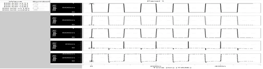
The Input and output waveform of 1-bit adder are shown below in Figure 4 .According to the input signal provided as A B and Cin the outputs sum and CARRY were properly generated verified with truth-table of full adder..
Figure 4. Transient analysis of full adder
Transient response of input and output oo 1-bit subtractor is shown below in Figure 5 where A.B and C are the inputs and diff., bout are outputs.
Figure 5. Transient analysis of full subtractor.
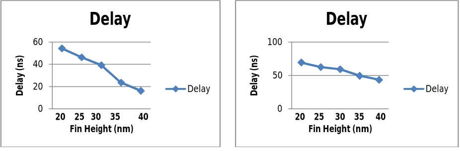
Effect of Fin Height on Delay and power
Here the fin height (Hfin) is varied as 20nm, 25nm, 30nm, 35nm, 40nm. As fin height decrease, leakage current decreases because of increase in its parasitic resistance (Rp). So that the reduction in power leakage and delay should be increased as the height of the fin decreases, while on the other hand when Hfin increased the current drive also increase due to increase in the gate area so the delay reduced but it also increase the gate leakage resulting the increase in power dissipation. Table 2 below shows the variation in average power at different value of Hfin.
Table 2. Variation in average power for full adder and full subtractor
Fin Height 20nm 25nm 30nm 35nm 40nm
Full subtractor 0.85pw 1,07pw 0.097nw 0.149nw 1.719nw
Full adder 0.55pw 2.18pw 0.041nw 0.519nw 1.62nw
Figure 6. The effect of Fin Height on a) Average power of full adder b) Average power of full subtracton
As the height of the fin increases it will impact on delay started to reduce because of the increase in drive current throught the gate. Table 3 show the variation in delay at different values for Hfin.
Table 3 Variation in Delay for different values of Hfin
Fin Height 20nm 25nm 30nm 35nm 40nm
Full adder 54.2ns 46.2ns 39.1ns 23.6ns 16.2ns
Full subtractor 69.23ns 62.4ns 59.1ns 49.4ns 43.4ns
The effect of Fin height on delay is shown in Figure 7 below a) for full adder and b) for full subtractor. It show that as the value of Hfin is increases the delay started to reduce while is the Hfin is reduces it also increase the delay.
Figure 7. Effect of Fin Height on a) Delay of full adder b) Delay of full subtractor.
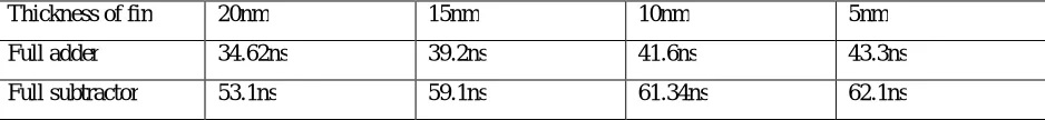
Effect of Thickness of Fin on Delay and Power
The thickness of Fin is varied as 5nm, 10nm, 15nm, 20nm. Leakage current increases with increase in fin width due to reduced control of the gate over the channel because the leakage current occurs at the middle of the fin, which is the more remote area from the gate. But as fin width decreases, the middle part of the fin has more control from the gate, so the leakage current decreases. Table 4 below show the variation in average power for different values of Tfin.
1.00E-13 1.00E-10 1.00E-07 1.00E-04 1.00E-01 A ve ra ge P o w e r (n w )
20 25 30 35 40 Fin Height (nm)
Average power
Average power 1.00E-13 1.00E-10 1.00E-07 1.00E-04 1.00E-01 A ve ra ge P o w e r (n w )20 25 30 35 40 Fin Height (nm)
Average power
Average power 0 20 40 60 D e la y (n s)20 25 30 35 40 Fin Height (nm)
Delay
Delay 0 50 100 D e la y (n s)20 25 30 35 40 Fin Height (nm)
Delay
Thickness of fin 20nm 15nm 10nm 5nm
Full subtractor 0.144nw 0.0337nw 0.0127nw 2.64pw
Full adder 0.115nw 0.0419nw 5.12pw 1.43pw
The graph in Figure 8 shows that as Tfin is increased the due to increase in leakage power also increases while as the reduces the Tfin the power stated to decrease .
Figure 8. Effect of Thickness of Fin on a) average power of full adder b) average power of full subtractor.
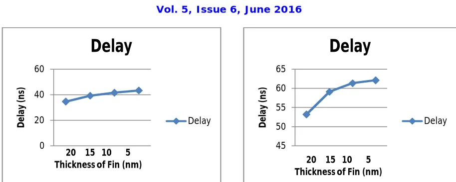
The effect of thickness of fin on the delay of full adder is shown below in Table 5 which shows that as the thickness of the fin is increases delay started to decrease while decreasing the value of Tfin delay is increasing due to more current drive through the channel delay is decreased while as the Tfin decreases it reduces the current drive resulting increase in delay. Similarly for full subtractor.
Table 5. Variation in average power for different values of Tfin
Thickness of fin 20nm 15nm 10nm 5nm
Full adder 34.62ns 39.2ns 41.6ns 43.3ns
Full subtractor 53.1ns 59.1ns 61.34ns 62.1ns
The graphical representation for the different values of Tfin for delay when Tfin is at maximum value the delayis at minimum value but as the value of Tfin is reduces it changes the value of delay and it stated to increases as the Tfin reduces.Figure 9 below shows variations for full adder and subtractor respectively.
0.00E+00 5.00E-11 1.00E-10 1.50E-10
A
ve
ra
ge
p
o
w
e
r
(n
w
)
20 15 10 5 Thickness of Fin (nm)
Average power
Average power
0.00E+00 5.00E-11 1.00E-10 1.50E-10
A
ve
ra
ge
p
o
w
e
r
(n
w
)
20 15 10 5 Thickness of Fin (nm)
Average power
Figure 9. a) Effect of Thickness of Fin on a) Delay of full adder b) Delay of full subtractor.
IV. CONCLUSION
The design of the Full adder and full subtractor has been designed by using finFET. The design is perform in 30nm technology. The effect of the dimensions of the FinFET on 1-bit full adder and 1-bit full subtractor is shown. The delay and power is calculated for different values of Hfin and Tfin. Which shows that change in the dimensions of the device can also effect the performance of the device the power is calculated for the variation in Hfin for full adder and full subtractor when fin height is minimum the power is reduced to 34% and 24 % while in case when height is maximum the average power of full adder and full subtractor isincreased to 51% and 26% respectively. On the other hand when Tfin is varied the change in average power for full adder and full subtractor when Tfin is maximum power increased 14% and 16% and when Tfin is minimum power reduces to 21% and 24% respectively. Delay calculation for different values of Hfin for full adder and full subtractor when hfin is minimum is 17 % and 16% increase in delay.while for maximum value of Hfin delay is 58% and 27% respectively. And change in delay for full adder and full subtractor when Tfin is minimum is 13% and10% and for maximum values of Tfin is 10% and 15% respectively.
REFERENCES
1. Farhana Sheikh Vidya Varadarajan, “ The impact odf device-width quantization on digital circuit design using finFET structure” , International conference on Computer aided design, EE 241 spring 2004.
2. Seung-Hwan Kim and Jerry G. Fossum, fellow, IEEE, “Design Optimization and performance projection of double gate FinFETs with gate-Source/Drain underlap for sram Application” , IEEE transction on electron devices, vol.54, No.8, August 2007.
3. Ajay N Bhoj, student member, IEEE, and Niraj K Jha, Fellow,IEEE ,” Design of logic gates and flip flops in high performance finFET Technology”, IEEE Transaction on very large scale integration system,vol. 21, no. 11, November 2013.
4. Masoud Rostami, Student member, IEEE, and Kartik Mohanram, Member, IEEE, “Dual -Vth Independent gate FinFET for low power logic circuits”, IEEE Transaction on computer aided design of integrated circuits and systems, vol. 30. No. 3 March 2011.
5. Michael C Wang, Princiton university, “ Low power, Area Efficient FinFET Circuit Design”, proceedings of the world congress on engineering and computer science 2009 vol. 1WcECS October 20-22 2009, San Francisco, USA.
6. Prateek Mishra, Anish Muttreja, and Niraj K. Jha, “ FinFET Circuit Design”, Nanoelectronics circuit Design, Springer science business medi, LLC 2011.
7. Jean-Pierre Colinge , “FinFET and Other Multi-Gate Transistors”, Integrated circuits and systems, Springer.
8. A.Amara, O.Rozeau, “Planar Double-Gtae Transistor”, springer science + Business Media B.V., ISBN 978-1-4020-9327-2, pp.17-18, 2009. 9. Jency Rubia J., Gopal B.G., Prabhu V. ” Analysis, Design and implementation of 4-bit Full adder using FinFET”, Journal of convergence
Information Technology (IJCT), vol. 10, no. 2, March 2015.
10. M.Onabjo and J. Silva-Martinez, “ Process variation Challenges and solutions Approaches”, springer science + Business Media New York, ISBN 978-1-4614-2296-9_2, 2012.
11. Likhitha Dhulipalla, Lourts Deepak.A, “Design And Implementation Of 4-Bit ALU Using FinFETs For Nano Scale Technology,” Nanoscience Engineering and Technology (ICON SET), 2011 International Confrence, pp. 190-195, 2011.
12. Jakub Kedziersk, Meikei Ieong, Edward Nowak, Thomas S.Kanarsky, Ying Zhang, Ronnen Roy, Diane Boyd, David Fried, and H.-S. Philip Wong, “Extension And Source/Drain Design For High-Performance FinFET Devices,” IEEE Transactions on Electron Devices, Vol. 50, No.4, pp. 952-958, April 2003.
13. Prateek Mishra and Niraj K. Jha, “Low-Power FinFET Circuit Synthesis using Surface Orientation Optimization”, Princeton University, Princeton, NJ 08544.
0 20 40 60 D el a y (n s)
20 15 10 5 Thickness of Fin (nm)
Delay
Delay 45 50 55 60 65 D el a y (n s)20 15 10 5 Thickness of Fin (nm)
Delay
Rahil kumar received his bachelor degree in electronics and communication engineering from uttarakhand technical university in 2013. M.Tech, VLSI& Embedded system, Manav Rachna International University, Faridabad, Haryana. His area of interest include VLSI technology, nanoscale cmos devices.
Kanika Sharma received her Bachelor degree in Electronics and Communication engineering from Echelon Institute of Technology, Faridabad, Haryana in 2014. M.Tech , VLSI& Embedded system, Manav Rachna International University, Faridabad, Haryana. Her areas of interest include VLSI technology and CMOS devices designing.
Mr. Ravi Goel did his M.tech in VLSI from NIT Hamirpur Himanchal pradesh. His area of interest is low power VLSI. Presently he is working as assistant professor at Faculty of Engineering and Technology, MRIU Faridabad.