Design and FPGA Implementation of
Modified DA Based Processor for Image
Compression
M.Arun, R.Krishnaveni, K. Banumathi , A.Selva Agnes
Assistant Professor, Dept of ECE, Panimalar Institute of Technology, Chennai, India1,2,3,4
ABSTRACT: Image compression is one of the method which are widely used in areas such as medical, automotive, consumer and military. Discrete wavelet transforms is the most widely used transformation technique that is adopted for image compression. DWT is always high due to large number of arithmetic operations it is highly complex. In this work a modified Distributive Arithmetic based DWT architecture is proposed and is implemented on FPGA. This design is two times faster than the reference design and is thus suitable for applications that require high speed image processing algorithms.The proposed method is implemented in FPGA.
KEYWORDS: DWT,FPGA,Image Compression.
I.INTRODUCTION
Technological growth of semiconductor industry has led to unprecedented demand for low power, high speed complex and reliable integrated circuits for medical, defense and consumer applications. Today's electronic equipment comes with user friendly interfaces such as keypads and graphical displays. As images convey more information to a user, it is many of the equipment today have image displays and interfaces. Image storage on these smaller, handled devices is a challenge as they occupy huge storage space; also image transmission requires higher bandwidth. Hence most of the signal processing technologies today has dedicated hardware’s that act as co-processors to compress and decompress images. In this work, a reliable, high speed, low power DWT-IDWT.
Processor is designed and implemented on FPGA which can be used as a co-processor for image compression and decompression.
The Discrete Wavelet Transform (DWT) is being increasingly used for image coding. This is because the DWT can decompose the signals into different sub-bands with both time and frequency information. It also supports features like Progressive image transmission, compressed image manipulation, and region of interest coding. Recently several VLSI architectures have been proposed to realize single chip designs for DWT. Traditionally, such algorithms are implemented using programmable DSP chips for low-rate applications, or VLSI application specific integrated circuits (ASICs) for higher rates. In wavelet Transforms, the original signal is divided into frequency resolution and time resolution contents.
In this brief, we propose a novel methodology for memory reduction in the DA-based design of the DWT/IDWT architecture by exploiting its inherent algorithmic symmetry resulting in data repeatability. Subsequently, a 16-b fixed-point DWT/IDWT architecture is developed for a frame length of 16, which requires significantly less silicon area and power consumption compared to some of the published DWT/IDWT architectures. The rest of this brief is organized as follows.
II. LITERATURE REVIEW
David S. Taubman, Michael W. Marcellin – “JPEG 2000 – Image compression, fundamentals, standards and practice", Kluwer academic publishers, second printing – 2002.
JPEG2000: Image Compression Fundamentals, Standards and Practice is written in four parts. Representing about half the total text, Part I of the book provides a thorough and up-to-date background in the fundamentals of image compression, including topics not previously brought together in a single volume. Part 2 contains a complete description of the JPEG2000 standard. This description is written in such a way as to be completely self-contained from an implementation perspective, while it contains numerous references to the fundamental developments in Part 1. Together, Parts 1 and 2 serve the complementary roles of explanation and exposition in relation to both the JPEG2000 standard and modern image compression techniques. Part 3 of the book is devoted to the implementation and exploitation of the JPEG2000 standard, containing guidelines, suggestions, and analyses for both software and hardware oriented applications. Part 4 describes other key image compression standards, namely JPEG and JPEG-LS. The purpose of this material is to allow the reader to compare the capabilities and complexity associated with these standards with those of JPEG2000. This final part of the book also serves to provide a practical demonstration of some of the fundamental techniques introduced in Part 1 which are not demonstrated by the JPEG2000 standard.
G. Knowles, "VLSI Architecture for the Discrete Wavelet Transform," Electronics Letters, vol.26, pp. 1184-1185, 1990.
The wavelet transform is a very effective signal analysis tool for many problems for which Fourier based methods have been inapplicable, expensive for real-time applications, or can only be applied with difficulty. The discrete wavelet transform can be implemented in VLSI more efficiently than the FFT. A single chip implementation is described.
M, Vishwanath, R. M. Owens, and M. J. Irwin, "VLSI Architectures for the Discrete Wavelet Transform," IEEE Trans. Circuits And Systems II, vol. 42, no. 5, pp. 305-316, May. 1995
This paper present an area-efficient storage and routing structure to be used as part of either a DWT or an IDWT filter. Such efficient structures are necessary for the single chip implementation of multidimensional DWT and IDWT filters for processing images and video. While the storage structures described in previously published architectures were adequate for the 1D DWT/IDWT filter, they do not scale well to a multidimensional implementation. The storage structure design and implementation described in this paper utilizes a combination of well-known efficient RAM cells with simple control to achieve compact size and scalability. When compared to other alternatives, the structure uses less power.
This paper also examines the problem of constructing, on a single chip, filters for both the multidimensional Discrete Wavelet Transform (DWT) and the multidimensional Inverse Discrete Wavelet Transform (IDWT).
It considers a network with N mobile unlicensed nodes that move in an environment according to some stochastic mobility models. It also assumes that entire spectrum is divided into number of M non-overlapping orthogonal channels having different bandwidth.
The access to each licensed channel is regulated by fixed duration time slots. Slot timing is assumed to be broadcast by the primary system. Before transmitting its message, each transmitter node, which is a node with the message, first selects a path node and a frequency channel to copy the message.
coordination packet that is generated by a node with message is to inform its path about the frequency channel decided for the message copying.
III. METHODOLOGY
3.1 Motivational Example
The basic DA equation can be given
1 0 , , .,
2
.
2
i b b b n l l n
n
x
x
x
where l = (total number of bits per sample). In dyadic space, a convolution-based wavelet filter can be represented as
n n a n ax
h
w
2where xn and hn are input samples and filter coefficients, respectively. Considering frame-length = 4 and wordlength = 4 (as an example) and using (1) in (2) with a = 1, we get
3 2 0 , 0 1 0 , 1 0 0 , 2 3 2 3 , 0 1 3 , 1 0 3 ,
2
]
2
...
[
]
2
[
x
h
x
h
x
h
x
h
x
h
x
h
w
a
where xij is the ith sample’s jth bit of the input data. The possible combinations of filter coefficients obtained from are shown in the first six rows of Table I, which occupies 16 memory locations. However, it can be observed in Table I that there exists redundant (such as “0”) and repetitive filter coefficients (such as “h0,” “h1,” “h2,” “h1 + h2,”
“h0 + h1,” “h0 + h2,” and “h0 + h1 + h2”) occupying more than a single memory location. Thus, if only the unique
combinations of the filter coefficients are stored in the memory, the other filter coefficients can be obtained on the fly using simple addition operations. In this particular example, the proposed methodology leads to only four memory locations, as shown in the last two rows of Table I, rather than 16 locations in the conventional approach.
However, reducing memory at the expense of adders raises two particular issues. First, a new addressing scheme needs to be formulated to address the reduced memory system. Second, the hardware savings obtained due to the reduction in memory size can be negated if the total number of adders used in the design is more than a certain limit.
IV. ARCHITECTURAL OVERVIEW
The block diagram of the DWT/IDWT architecture is shown in Fig. At the block level, the architecture is similar to a standard DA-based architecture. However, the main novelty of the architecture lies in the formulation of a new addressing scheme and the corresponding address generation unit design for the reduced memory unit.
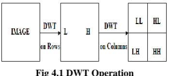
Fig 4.1 DWT Operation
4.1 Memory Unit
frame length 16 for the first resolution level of the analysis bank. Fig. shows the incoming data samples and the associated filter coefficients required for computing each wavelet coefficient in this case. It can be noted from Fig. 2 that the filter coefficients are the same for the different samples present in the same inclined slices. For example, as shown in the encircled regions in Fig. , the filter coefficients associated with the samples for computing the third wavelet coefficient are the same for the last five samples of the fourth wavelet coefficient computation. Mathematically, the filter coefficients associated with the qth data sample of the rth and (q + 2)th data samples of the (r
+ 1)th wavelet coefficients are the same (symmetry property). This symmetry can be represented in generalized form for the ith level of resolution.
There are several architectures for realizing the DWT shown in Fig, paper summarizes various schemes. Most popular one is the DA-DWT scheme that is suitable on FPGA, as it consumes fewer resources and has high through put. DA-DWT architecture based on pipelining and parallel processing logic is realized and implemented on FPGA. In this work, a modified DA-DWT architecture is designed based on the work reported in.
The number of LUTs and number of shift registers are reduced by exploiting the symmetric property of the 917 wavelet filters. Efficient fixed point number representation scheme is identified to accurately represent the 917 filter values and are stored in the LUT
memory space on FPGA. A control logic designed loads the input data into the FPGA from the external memory, LUT contents are read out based on the input samples as address to LUT. After 8 clock cycles of initial latency, DWT outputs are computed every clock cycle. Software reference model for DWT-IDWT processor is built using Matlab. Multiple image test vectors are used in analysing the performances of the software reference model.
V. DISTRIBUTIVE ARITHMETIC BASED 2D DWT/IDWT ARCHITECTURE
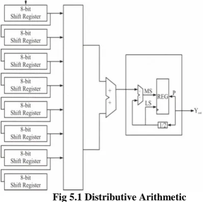
In this section, we first outline how to perform multiplication by using memory based architecture. Following this, we briefly explain architecture for DWT filter bank. Using this we show complete design for block based DWT. The memory based approach provides an efficient way to replace multipliers by small ROM tables such that the DWT filter can attain high computing speeds with a small silicon area as shown in Fig. Traditionally, multiplication is performed using logic elements such as adders, registers etc.
However, multiplication of two n-bit input variables can be performed by a ROM table of size of 22n entries. Each entry stores the pre-computed result of a multiplication. The speed of the ROM lookup table is faster than that of hardware multiplication if the look-up table is stored in the on-chip memory. In DWT, one of the input variables in the multiplier can be fixed. Therefore, a multiplier can be realized by 2n entries of ROM.
Fig 5.1 Distributive Arithmetic
position. This scheme reduces the memory size to half due to the symmetric property of the filter coefficients. This increases the through put as the input samples are simultaneously used to read the data from two LUTs and hence speed is increased.
Fig 5.2 Parallel implementation of DA technique
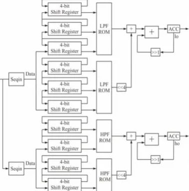
VI MODIFIED DA-DWT ARCHITECTURE:
The modified DA-DWT architecture shown in Fig consists of four LUTs, each of the LUTs are accessed by the even and odd samples of input matrix simultaneously. Odd and even input samples are divided into 4 bits of LSB and 4
Bits of MSB, each 4-bit data read the content of four different LUTs that consist of partial products of filter values computed and stored as per the DA logic. Input samples are split into even and odd in the first stage, the data is further loaded
Sequentially into the serial in serial out shift registers, top four shift register store MSB bits and bottom four shifts register stores the LSB bits. It requires 40 clocks cycles to load the shift register contents. At the end of 40th clock cycle, the control logic configures the shift register as serial in parallel out, thus forming the address for the LUT. The partial products stored in the LUT are read simultaneously front all the four LUTS and are accumulated with previous values
Available across the shift register in the output stage. The output stage consisting of adders, accumulators and right shift registers are used to accumulate the LUT contents and thus compute the DWT output. This architecture has a latency of 44 clock cycles in computing the first high pass and low pass filter coefficients, and has a through put of 4 clock cycles. This architecture is faster by the previous architectures as the latency is reduced by half clock cycles and through put is increased by a factor of 2.
VII. RESULT AND DISCUSSION
7.1 Practical Parallel implementation of DA technique
Spartan-3E FPGA
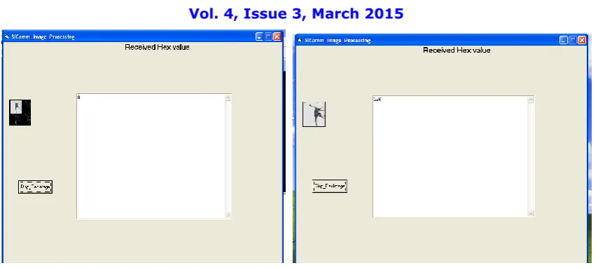
The fig 7.1 shows the implementation of Image compression using a FPGA KIT.
Fig 7.1 Spartan-3E FPGA
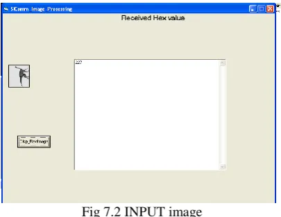
Input Image Received
The fig 7.2 shows the input dino image that is taken for compression using DWT.
Fig 7.2 INPUT image DWT Performed Output
The fig 7.3 shows the DWT Performed Output for input dino image that is taken for compression using DWT.
Reconstructed Output
Fig7.3 DWT of input image Fig 7.4 Reconstructed output
VI.CONCLUSION
The Discrete Wavelet Transform provides a multi resolution representation of images. The transform has been implemented using filter banks. For the design, based on the constraints the area, power and timing performance were obtained. Based on the application and the constraints imposed, the appropriate architecture can be chosen. The proposed architecture is twice faster than the reference design. It is seen that, in applications, which require low area, power consumption, and high throughput, e.g., real-time applications. The biorthogonal wavelets, with different number of coefficients in the low pass and high pass filters, increase the number of operations and the complexity of the design, but they have better SNR than the orthogonal filters. First, the code was written in VHDL and implemented on the FPGA using a 64 x 64 random image. Then, the code was taken through the ASIC design flow. For the ASIC design flow, 8x8 memory considered to store the image. This architecture enables fast computation of DWT with parallel processing. It has low memory requirements and consumes low power. By using the same concepts which are mentioned above are useful in designing the Inverse Discrete Wavelet Transform (IDWT).
REFERENCES
[1] David S. Taubman, Michael W. Marcellin - JPEG 2000 – Image compression, fundamentals, standards and practice", Kluwer academic publishers, Second printing - 2002.
[2] G. Knowles, "VLSI Architecture for the Discrete Wavelet Transform," Electronics Letters, vo1.26, pp. 1184-1185,1990.
[3] M, Vishwanath, R. M. Owens, and M. 1. Irwin, "VLSI Architectures for the Discrete Wavelet Transform," IEEE Trans. Circuits And Systems II, vol. 42, no. 5, pp. 305-316, May. 1995.
[4] AS. Lewis and G. Knowles, "VLSI Architectures for 2-D Daubechies Wavelet Transform without MUltipliers". Electron Letter, vo1.27, pp. 171-173, Jan 1991.
[5] K.K. Parhi and T. Nishitani "VLSI Architecture for Discrete Wavelet Transform", IEEE Trans. VLSI Systems, vol. 1, pp. 191-202, June 1993. [6] M. Vishwanath, R.M. Owens and MJ. Irwin, "VLSI Architecture for the Discrete Wavelet Transform", IEEE Trans. Circuits and Systems, vol. 42, pp. 305-316, May 1996.
[7] C. Chakrabarti and M. Vishwanath, "Architectures for Wavelet Transforms: A Syrvey", Journal of VLSI Signal Processing, Kulwer, vol.lO, pp. 225-236,1995.
[8] David S. Taman and Michael W. Marcelliun, "JPEG 2000 – Image Compression, Fundamentals, Standards and Practice", Kulwer Academic Publishers, Second printing 2002.
[9] Charilaos Christopoulos, Athanassios Skodras, and Touradj Ebrahimi - "THE JPEG2000 STILL IMAGE CODING SYSTEM – AN OVERVIEW", Published in IEEE Transactions on Consumer Electronics, Vol. 46, No. 4, pp. 1103-1127, November 2000.
[10] Majid Rannani and Rajan Joshi, "An Overview of the JPEG2000 Still Image Compression Standard", Signal Processing, Image Communication, vol. 17, pp. 3-48, 2002.