Thesis for the degree
Master of Science
By
Yossef Oren
Advisor
Professor Adi Shamir
August 2006
Submitted to the Scientific Council of the
Weizmann Institute of Science
Rehovot, Israel
קוחרמ קפסה תפיקת
יגת לש
RFID
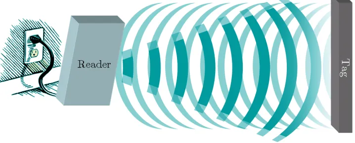
Remote Power Analysis of RFID Tags
ראותה תלבק של רובח
יעדמל מסומ
תאמ
ןרוא ףסוי
החנמ
רוספורפ
רימש ידע
סשת לולא
"
ו
לש תיעדמה הצעומל שגומ
עדמל ןמציו ןוכמ
תובוחר
,
Remote Power Analysis of RFID Tags
Abstract
We describe the rst power analysis attack on passive RFID tags. Compared to standard power analysis attacks, this attack is unique in that it requires no physical contact with the device under attack. The power analysis can be carried out even if both the tag and the attacker are passive and transmit no data, making the attack very hard to detect.
As a proof of concept, we use power analysis to extract the kill passwords from Class 1 EPC tags operating in the UHF frequency range. Tags from several major vendors were successfully attacked. Our attack can be extended to HF tags and to remote fault analysis.
The main signicance of our attack is not in the discovery of kill passwords but in its implications on future tag design any cryptographic functionality built into tags needs to be designed to be resistant to power analysis, and achieving this resistance is an undertaking which has an eect both on the price and on the performance of tags.
Acknowledgements
I am truly thankful for having the opportunity to work on such an exciting topic of research. The results presented here are the result of collaboration with many people, and would not have been possible if not for the generosity and guidance of those who helped me along the way.
First of all, I am indebted to my dear wife Michal for encouraging me to take on M.Sc studies and for enduring two years of living on scholarship. I thank her and both sets of grandparents for the countless hours they invested.
Simon Krausz found enough time in his impossible schedule to pass my idea through its rst trial by re. Oren Zarchin and his colleagues at Prof. Moti Heiblum's lab taught me how to use a spectrum analyser. Oded Smikt, the de-partment's engineer and tinker (and master of the dede-partment's apparently endless stockrooms) eliminated the MacGuyver element from my lab setup and helped me get some results instead of a nasty electric shock. Daniel Dobkin provided me with many crucial hints regarding my research, both through personal communications and through the WJ Communications online forum. Mickey Cohen reviewed the initial version of this work and helped make it more palatable to people outside the cryptographic community. Ari Juels provided me with the idea for the attack on Generation 2 devices and helped me understand its consequences. Eran Tromer jump-started my project more than once with his many helpful suggestions and constant encouragement (I'm just glad his optimism was justied). I would also like to thank Eli Okon for helping me set up the lab, Gideon Yuval for pointing out the password guessing attack on TENEX and Prof. Oded Goldreich for the shidduch. I thank the Feinberg Graduate School and the Department of Com-puter Science of the Weizmann Institute for funding my studies through the past two years. I would also like to thank my roommates for coping with the noise, wierd gear, wandering screws and perfectly safe radiation. There are many others I thank them all for kindly sharing their knowledge, time and equipment.
I would especially like to thank Prof. Adi Shamir for constantly challenging me with impossible goals and helping me meet them, for providing his ideas and his experience and most of all for his enthusiasm. It was truly an honour and a pleasure to work with Prof. Shamir.
4 ACKNOWLEDGEMENTS
Finally, I would like to dedicate this work to the people of Gush Katif. I hope that we will all be oered consolation through the building of Jerusalem.
Contents
Abstract 1
Acknowledgements 3
List of Figures 9
Chapter 1. Introduction 11
1.1. The RFID Tag the World's Simplest Computer 11
1.1.1. General Structure of an RFID System 11
1.1.2. A Taxonomy of RFID Systems 12
1.1.3. The Case for Security in RFID Present and Future 14
1.2. Side-Channel Cryptanalysis 14
1.2.1. Power Analysis 15
1.2.2. Protection from Side-Channel Attacks 16
1.3. Our Contribution 16
1.4. Structure of this Document 17
Chapter 2. Previous Work 19
2.1. Password Guessing Attacks 19
2.2. Power Analysis of Smart Cards and Other Cryptosystems 19
2.3. Remote EM-based Attacks 19
2.3.1. Screen Sning 20
2.3.2. Smart card Emanations 20
2.4. Attacks on RFID Tags 21
2.4.1. The RFID Threat Model 21
2.4.2. Current Attacks on RFID Tags 21
Chapter 3. Theoretical Background 23
3.1. The EPC Standard Family 23
3.1.1. The Physical Layer 24
3.1.1.1. The General Structure of a Tag 24
3.1.1.2. Frequencies and Power Levels 25
3.1.1.3. Power Supply to Passive Tags 26
3.1.1.4. Data Transfer from Reader to Tag 28
6 CONTENTS
3.1.1.5. Data Transfer from Tag to Reader 30
3.1.2. The Application Layer 32
3.1.2.1. Tag Singulation 33
3.1.2.2. The Kill Command 34
3.2. The Parasitic Backscatter Channel 37
3.2.1. Estimating the Power Consumption from the Reected signal 37
3.2.2. Methods of Attack 38
3.2.3. The Direct Observation Attack 40
3.2.4. The (Theoretical) Dierential Observation Attack 40
3.2.5. The Pulse Power Attack 42
3.2.6. The Probing Attack 43
Chapter 4. Our Attack in Practice 45
4.1. Lab Setup 45
4.1.1. Physical Setup 45
4.1.1.1. Wideband Receiver 46
4.1.1.2. Transmit and Receive Antennas 48
4.1.1.3. RFID Reader 49
4.1.1.4. Digital Oscilloscope 50
4.1.2. Logical Setup 51
4.1.2.1. The Reader Controller 52
4.1.2.2. Matlab and perl Scripts 52
4.2. An Attack on Generation 1 Tags 53
4.2.1. Objective 53
4.2.2. Test Execution 53
4.2.3. Results 53
4.2.3.1. Dierences Between the Reader Signal and the Tag's Backscatter 53 4.2.3.2. Eect of Power Consumption on Backscatter 55 4.2.3.3. Eect of Internal Tag Memory on Power Consumption 56 4.2.3.4. A Power Analysis Attack on the Kill Password 56
4.3. An Attack on Generation 2 Tags 59
4.3.1. Results 59
Chapter 5. Discussion 61
5.1. Practical Implications 61
5.2. Countermeasures 61
5.2.1. Mitigation and Prevention Countermeasures 62
5.2.2. Double-Buered Power Supply 62
5.3. Improving the Current Attack 63
CONTENTS 7
5.3.2. Lowering the Cost 64
5.4. New Directions of Attack 65
5.4.1. Attacking HF Tags 65
5.4.2. A Smart Fault Attack Based on Jamming 66
Chapter 6. Closing Remarks 69
List of Figures
1.1 The general structure of an RFID system 11
1.2 Sources of dynamic changes in power consumption in CMOS circuits 15
3.1 The general structure of a tag 24
3.2 The radiation patterns of dierent types of antennas 26 3.3 Bit shapes of Generation 1 and Generation 2 symbols 29 3.4 The reader-tag channel and its equivalent circuit 31 3.5 The relation between internal resistance and reected power, based on [12,
p. 124]. 33
3.6 The Generation 1 kill command 35
3.7 The Generation 2 kill command 36
3.8 The multiple sources of the adversary's trace 38
3.9 The attack methods compared 40
3.10Using the directionality of the reader to reconstruct the reader signal 41
4.1 Our lab setup 46
4.2 Block diagram of lab setup 46
4.3 Signal reected from Generation 1 tags has a signicant modulated pattern 54
4.4 Thirsty tags reect more power 55
4.5 Internal tag memory has an eect on power consumption 57 4.6 The location of the trace shown in Figure 4.7 on page 58 57
4.7 Recovering one bit of the kill password 58
4.8 Signal reected from Generation 2 tags has a signicant modulated
pattern, which diers between tag vendors 60
5.1 The double buered power supply 63
10 LIST OF FIGURES
5.3 A theoretical setup for creating destructive interference, to be used for
CHAPTER 1
Introduction
1.1. The RFID Tag the World's Simplest Computer
The continuing advancement in the eld of computer engineering results in a steady stream of exciting new applications for computing systems. One such new application is the eld of pervasive computing, which attempts to integrate computers into the environment, transforming everyday objects found in home and oce environments into aware, intelligent and connected computing devices.
The RFID tag is one step toward achieving this goal. While various avours of tag exist, the tag is generally a very simple computer which is capable of performing some task such as holding a small amount of information in read/write memory or measuring some environmental parameter. These tags are associated with a physical real-world entity and allow the computing environment to track this entity and make informed decisions according to the position and status of objects in the real world (see for example [25]). According to [9], there are currently more than 2 billion tags in circulation, with this number expected to double every 3 years in the foreseeable future.
1.1.1. General Structure of an RFID System. The general structure of an RFID system is presented in Figure 1.1 on page 11. Such a system consists of a high-powered reader communicating with an inexpensive tag using a wireless
Figure 1.1. The general structure of an RFID system
12 1. INTRODUCTION
Property Possible values In this work
Power source Internal battery (active) or
externally supplied (passive) Passive Tag-reader link Inductive (near eld) or
radiative (far eld) Far eld Operating
frequency Low Frequency, High Frequency,Ultra High Frequency Ultra High Fre-quency (900MHz) Air interface Proprietary, ISO/IEC 14443,
EPCGlobal EPCGlobal Gener-ations 1 and 2 Tag capabilities Read-only memory, read/write
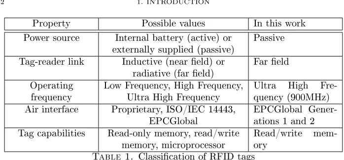
memory, microprocessor Read/write mem-ory Table 1. Classication of RFID tags
medium. The reader generates a powerful electromagnetic eld around itself and the tag responds to this eld. In passive systems, such as the one attacked in this work, placing a tag inside the reader's eld (commonly referred to as illuminating the tag) also provides it with the power it needs to operate. As stated before, the tag is usually attached to a physical object while the reader is connected to a powerful computer or to the network. A reader may, in general, communicate with many tags simultaneously.
1.1.2. A Taxonomy of RFID Systems. RFID tags can be classied ac-cording to a variety of parameters, as summarized in Table 1 on page 12. Some tags are active, containing an internal battery to provide them with power. Most are passive, relying on the reader to provide them with operating power through the eld it generates. Some tags rely on inductive coupling to link to the reader. These tags are identied by coil-shaped antennas and have a very short operating range (usually a few centimeters, depending on the frequency). Other tags use radiative coupling (also known as electromagnetic coupling) and are identied by dipole antennas, shaped more or less like a straight line. Radiatively-coupled tags typically have a longer operating range of several meters, with some types of active tags achieving ranges of 100 meters or more.
1.1. THE RFID TAG THE WORLD'S SIMPLEST COMPUTER 13
Radiatively-coupled tags oer a higher read range than inductively-coupled tags for the same reader power. This is because magnetic eld strength decreases in proportion tor3while electromagnetic eld strength decreases in proportion to
r2[55, p. 43]. In addition, while electromagnetic connections have no absolute bound on their range, magnetic induction simply does not work unless the mag-netic eld lines of the tag and coil intersect, which bounds the distance by c
2πf (according to [55], about 3.6 meters for standard 13.56 MHz tags). On the other hand, inductively-powered passive tags enjoy a relatively abundant power supply, while radiatively-powered tags are expected to work with less than one milliwatt of power (see Subsection 3.1.1.3).
Tags and readers communicate using a standard air interface protocol. Some vendors have a proprietary air interface which is supported only by their own hard-ware. Others comply to international standards. The main standard for high frequency tags is ISO/IEC 14443 [13], while the main standard for ultra-high-frequency tags is the EPCGlobal standard suite[5, 19]. The EPCGlobal air in-terface has gone through two generations of standards, both of which are covered in this work.
Finally, there are dierent capabilities for dierent tags. The simplest tag is a 1-bit tag, which merely announces its presence when illuminated by a reader. These tags are actually quite common and are used in theft prevention scenarios. The tags covered in this work are slightly more advanced, containing several hundred bits of read/write memory and a simple protocol to control them. At the top end of the spectrum there exist tags with full-edged microprocessors. These tags are in many cases standard smart cards with an added contactless interface. Due to their relatively high power requirements, contactless smart cards are usually designed for inductive coupling.
Our work focuses on passive UHF tags adhering to the EPCGlobal standard. These tags are commonly called Electronic Product Code (EPC) tags. These tags are passive and are radiatively coupled. They work in the UHF band (900MHz) and contain a small amount of read/write memory. EPC tags were designed as part of a global initiative to replace the common optical bar codes found on mar-keted goods with an RF-based electronic version. The EPC system also describes a wide-ranging technical and business-oriented infrastructure that supports this transition[18]. EPC tags improve on optical barcodes by oering an increased read range and more reliable data transfer, but more signicantly by expanding the name space for product codes from the existing 47 bits1 to 96 bits or even more. This larger name space can allow items to be tracked according to their individual identity, not only according to the class of product they belong to.
14 1. INTRODUCTION
The economics of the EPC system were designed with the notion of tags 5 costing cents apiece. As of late 2006, vendors are beginning to reach this price point for large volume purchases. A single tag is much more expensive we spent nearly $3 per tag for the ones used in our experiments. An EPC reader usually costs between $500 and $800, including antenna.
1.1.3. The Case for Security in RFID Present and Future. One may assume that the current crop of EPC tags seems too simple to protect after all, they are merely an upgrade to the optical bar code, which obviously has no security measures. The authors of [46] challenge this assumption, noting that the increased reading range of a tag, combined with the increased name space, severely compromise the privacy of individuals bearing tagged goods. This risk stems from the fact that an individual can be implicitly tracked by the specic ensemble of items he is carrying on his person. We present a more detailed survey of the security risks of RFID tags in Section 2.4. Making the data stored on RFID tags secure and trustworthy is an important concern for today's users of RFID.
In the future, the continued growth and development of the eld of pervasive computing is expected to further enhance the capabilities of RFID tags as well as their popularity and their extent of deployment. Aided by the inevitable phenome-non of feature creep, future tags can be expected to contain more sensitive data and may also have the ability to make crucial decisions based on this data. As the capa-bilities of RFID tags approach those of smart cards, the need for cryptographically enhanced security and privacy will become even more apparent.
1.2. Side-Channel Cryptanalysis
Cryptanalysts try to devise methods for attacking secure systems. There are two main approaches to cryptanalysis mathematical cryptanalysis and side-channel cryptanalysis. The dierence between the two will be explained below.
1.2. SIDE-CHANNEL CRYPTANALYSIS 15
Dynamic short circuit when transistor logic
switches states
Parasitic capacitance when long interconnects switch states
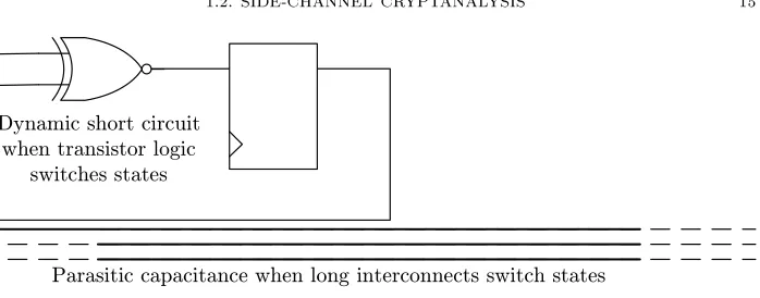
Figure 1.2. Sources of dynamic changes in power consumption in CMOS circuits
In addition to their ocial outputs, most secure systems also provide auxiliary, or side-channel, outputs as they work. Referring to the previous example, the signature server may take a dierent amount of time to sign dierent messages; the padlock may emit a series of clicks and whirrs as the dial is turned. Armed with knowledge of the internal workings of the device under attack acquired by use of inside information, by reverse engineering or simply by educated guessing cryptanalysts can now nd correlations between the secret information encapsulated by the system and these side-channel outputs. Side-channel cryptanalysis focuses on nding ways of compromising secure systems based on these correlations. Turning again to our examples, the timing information of an SSL server was used by [4] to recover its 1024-bit private key in two hours, while [3] shows how many standard safes can be cracked by observing the amount of mechanical resistance the safe dial oers as the attacker spins it.
1.2.1. Power Analysis. One very eective method of side-channel cryptanal-ysis is called power analcryptanal-ysis. Power analcryptanal-ysis focuses on relating changes of power consumption to changes in the internal state of a cryptosystem.
Before we explain the method of operation of power analysis attacks, we will briey review the internal structure of Complementary Metal Oxide Semiconductor (CMOS) circuits, the technology used to fabricate most low-power devices on the market today. A CMOS integrated circuit (IC) consists of internal state registers, some logic circuitry that makes use of these registers, and an interface that connects these functions to the outside world. Both state and logic are implemented by networks of transistors or gate elements (GEs). The gate elements are connected by interconnects, which are strips of metal running through the integrated circuit. More complex systems (beyond the scope of this work) may also use dynamic random access memory (DRAM) to store their state.
16 1. INTRODUCTION
circuit current and loading capacitance current. The leakage current is a constant dissipation which is a result of the manufacturing process of CMOS and is not inuenced by the internal state of the tag. The other two contributors are dynamic: The direct-path short circuit current is a rush of current that occurs whenever transitions in the CMOS logic result in a temporary short circuit between the IC's power supply and the ground; The loading capacitance current results from the fact that a circuit's interconnects behave like capacitors and thus require a charge/discharge current when they change state. According to [1], about 15% of the dynamic power consumption of typical devices results from dynamic short circuits, while 85% is the result of parasitic loading capacitance. Both dynamic sources of power consumption manifest themselves only when state bits in the IC ip their values.
These dynamic properties mean that, in general, a active CMOS device con-sumes more power than an idle device, allowing an attacker to learn exactly how long certain operations take and raising the possibility of timing-based side chan-nel attacks. With suciently sensitive equipment, an attacker can also estimate how many individual bits ip at every point of time, allowing even more powerful attacks. To mount a power analysis attack, the attacker places a sensitive current probe between the device and its power supply, then measures the change in power consumption over time. This attack is especially suited to smart cards, a popular class of secure devices which is designed to be tamper resistant but still has its power supplied by an outside party.
A more detailed survey of power analysis attacks and the work done to prevent them is available in [1] and in [28].
1.2.2. Protection from Side-Channel Attacks. As mentioned previously, side-channel attacks gain their strength from the correlations between a system's secret data and its side-channel outputs. Side-channel countermeasures are gen-erally designed to minimize this correlation. There are several approaches toward this goal, including masking the secret with some random data, attenuating the side channel by some form of shielding and using specially designed components with less side-channel leakage. We survey several countermeasures suitable against power analysis attacks in Section 5.2.
1.3. Our Contribution
1.4. STRUCTURE OF THIS DOCUMENT 17
attack by recovering the kill password of an EPC tag. We also present an existing power analysis countermeasure which ts into the tag manufacturing process and eectively protects against our attack.
1.4. Structure of this Document
CHAPTER 2
Previous Work
This section will discuss previous work related to our results.
2.1. Password Guessing Attacks
The results presented in this work make use of power analysis to try and guess a password. Using the fact that we can guess the password one bit at a time, the time required to search the password space is reduced from exponential to linear, and thus it is easy to attack arbitrarily long passwords. The rst documented use of this attack as a way of guessing passwords in a computing environment was in the TENEX operating system, circa 1970 [32, Section 2.1].
2.2. Power Analysis of Smart Cards and Other Cryptosystems
The capabilities of power analytic attacks were rst demonstrated in an aca-demic setting in [28]. Power-analysis attacks lend themselves naturally to smart cards, since the internal state of smart cards is protected from outside inspection by various tamper-proong methods while their power supply is run from an external line and, as such, can be delicately monitored by an attacker without tripping the tamper protection. There have been many follow-up works to [28], exploring both the capabilities of power analysis and the cost involved in preventing them. Power analysis has been used to extract the keys from smart cards using secret key ciphers such as DES [15] and AES [14], as well as devices using public key cryptosystems such as RSA [37]. In [46] the authors suggested that RFID tags may be vulnerable to power analysis and fault attacks. In [42] the authors presented an RF front-end for an inductively coupled contactless smart card, remarking that Contactless smartcards are especially susceptible to power analysis because the power signature of a transaction is actually broadcast in the air.
2.3. Remote EM-based Attacks
Several other research works present attacks mounted by a remote attacker armed with a directional antenna. Two interesting results are discussed below.
20 2. PREVIOUS WORK
2.3.1. Screen Sning. Cathode ray tube (CRT) displays operate by scan-ning a single electron beam of variable intensity over the entire screen in a predeter-mined pattern of lines. The signal controlling this intensity is called the luminance signal. This luminance signal is subjected to a very high level of amplication be-fore it is used to manipulate the strength of the electron beam. In [54] Wim van Eck demonstrated that this signal leaks out of the display unit in the form of elec-tromagnetic radiation. This signal can be then intercepted and used to reconstruct the image shown on the display. In a demonstration for the BBC's Tomorrow's World show in 1985, van Eck used a van-mounted VHF antenna to intercept the screens of computers in the Scotland Yard building several tens of meters away from the attacker.
In [31], this attack was further extended to modern LCD displays. The attacks of [31] operates in frequency ranges and signal envelopes similar to the ones used in our attack, and thus his estimates on the usable attack range were useful to us as well.
2.3.2. Smart card Emanations. Since any conducting wire inside a com-puting device can be considered as a transmitting antenna, several researchers have attempted to monitor the electromagnetic emanations of the internal circuits of a smart card and thus deduce its internal state without tripping the tamper-protection safeguards. These attacks are usually carried out by placing a short coil antenna directly above the smart card, exactly over some location of inter-est. In [36], the authors demonstrated a dierent remote attack on cryptographic smart cards using electromagnetic emanations. In this attack the receive antenna was not located directly above a specic spot on the smart card, but rather at a distance of 2 meters from the card. The attack was performed in an anechoic chamber - a special environment designed to minimize the interference caused by external radio frequency sources and by multipath propagation of the intercepted signal. Our attack is dierent than the attack in [36] in that it does not monitor the electromagnetic emanations of the circuits inside the device under attack, but rather presents an indirect way of monitoring its actual power consumption. Our method of attack apparently has better range and more resistance to noise than the attack in [36], since we were able to mount it in an electromagnetically noisy lab environment and without explicity ltering against multipath eects.
2.4. ATTACKS ON RFID TAGS 21
still be relevant data in the power consumption of specic parts of the device). On the other hand, surrounding the chip at the heart of the tag with EM shielding (without, of course, shielding the antenna) will protect against standard EM-based attacks but will not protect against our attack.
2.4. Attacks on RFID Tags
2.4.1. The RFID Threat Model. The current lines of attack against RFID tags are derived from the capabilities of today's tags. At present, the most common functionality of a tag is to provide a static payload (identifying the item to which it is associated) to the reader. Either reader or tag may be required to authenticate themselves, and the signal exchanged between reader and tag may be encrypted. In this scenario, an RFID adversary may desire either to prevent the tag and the reader from communicating, to masquerade as the tag or as the reader, or to bypass the channel encryption. The general threat model is surveyed in detail in [46]. One specic threat which we address in this work is the case of an adversary disabling or rewriting tags at will.
Generally speaking, the technological situation is bringing RFID tags ever closer to having all properties of a standard recongurable computer, both in terms of the quantity and quality of the information it may store and in terms of its computing power. The threat model will obviously evolve as the capabilities of RFID tags grow, nally converging into the standard threat model for a personal computer.
2.4.2. Current Attacks on RFID Tags. This section presents a short sur-vey of some attacks against the current line of passive RFID tags. Since this work focuses on physical layer attacks, we will present three works in which tags were attacked at the physical layer zapping, jamming and skimming.
Zapping attacks attempt to incapacitate a single tag, rendering it unable to communicate with any reader. An attacker with physical access to the tag can achieve this goal by cutting the antenna apart using a pair of scissors the stubs of the antenna which remain connected to the tag will provide it with much less power than a full-sized antenna, dramatically reducing its read range[23]. A more advanced attacker can try and create an electromagnetic pulse (EMP) which will overwhelm the tag's reciever circuit and render it unusable. In [39] the authors show how to create an EMP gun using a disposable camera's ash circuitry and demonstrate its use in disabling ISO/IEC 14443 RFID tags. The authors also note that their EMP gun has the same destructive eect on personal computers, portable music players and pacemakers.
22 2. PREVIOUS WORK
special tag designed to prevent any other tags being read in its vicinity. The blocker tag is designed to participate in the EPC singulation protocol (see [5, subsection 4.2.2]) and to answer positively to all reader inventory queries, in fact creating the false impression that all296possible tags are present in the reader's vicinity. Since the blocker tag understands the EPC protocol, it can be designed to have a more benevolent behaviour, perhaps blocking only a certain subset of the ID space (for example only medicines) or disabling itself when being presented with a properly authenticated reader. While this attack works in the application layer, another attack, presented in [17], achieves similar functionality at the physical layer. The attack of [17] prevents tags from even hearing the reader by creating a competing signal in the same frequency range as the reader. This attack is made easier by the fact that while the RFID reader performs frequency hopping to help it share the air with other devices, the RFID tag listens undiscriminately to all signals in its range.
CHAPTER 3
Theoretical Background
This section will describe the theoretical aspects of our work. It will describe the family of tags we attack, and how we intended to attack them.
3.1. The EPC Standard Family
The RFID system we considered was the EPC system, used in tags attached to items of merchandise in retail and other supply-chain scenarios. The standards body governing the concepts of this system is EPCGlobal, a not-for-prot organization formed around MIT's Auto-ID Center in 2003[18].
The EPC standards dene the capabilities of the tag and reader and determine how the two should communicate. The communications protocol consists of two layers:
• The physical layer (also called the air interface) denes the radio char-acteristics of the protocol, including the way bits and symbols are repre-sented and the allowed frequencies and power levels used by the reader. • The application layer denes the set of commands the reader and tag
should exchange. It also denes how the tag should respond to the com-mands it receives.
The EPCGlobal architecture denes in [45] 6 classes of tags, ranging from Class 0 to Class 5. Class 0 tags are the weakest they are read-only devices capable only of emitting a certain xed ID they were assigned when they were manufactured. Class 5 tags are the most powerful, being for all practical issues full-edged portable computers with support for the EPC air interface. The most common tag class, and the one discussed here, is the Class 1 tag. It denes a passively-powered tag with no computational resources other than a small amount of read/write memory and the logic required to access this memory.
The Class 1 EPC protocol went through two generations. The rst generation was dened by MIT's Auto-ID center in [5]. While it was never formally ratied, the Generation 1 protocol was accepted by the industry and was deployed in hun-dreds of millions by late 2005 [9]. The parts of the protocol which were vague or incompletely specied were implemented arbitrarily by manufacturers, leading to
24 3. THEORETICAL BACKGROUND
Antenna
Power Supply
Demodulator
Modulator
Control Logic
EEPROM Power
Extraction
Received Data
Read/ Write Transmitted
Data
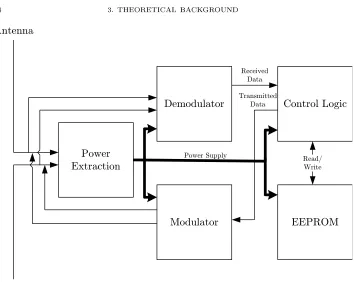
Figure 3.1. The general structure of a tag
some incompatibility problems and to the emergence of a de-facto standard based on imitation of the leading vendors' implementations (see for example [50]).
The current recommended standard is called Class 1, Generation 2 (C1G2), and is dened in [19]. While both generations of the Class 1 protocol share a common air interface, their application layer is quite dierent1.
We will now discuss the parts of both protocol layers which are relevant to our attack.
3.1.1. The Physical Layer. The aspects of the physical layer we will discuss are the frequencies and power level used, how power is supplied to the tag, and how tag and reader communicate.
3.1.1.1. The General Structure of a Tag. Figure 3.1 on page 24 shows the gen-eral structure of a passive UHF tag, as described in [24].
The tag's antenna is its link to the outside world. The signal incident on the antenna contains both the power required to operate the tag and commands from the reader. The power extraction circuit converts the low-amplitude AC input to a 5V DC voltage which is provided to all other modules. The demodulator, or decoder,
1The common air interface was chosen to allow Generation 1 readers to support Generation 2
3.1. THE EPC STANDARD FAMILY 25
extracts the data from the incoming signal and forwards it to the control logic. The control logic module, which is in charge of implementing the tag's command set, is generally constructed of a nite state machine that has access to electrically erasable and programmable memory (EEPROM). The EEPROM is used by the tag to store long-term, non-volatile data such as the tag's ID. The modulator is used to convey responses from the tag back to the reader. This is done by dynamicaly changing the impedance of the tag and thus the magnitude or the phase of the signal it reects back to the reader's receive antenna (see Subsection 3.1.1.5). Recalling our cryptanalytic intentions, it is apparent that while all six modules mentioned above have an eect on the transient power consumption of a tag, the secret information we are after is contained only in the power consumption of the control logic, the EEPROM, and the bus connecting the two.
3.1.1.2. Frequencies and Power Levels. The EPC system operates in the industrial-scientic-medical (ISM) frequency band. The ISM band is unique in the sense that low-powered transmitters can be used in it without being individually registered and licenced. The exact choice of frequency for the ISM band varies between coun-tries, but it is generally between 860 and 960MHz.
In a passive RFID system, the electromagnetic eld generated by the reader is used to power the tags it interrogates. The amount of power available for the tags decays quadratically as the distance between the tag and the reader grows, and all tags require a certain minimal amount of power to operate. Thus, for any xed tag design, the maximum transmit power a reader can use immediately determines its maximum range.
The dierent national standards institutes dene the maximum power allowed for an RFID reader. As shown in [12, subsection 4.2.5.2], this maximum power limit is commonly measured using the eective isotropic radiated power (EIRP) rating. EIRP is dened in [11] as the power that would have been radiated by an isotropic antenna with the same power density as the real antenna in the direction of maximum gain.
Practical antennas do not have a uniform power distribution in space, but rather follow some radiation pattern. For example, a dipole antenna generates a strong eld on the plane normal to its axis and incident on its center, while it radiates no power along the axis of the dipole itself. The EIRP measurement method means that users cannot try to increase the range of their readers while staying within the regulated power constraints by using a high-gain, highly directional antenna2. Figure 3.2 on page 26 shows the radiation patterns of several types of antennas, 2A passive tag's radiated eld is always much weaker than the reader's eld. However, the tag's
26 3. THEORETICAL BACKGROUND
EZNEC Demo
Dipole in free space
NBS Yagi (ANT. BOOK p. 18-7)
Radiation pattern of a dipole antenna
Radiation pattern of a Yagi directional antenna Radiation pattern of a
theoretical omnidirectional antenna
Figure 3.2. The radiation patterns of dierent types of antennas
plotted using EZNEC [33]. The contour line in the gure represents areas in space with similar power density.
The exact denition of the allowed frequencies and power levels for EPC tags varies between countries. In the USA the Federal Communications Commission (FCC) denes a frequency range of 902928MHz and a maximum EIRP of 4W. In most of Europe the European Telecommunications Standards Institute (ETSI) denes a frequency range of 865.6867.6MHz and a maximum EIRP of 3.2W[2]. As of late 2006, RFID regulation in Israel was still a work in progress the suppliers we contacted stocked both FCC and ETSI-compliant tags.
EPC tags transmit their responses to the reader by modeulated reection of the reader's signal. Due to this property, the operating frequency of a tag-reader system is completely determined by the reader. Thus, a single tag can be made to be both FCC- and ETSI-compliant.3 In general, a tag operated outside its recommended frequency range will still work, but its usable read range will be dramatically lower. 3.1.1.3. Power Supply to Passive Tags. The carrier wave generated by the reader is used both to provide the tag with power and to send it data. While this subsection will focus on power extraction, the next subsection will deal with the data payload carried by the reader's signal.
According to Maxwell's equations, placing a conducting antenna in a variable electromagnetic eld causes a current to ow through the antenna. Conversely, passing an alternating current through a conducting antenna generates an electro-magnetic eld around it. In standard applications of radio-frequency data transfer, such as FM radio, the signal induced on the antenna by the external electromagnetic
3Tag vendors may have an incentive to create tags which are not usable throughout the world.
3.1. THE EPC STANDARD FAMILY 27
eld provides the data signal (for example, the music on the radio), while power is provided by another source. Passive tags, on the other hand, have the ability to extract their operating power from the current induced on their antennas.
The reader powers the tag by generating a sine wave with the approximate fre-quency of 900 MHz. If the tag antenna is properly matched to this signal, a standing wave will develop on the tag's antenna. This standing wave is an alternating voltage dierential which causes current to ow through the tag circuitry.
As stated in Subsection 3.1.1.2, real-world antennas are not isotropic, meaning that their orientation in space has an eect on the power of the signal they receive. Tag makers are usually interested in maximizing the tag's usability, regardless of its orientation, so tags usually use half-wave dipole antennas, which are relatively omnidirectional. These antennas are constructed from a straight segment of con-ducting material with a length equal to half the wavelength of the signal (in our case approximately 15cm). Vendors usually meander the antenna in a somewhat curved pattern to minimize the eect of the dipole's blind spots directly along the antenna's axis.
To maximize the transfer of energy from the antenna to the IC, the tag's internal circuits are designed to expose a purely resistive load toward the antenna. This is done by cancelling out any capacitive or inductive loads generated by the tag's internal circuitry by an additional network of coils or capacitors.
We can now use the standard microwave engineering equations to discover the power available to the tag.
To see the total power available to the tag circuit's power extraction module, we can measure the proportion of the sphere of energy surrounding the reader which is captured by the tag antenna's eective area. This gives us the formula
(1) PTag=PReader· ATag
4πr2
The eective area is a measure which depends on the antenna's geometry and the incident wavelength. For a tag with a half-wave dipole the eective area is dened in [12] as λ2
2π. Assuming a 900MHz signal, for whichλ= c
9·106 = 33.31cm, we arrive
atATag ≈88.3cm2. Assuming a tag located 3 meters away from an ETSI-compliant reader with an isotropic antenna transmitting at 3.2W, the total amount of power available to the tag is approximately250µW.
This power is presented to the tag as a standing waveU0generated on the tag's antenna. According to [12, p. 125], the amplitude of this standing wave is dened as
28 3. THEORETICAL BACKGROUND
where `0 is the eective length of the tag's antenna and E is the electric eld strength of the incoming wave. The eective length is a function of the antenna's eective surface areaATag, of the wireless medium's characteristic wave impedance
ZF and of the antenna's radiation resistanceRR. The strength of the electric eld is a function of the reader's eective isotropic transmitted power and of its distance from the tag:
`0= 2
r
ATag·RRad
πZF , E=
r
PReader·ZF
4πr2 Combining the two equations we obtain
U0=
r
ATag·RRad·PReader
π2r2
For a standard half-wave dipole antenna RRad ≈ 73Ω[12]. Assuming that
ATag ≈88.3cm2, we arrive at the nal approximation of0.258
√
PReader
r Volts. Re-turnimg to the previous example, the tag described there can expect a voltage dierential of about 0.15 Volts.
To reduce costs of tags and enable high-volume manufacturing, tag circuitry is usually constructed from older-generation CMOS silicon, which requires a 5V DC operating voltage. To convert the low-voltage AC signal received on the antenna to a reasonable DC source, the tag makes use of a circuit called a charge pump. As shown in [24], this circuit recties and amplies the standing wave into a higher-amplitude DC voltage and nally uses it to charge a capacitor that powers the rest of the circuit. The power extraction process is inherently lossy, meaning that typically only 15% of the power incident on the tag's antenna will actually be available to power the tag's internal circuitry (see [24, subsection V]).
3.1.1.4. Data Transfer from Reader to Tag. The EPC protocol is based on a reader-talks-rst methodology, in which the tag may only transmit data as a direct response to reader queries. The communication protocol is half-duplex: at any stage in time only one of the two devices may transmit data.
In both generations of the EPC protocol the reader sends the tag commands in the form of packets, each of which consists of a sequence of symbols. Each symbol consists of a series of binary bits. The symbols have variable lengths, generally consisting of 2 to 8 bits. The dierent lengths for each symbol form a basic Human encoding that allows common commands to be sent and handled more eciently. Each bit is sent by varying the strength of the reader's eld between two levels over time, using a scheme called pulse amplitude modulation (PAM) or amplitude shift keying (ASK)4. The changes between the high and low levels are not abrupt in practice. Instead, the output signal is low-pass ltered, resulting in a gradual
4The Generation 2 standard oers two additional modulation methods, SSB-ASK and PR-ASK,
3.1. THE EPC STANDARD FAMILY 29
Bit is decoded
here Generation 1 Symbols
T0/8
T0
T0*3/8
T0
TARI*1.75
PW
TARI
PW “0” bit:
“1” bit:
Generation 2 Symbols
“0” bit:
“1” bit:
Figure 3.3. Bit shapes of Generation 1 and Generation 2 symbols
change in power levels. This ensures a narrow reader bandwidth, which is required by regulations.
Both generations of the EPC protocol use similar bit shapes, as shown in Figure 3.3 on page 29 (see [5, subsection 5.3] and [19, subsection 6.3.1.2.3]):
The values of the parameters T ARI, T0 and P W used in the diagram are dened by the protocol and can very between dierent regulatory domains. Note that in both protocols the value of the bit can be measured by calculating the distance between a rising edge and the following falling edge. Thus, actions that must be carried out once per bit are probably performed as soon as the falling edge is detected by the tag.
30 3. THEORETICAL BACKGROUND
symbols which have a relatively high duty cycle. In fact, Generation 2 high-powered operations that write to the EEPROM (tag write and tag kill) require that the reader provide the tag with a long stretch of unmodulated carrier wave (CW) while the command executes (see [19, subsections 6.3.2.10.3.3 and 6.3.2.10.3.4]). This CW sequence oers the highest amount of possible power to the tag, ensuring these two power-hungry commands will execute completely.
The protocol allows some variability in two parameters of the shape of indi-vidual bits the symbol length and the depth of modulation. A shorter symbol length allows a faster symbol rate but increases the bandwidth of the reader signal. A deeper modulation increases the dierence between high and low power levels, increasing the reliability of the tag's demodulator and thus allowing an increased range, but again at the price of a higher-bandwidth signal. In general the FCC al-lows shorter symbols with deeper modulation to maximize speed and range, while ETSI uses longer and shallower symbols to minimize the eect of the EPC system on other ISM band users (see [5, subsection 5.3.1]).
As stated in the previous section, the tag is powered by the reader's signal. Since this form of modulation causes the amplitude of the reader's signal to vary in time, the power extraction module of the tag uses an intermediate power storage in the form of a large capacitor. Generally speaking, the capacitor is charged during periods in which the reader's signal is at its high level, providing power to the rest of the tag's circuit while the reader's signal is relatively weak.
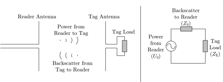
3.1.1.5. Data Transfer from Tag to Reader. Upon receiving a command from the reader, the tag can send a response to the reader using the backscatter modu-lation principle. As noted in Subsection 3.1.1.3, any current owing through the tag's antenna immediately causes an electromagnetic wave to be generated around it. By controlling the current owing through the antenna, the reected eld can be modulated and thus used to convey meaningful information to the reader.
Assuming a xed input voltage on the tag's antenna terminals, the tag can control the current owing through the antenna by changing the impedance exposed to the antenna by the tag's internal circuitry. Changing the resistance of the tag's internal circuit has an eect on the amplitude of the reected eld. Changing the reactance of the circuit has an eect on the phase of the reection. As demonstrated in [24, subsection 3.B], the tag can switch rapidly between two impedances and thus modulate its response to the reader. To switch between the two impedance values, the tag uses transistors to connect or diconnect an additional subcircuit consisting of a capacitor (for changing phase) or a resistor (For changing amplitude) in parallel to the other tag functions.
3.1. THE EPC STANDARD FAMILY 31
Power from Reader to Tag
Backscatter from Tag to Reader
Tag Antenna
Tag Load Reader Antenna
Power from Reader
(U0)
Tag Load
(ZE) Backscatter
to Reader (ZS)
Figure 3.4. The reader-tag channel and its equivalent circuit
regardless of whether the tag is transmitting a '1' bit or a '0' bit (see [24, subsection IV.B]). In practice, this form of phase modulation can also be detected by an AM receiver at the reader because the phase dierences cause interference (either de-structive or conde-structive) with the reader's transmitted signal, resulting in dierent amplitudes for dierent phase dierences. Because the intereference can be either destructive or constructive depending on the relative positions of the tag and the reader, the tag cannot tell beforehand whether reecting a stronger signal will make the reader's received signal weaker or stronger. To get aronud this obstacle, the tag modulates the response data into the timing of the changes between high and low states, not into the high or low values themselves. This is actually a basic form of frequency modulation, commonly known as frequency shift keying (or FSK). From this point we will focus on changes of amplitude due to a varying resistive load, since this eect is more relevant to the attack we present.
32 3. THEORETICAL BACKGROUND
The relation between PE and PS (the power consumption of RE and RS, re-spectively) is calculated using the standard voltage divider equation:
PS(t) = I(t)2RS=
U
0
RS+RE(t)
2
·RS (3)
PE(t) = I(t)2RE(t) =
U
0
RS+RE(t)
2
·RE(t)
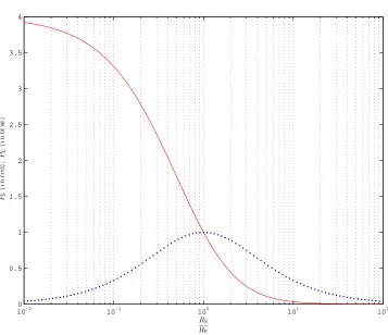
U0is determined by the strength and wavelength of the reader's eld and by the properties of the tag's antenna and is independent of the tag's power consumption. A plot of the relation between the internal resistanceRE, the absorbed power PE and the reected power PS is shown in Figure 3.5 on page 33. The graph
is normalized such that PS = PE = 1 when RS = RE. We can make several
observations on this graph. First, the absorbed and reected power do not sum to a constant along the graph. This counterintuitive result stems from the fact that some power is transmitted through the tag without being absorbed or reected. Two interesting end-cases for this relation are whenRE= 0(short-circuit), in which the received signal is completely reected, and whenRE→ ∞(open circuit), in which it is completely transmitted. In both of these situations zero power is available for the tag's internal circuitry. The maximum eective power available to the tag is found whenRS=RE, indicating the power extraction can never reach an eciency of more than 50%.
This detail of the EPC protocol is actually quite signicant in our attack the backscatter modulation method, used by the tag to send data to the reader, is also how power consumption data is leaked to the adversary. To get a taste of this eect, assume that the tag's resistance at the idle state is equal to RS. A
momentary power draw caused by a transition in the control circuitry causes the tag's eective resistance to lower momentarily. Turning again to Figure 3.5 on page 33, we can see this will cause the tag's working point to move left on the graph, resulting in a momentary surge in the amount of reected power.
3.1.2. The Application Layer. The two generations of EPC protocols dene many commands which can be exchanged between tag and reader. Most of them are outside the scope of this work. We will survey two interesting areas of functionality the tag singulation protocol and the kill command. More commands are described in [5] and [19].
3.1. THE EPC STANDARD FAMILY 33
10−2 10−1 100 101 102
0 0.5 1 1.5 2 2.5 3 3.5 4
RS
RE
PS
(i
n
re
d)
,
PE
(i
n
bl
ue
)
Figure 3.5. The relation between internal resistance and reected power, based on [12, p. 124].
3.1.2.1. Tag Singulation. Radio is inherently a broadcast medium. At any time the radio environment may contain many devices, all sharing the same wireless channel. This is especially the case when considering the primary application of EPC tags in supply chain management (supermarkets and warehouses), in which hundreds of tags may be present simultaneously in the eld of one or more readers. The singulation protocol is designed to allow the reader to select a single tag and communicate with it exclusively5. There are dierent singulation protocols for Generation 1 and Generation 2 tags.
The Generation 1 singulation protocol is dened in [5, subsection 4.2.2]. The result of a successful Generation 1 singulation is usually the tag's 96-bit payload. The payload also serves as the unique address of commands sent to the tag. There are three variants of the singulation protocol, designed to address dierent pop-ulation densities and security concerns (see [46]). Assuming the tag's payload is
5While both generations of the protocol also oer commands that address targeted groups of tags
34 3. THEORETICAL BACKGROUND
known beforehand, it is not generally necessary to perform singulation against a Generation 1 tag.
The Generation 2 singulation protocol is dened in [19, subsection 6.3.2.10.1]. As opposed to the Generation 1 protocol, the end result of a Generation 2 singula-tion is always a 16-bit random handle and not the tag's payload. This identier is generated afresh each time the tag is powered up, so a Generation 2 tag may not participate in most commands unless the reader explicitly performs singulation to discover the tag's random identier.
3.1.2.2. The Kill Command. The kill command is designed to irrevocably dis-able a tag and render it unusdis-able. This kill feature was designed as a privacy benet, in response to concerns raised by various organizations. The kill function prevents the contents of the tag from being disclosed after it has left the supply chain and then being used to track the individual bearing the item.
Since the Generation 1 protocol was never formally ratied, vendors ended up misapplying the kill command's original intentions. Instead of irrevocably disabling the tag, most vendors chose instead to delete all tag data upon receipt of a kill command (see [50, p. 26]). This means that the tag still participates in protocol commands, but the ID it sends out is an all zero string. Of course, this means the bearer of the tag can still be tracked due to the existence of the blank tag on his person. The adversary can even rewrite the blank tag with a unique value and track this new value in the future.
The Generation 2 protocol strictly demands that tags be completely disabled when they receive a kill command. A dead Generation 2 tag should not respond to any command sent by the reader. In practice some tag vendors still disregard this requirement, but the brand we tested implemented it6.
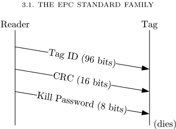
The Generation 1 kill command, as dened in [5, subsection 4.2.2] (and elabo-rated upon in [50, pp. 26]), is shown in Figure 3.6 on page 35. Both this gure and Figure 3.7 on page 36 omit for clarity several implementation-related elds, such as parity checks, message headers and preamble sequences.
An execution of the Generation 1 kill command consists of a single packet being sent from the reader. The packet species the tag's entire 96-bit payload, a checksum, then the 8 secret bits of the kill password, another checksum and nally the pattern for binary '1' repeated for 30 milliseconds. If the tag's payload matches the specied payload, the kill command is correct and the checksums match, the tag should erase all of its non-volatile memory and respond to no further commands from any reader. Otherwise, it ignores the command. In both cases, the tag is completely passive during the entire process and does not send any reply indicating the success or failure of the kill command.
3.1. THE EPC STANDARD FAMILY 35
Reader Tag
Tag ID (96 bits) CRC (16 bits) Kill Password (8 bits)
(dies)
Figure 3.6. The Generation 1 kill command
There were several problems with the Generation 1 implementation. The rst and most easily noticeable problem is the small key space with only 256 possible kill passwords, it is trivial to conduct a brute-force search for the kill password of the tag and disable it. Another more subtle problem was discussed by [46] and is related to the assymetry in signal strengths between tag and reader. Since the reader emits a very powerful signal, it is reasonable to consider a passive adversary who can listen only to reader commands, but not to tag responses. During the kill command the entire contents of the tag memory are broadcast by the reader, allowing such an adversary to learn of the dead tag's former identity from a potentially much larger distance, even beyond the detection range of the tag. Finally, we must recall that vendors implemented this kill command improperly, severely compromising its security benets.
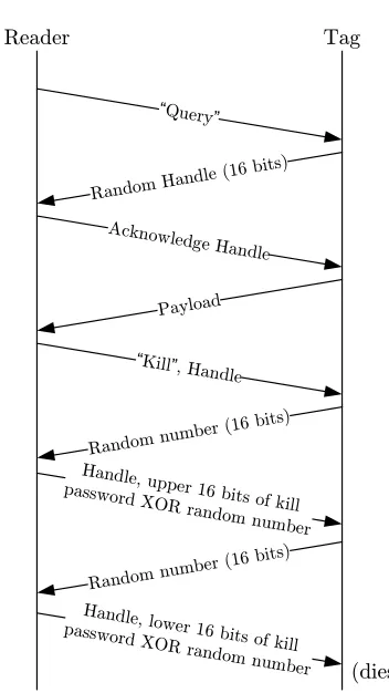
The Generation 2 kill command was designed to solve these problems. The key space was changed from 8 bits to a more adequate 32 bits, raising the time of a brute-force attack from under a second to around 8 months. The Generation 2 protocol is designed to accomodate the assymetric channel between tag and reader the reader never broadcasts incriminating data such as the tag's EPC code or the kill password itself. Finally, the protocol strictly denes that a killed tag should be honestly and truly dead, preventing tag vendors from merely clearing their tag memories.
Execution of the Generation 2 kill command is more complex than the previous generation. This is because tags must be singulated before being sent the kill command, and also because the entire 32 bits of the password are not sent in a single iteration, but rather in two. This design choice was made in order to trim 16 bits from the amount of internal storage required in the tag, since the tag has only to remember 16 bits of cover coding instead of 32, as shown below.
36 3. THEORETICAL BACKGROUND
Reader Tag
“Query”
Random Handle (16 bits)
Acknowledge Handle
(dies)
Payload
“Kill”, Handle
Random numbe
r (16 bits)
Handle, upper 16 bits of k ill password XO
R random number
Random numbe
r (16 bits)
Handle, lower 16 bits of k ill password XO
R random number
Figure 3.7. The Generation 2 kill command
First, the reader and tag perform the singulation protocol common to all Gen-eration 2 commands. The singulation protocol ends with the tag identifying itself with a 16-bit random handle. Next, the reader requests 16 random bits from the tag, and responds with the rst 16 bits of the kill password, XORed with the ran-dom bits the tag just sent. The protocol continues with the tag sending the reader an additional 16 random bits and the reader replying with the second half of the password. If all 32 bits match, the reader is expected to send a long stretch of CW which provides the tag with sucient energy to delete its long-term storage. It can be noted that the tag acknowledges each 16 bit segment in turn, but only checks for correctness after the entire 32 bits of the password have been sent. This prevents the attacker from launching a trivial form of a meet-in-the-middle attack taking216 attempts on average to brute force the two halves of the password seperately.
3.2. THE PARASITIC BACKSCATTER CHANNEL 37
transmitted request and the tag's response before it can discover the kill password, protecting against asymmetric attackers.
Careful observation will show that the tag can be designed so that it never uses much more than 48 bits of temporary storage throughout the kill protocol (16 bits for the handle, 16 for the cover coding, 16 bits for CRC calculation), and that 32 of these bits are explicit outputs of the internal 16-bit random generator and are not further manipulated. Random access memory is a very scarce resource in low-cost RFID tags, costing at least 6 gate elements per bit. Minimizing the gate count is one of the most eective tools RFID circuit designers have to minimize the cost and increase the range of their devices. This fact leads us to believe that tags do not store the entire 32 bits of the kill password in memory, but instead check the rst 16 bits and carry only a single bit of state (whether this half of the password was correct or incorrect) into the second 16 bits. This behaviour should be also observable by power analysis (although we did not have the time to run this experiment), theoretically allowing the attacker to launch a 216 time meet-in-the-middle attack.
3.2. The Parasitic Backscatter Channel
As stated in Subsection 3.1.1.5, momentary changes in the internal resistance of the tag result in changes to the strength of the tag's reected eld. This backscatter channel is used by the tag for intentional communication with the reader. We set out to examine whether we could also observe the minute changes in internal resistance which result from the internal state of the control circuits, thus enabling a power analysis attack from a distance.
3.2.1. Estimating the Power Consumption from the Reected signal. The power supplied to the tag by the reader is shared by two consumers the power reected by the tag and the power it consumes internally. Because of this fact, the reected power PS =I2RS is a function of the tag's internal power consumption
PE. Taking (3) and solving forRE, we obtain:
(4) RE(t) =U0
s
RS
PS(t)−RS
AssumingU0is known andRsis constant, (4) gives us a direct way of obtaining the power consumption of the tag by measuring its reected power.
38 3. THEORETICAL BACKGROUND
K
2V
R
(t)
Tag
Reader
Adversary
V
R(t)
K
1V
T(t)
Figure 3.8. The multiple sources of the adversary's trace
reader and may contain noise or undesirable artifacts. Finally, it assumes we can accurately measure the power reected from the tag in the presence of the much stronger signal generated by the reader itself. As we will see, these simplications do not prevent our attack.
3.2.2. Methods of Attack. All of our attacks had a common structure. Us-ing a cooperatUs-ing reader, we sent a series of kill commands with incorrect passwords to the tag under attack. We then measured the power reected over time from the tag, taking care to minimize the eect of the reader on our measurements. Taking several such traces and comparing them, we tried to measure the eects of dierent password values on the shapes of the traces.
While the signal reected from the tag has a strong dependence on the tag's power consumption, it also has other external inuences which are not found in con-ventional power analysis traces. To show this fact, let us derive a simple expression for the reader signalvR(t), as incident on the tag's antenna:
(5) vR(t) =aR(t) cos (2πfct+ϕ) +n(t)
In this equation the reader signal vR(t) is a sinusoid with carrier frequency
3.2. THE PARASITIC BACKSCATTER CHANNEL 39
tag with commands and with their parameters. While (5) should also include some path losses due to the distance between the tag and the reader, we chose to absorb them intoaR(t).
This received signal is backscattered by the tag with a varying reection coe-cient determined by the tag's power consumption, as dicussed in Subsection 3.2.1:
(6) vT(t) =KaT(t)vR(t) +nT(t) =KaT(t)aR(t) cos (2πfct+ϕ) +n(t)
Finally, this signal is received on the attacker's antenna combined with the reader's signal:
(7) vA(t) =K1vT(t+ϕ1) +K2vR(t+ϕ2)
Where the phase dierences stem from the dierent distances the reader and tag signal have to travel before they reach the attacker. While there may be some additional data encoded in the phases, our AM receiver was not designed to make use of them, so we ignore them from this point on. Substituting (6) into (7), we see that the intercepted signal is actually an amplitude-modulated version of the reader's signal, which is itself amplitude modulated:
(8) vA(t)≈K3 K4+aT(t)aR(t) cos (2πfct+ϕ) +n(t)
We can now pass this signal through our AM demodulator to receive our amplitude trace:
(9) T(t)≈K3 K4+aT(t)
aR(t)
The value ofaT(t), which is somewhere inside the above equation, is functionally equivalent to the traces provided as an input to conventional power analysis attacks, and our goal is to extract it.
Let us rst examine a reader which is transmitting a sinusoid of constant ampli-tude aR≡const
. This mode of transmission is called carrier wave, or CW, in the EPC specications. In the case of a reader transmitting a CW signal a wideband AM receiver tuned tofc would be enough to extract the value ofaT(t)and send us on to the power analysis part. A long stretch of CW, however, is rarely found in the attack-worthy parts of current protocol implementations7.
We are forced, then, to nd a practically plausible way of extracting the tag-contributed signalaT(t)from the above signal. We are fortunate in the fact that, compared toaT(t), the reader signal aR(t)is both slower-varying and more pre-dictable. Several approaches to extracting aT(t) from the combined trace are
7One can argue that in the case of a processing-intensive task, such as an AES encryption or a
40 3. THEORETICAL BACKGROUND
Troughs – tag performs
calculations
Pulses – tag charges up
Direct observation
Pulse power measurement
Figure 3.9. The attack methods compared
presented below, as well as advanced approaches we did not have the resources to try.
3.2.3. The Direct Observation Attack. In this attack we attempted to directly capturevA(t)and then analyze it oine. Our wideband reciever performed AM demodulation for us, leaving us with a trace of the form K+aT(t)a
R(t). The main problem with this attack is an instrumentation problem the in-tercepted signal has a very large amplitude range, most of which is caused by the uctuations in the reader signalaR(t), while modern digital oscilloscopes only have about 1% accuracy in the vertical scale. This means that we had to choose between capturing the whole gamut with a high measurement noise or limiting the measure-ment to parts of the vertical scale and risk losing meaningful data. As we will see later, for our attack it suced to look only at the tops of the peaks of the original signal.
3.2.4. The (Theoretical) Dierential Observation Attack. The instru-mentation problem encountered in the direct observation attack could be solved if we could somehow cancel out the eect of aR(t) on the trace. In the following subsection we useT1= K1+aT(t)aR(t)to indicate the AM-demodulated trace received by the adversary.
3.2. THE PARASITIC BACKSCATTER CHANNEL 41
Tag is nearly isotropic
Reader is highly directional
Adversary can separate reader and tag signals
Figure 3.10. Using the directionality of the reader to reconstruct the reader signal
by the specic reader under attack can be easily recovered by the adversary by monitoring the reader when no tag is present. Since the reader is usually in a xed location and has a robust power supply, there is only a very low amount of variation in the shapes of the signals it sends out, allowing many traces to be averaged together to arrive at a reliable estimate. One should also note that the regulatory demands on the reader's transmitted bandwidth are very strict only
100KHz in some cases [19, Annex G] so the amount of noise which cannot be ltered out is minimized.
Assuming the adversary can directly estimate aˆR(t), the attack can now be performed on the signal T1· aˆR1(t). The arithmetic operation performed on this waveform is simple enough to be carried out by an external circuit before entering the digital oscilloscope, thus minimizing the dynamic range of the captured signal and maximizing the scope's vertical sensitivity. We must note the price to be paid by taking this approach in terms of the measured noise. T1 is an AM-demodulated version of a signal corrupted with additive noise. We now note that this traceT1is multiplied by 1
ˆ
42 3. THEORETICAL BACKGROUND
which the reader's eld is recieved with dierent magnitude. Because readers are usually meant to interrogate only tags in a specic location (such as tags passing through a gate or on a conveyor belt) they are usually quite directional, meaning that the distribution of their transmitted power in space will have large uctuations even over a short distance, as illustrated in Figure 3.10 on page 41. In our tests we could see a 27dB (x600) dierence in the magnitude of our reader's eld between two places located 10cm apart. The tag's dipole antenna, on the other hand, has a relatively uniform power distribution on all locations equidistant from the dipole, as long as the receiving antenna is oriented in parallel to the tag.
Using a pair of antennas will leave the adversary with two traces of the form
T1= K1+aT(t)aR(t)and T2 = (K2+aT(t))aR(t), whereK1 andK2 hope-fully dier by orders of magnitude. By solving the two eqations for aT(t) we obtain:
(10) aT(t) =T2KT1−T1K2
1−T2
If we assume thatK1K2, we can use the following approximation:
aT(t)≈K1T2· 1 T1−T2
This mathematic manipulation can still be applied before the digitizing step, allowing the approximation ofaT(t)to be captured directly using the scope's high-est measurement sensitivity. One nice feature of this equation is that it does not require the adversary to estimate neitherK1 orK2 beforehand.
Note that the drawback of the previous approach manifests itself even more powerfully in this case. Since both T1 and T2 are corrupted by noise, which is uncorrelated toaR(t), the value of 1
T1−T2 will have strong uctuations whenaR(t)
is low and cause the approximation ofaT(t)to be even less reliable asaR(t)grows weaker.
The dierential approach can also be enhanced using an array with more than one antenna and DSP beamforming techniques.
3.2. THE PARASITIC BACKSCATTER CHANNEL 43
tag will attempt to replenish this internal storage during the next pulse it receives, and that it would be thirstier if it had to ip the values of many bits during the previous trough. Integrating the power consumed by a tag over the period of an entire pulse will then give us an indication of how hard the tag worked after the previous falling edge. Because it measures over a relatively long period of time, this attack is less sensitive to noise, again at the risk of losing some data. We also believe this form of attack is the most easily adaptable to low-cost attack devices.