MICROFLUIDIC DEVICES FOR ACCESIBLE
MEDICAL DIAGNOSTICS
Thesis by
George Manuel Maltezos
In Partial Fulfillment of the
Requirements for the Degree of
Doctor of Philosophy
California Institute of Technology
Pasadena, California
2006
© 2006
There are easily over a hundred people who helped me write this thesis, I will try to thank them
Introduction
This thesis covers a wide array of topics, all focused on
technologies which are the core elements of future
diagnostic devices that will cheaply, simply, and quickly
monitor patient status in order to deliver better patient
outcomes. The addition of massive amounts of
microfluidically captured data to the medical
decision-making process will bring precision to the art of medical
decision making.
Pandemic prevention is the most pressing need for this
technology, however the greatest promise for accessible
microfluidic diagnostic devices is that it allows data to be
collected and shared on a large scale with little cost or
trauma. Doctors and patients will be able to monitor
proteins on even a daily basis in order to evaluate
treatments, causes, and effects. If networked, this ability
on a global scale could lead to a functioning planetary
immune system in which patient data is shared in order to
Abstract
This thesis covers devices exploring basic areas of physical
and biological research including: surface plasmon enhanced
InGaN light-emitting diode, analysis of using AlGaN emitters
coupled with thin film heaters to cure onychomycosis
infections, tunable organic transistors that use
microfluidic source and drain electrodes, as well as an
electrical microfluidic pressure gauge for PDMS MEMS. Also
analyzed are devices created through the use of novel
three-dimensional rapid prototyping techniques, such as: the
replication of three-dimensional valves from printed wax
molds, chemically robust three-dimensional monolithic SIFEL
fluoropolymer microfluidics, microfluidic valves for
customized radioactive positron emission dyes, reduction of
microfluidic control inputs through the use of pressure
multiplexing, bicuspid-inspired microfluidic check valves
and microfluidic three-dimensional separation column.
Devices created to analyze blood are also treated including:
a microfluidic device to extract blood plasma from a
finger-stick; inexpensive, portable immunoassay devices and their
use in in small cell lung carcinoma and multiple sclerosis;
as well as a device to screen metastasizing cancer cells.
Devices created to perform polymerase chain reactions are
also studied, including: an evaporative cooler for
microfluidic channels, thermal management in microfluidics
chain reaction system, and an accessible polymerase chain
Table of Contents
Introduction...iv
Abstract...v
Summary...1
I. Devices exploring basic areas of physical and
biological research...16
I-1. Surface plasmon enhanced InGaN light emitting
diode...17
I-2. Analysis of using AlGaN emitters coupled with
thin film heaters to cure onychomycosis
infections...44
I-3. Tunable organic transistors that use
microfluidic source and drain electrodes...51
I-4. Electrical microfluidic pressure gauge for
PDMS MEMS...64
II. Devices created through the use of novel
three-dimensional rapid prototyping techniques...82
II-1. Replication of three-dimensional valves from
printed wax molds...83
II-2. Chemically robust three-dimensional
monolithic SIFEL fluoropolymer microfluidics....97
II-3. Microfluidic valves for customized
radioactive positron emission dyes...117
II-4. Reducing microfluidic control inputs through
II-5. Bicuspid-inspired microfluidic check valve....140
II-6. Microfluidic three-dimensional separation column...151
III. Devices created to analyze blood...158
III-1. Microfluidic device to extract Blood Plasma from a finger-stick...159
III-2. Inexpensive, portable immunoassay device...170
a. Use in small cell lung carcinoma...189
b. Use in Multiple Sclerosis...202
III-3. Device to screen metastasizing cancer cells..212
IV. Devices created to perform polymerase chain reactions...226
IV-1. Evaporative cooling in microfluidic channels..227
IV-2. Thermal management in microfluidics using micro-Peltier junctions...237
IV-3. Microfluidic polymerase chain reaction...247
Summary
I. Devices exploring basic areas of physical and biological
research
This section deals with projects exploring new areas of
nanofabrication, fungal infections, and basic microfluidic
devices.
1. Surface plasmon enhanced InGaN light-emitting
diode
We report a dramatic increase in the photoluminescence
(PL) emitted from InGaN/GaN quantum wells (QW),
obtained by covering these sample surfaces with thin
metallic films. Remarkable enhancements of PL peak
intensities were obtained from In0.3Ga0.7N QWs with 50 nm thick silver and aluminum coating with 10 nm GaN
spacers. These PL enhancements can be attributed to
strong interaction between QWs and surface plasmons
(SPs). No such enhancements were obtained from samples
coated with gold, as its well-known plasmon resonance
occurs only at longer wavelengths. We also showed that
QW-SP coupling increases the internal quantum
efficiencies (•int) by measuring the temperature
promising method for developing the super-bright
light-emitting diodes (LEDs). Moreover, we found that the
metal nano-structure is very important fact in deciding
the light extraction. A possible mechanism of QW-SP
coupling and emission enhancement has been developed,
and high-speed and efficient light emission is
predicted for optically, as well as electrically,
pumped light emitters.
2. Analysis of using AlGaN emitters coupled with thin
film heaters to cure onychomycosis infections
This is a description of work that is still ongoing in
which the sensitivity of fungi that cause onychomycosis
to ultraviolet radiation from AlGaN emitters and thin
film heaters is explored. The recent commercial
availability of AlGaN LEDs has made light and heat
treatment a possibility for the 30 million Americans
who suffer from this disease.
3. Tunable organic transistors that use microfluidic
source and drain electrodes
This chapter describes a type of transistor that uses
conducting fluidic source and drain electrodes of
semiconductor pentacene. Pumping the mercury through
suitably designed microchannels changes the width of
the transistor channel and, therefore, the electrical
characteristics of the device. Measurements on
transistors with a range of channel lengths reveal low
contact resistances between mercury and pentacene. Data
collected before, during, and after pumping the mercury
through the microchannels demonstrate reversible and
systematic tuning of the devices. This unusual type of
organic transistor has the potential to be useful in
plastic microfluidic devices that require active
elements for pumps, sensors, or other components. It
also represents a noninvasive way to build transistor
test structures that incorporate certain classes of
chemically and mechanically fragile organic
semiconductors.
4. Electrical Microfluidic Pressure Gauge for PDMS MEMS
The first electrical microfluidic pressure sensor is
presented herein. An electrolyte-filled valved
microchannel in a PDMS (polydimethylsiloxane) chip
experiences a drastic increase in electrical resistance
when and only when it is completely pinched off by the
microvalve. This in effect establishes a 1-1
high) and valve status (open or closed), thereby
providing an electrical means of reporting valve
status.
Valve status (open or closed) is determined by applied
pressure being below or above the characteristic
closing pressure of the valve; therefore, the valve
reports an upper or lower bound for the applied
pressure, respectively. An array of such valves of
varying closing pressures reports a set of inequalities
that produce an interval estimate for the pressure.
That estimate is reported as a set of resistance values
of the respective microchannels, due to the 1-1
correspondence above. Hence, the overall system acts as
an electrical microfluidic pressure gauge. This sensor
would form a useful subunit within PDMS MEMS
(micro-electro-mechanical systems), e.g., by reporting
pressure values to electrical feedback control loops.
II. Devices created through the use of novel
three-dimensional rapid prototyping techniques
This section deals with devices created through the three
dimensional microfluidic “lost wax” process developed at
Caltech. A number of previously impossible or very difficult
problems were solved, including high-pressure microfluidic
(including to radioactive compounds), novel check valves,
and microfluidic separation columns.
1. Replication of three-dimensional valves from printed
wax molds
We describe microfluidic vias, channels, and valves
fabricated by replication molding of
polydimethylsilicone (PDMS) into printed wax molds.
Additionally we show how completely polymer-embedded
microfluidic circuits can be realized with this
technique. A novel three-dimensional microfluidic valve
is also demonstrated, which is robust against swelling
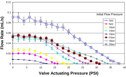
and which operates at up to 30 psi flow pressure. This
method for defining microfluidic devices offers higher
pressure tolerance and more resistance to corrosive
solvents, as delamination problems can be avoided. It
also enables a great flexibility in choice the of
replicated polymers and three-dimensional
interconnection topologies in forming complex
microfluidic circuits for microbiochemical analysis.
2. Chemically robust three-dimensional monolithic SIFEL
fluoropolymer microfluidics
The three-dimensional nature of the “lost wax” valves
valves for microfluidics. This is important because
PDMS, the standard polymer used for microfluidics,
cannot be used with most organic solvents – putting the
most interesting applications of microfluidics out of
reach of the current technologies. Sifel microfluidics
will allow a wider range of solvents and reactions to
be performed in microfluidics.
3. Microfluidic valves for customized radioactive
positron emission dyes
The “lost wax” process was used to create specialized
chips and newly designed, chemically robust,
high-pressure microfluidic valves for making radioactive
positron emission dyes. This is important because
these species typically have very short half-lives,
meaning that all PET scan machines must be within a
certain time-distance from a central manufacturing
site. In turn this causes the central plant to only
produce the standard dye, even though researchers have
been able to create target-specific dyes for use in
more informative diagnostics. The development of local
capacity to create dye as needed in a microfluidic
device would also easily be able to make the more
4. Reducing Microfluidic Control Inputs Through the Use
of Pressure Multiplexing
An important problem in microfluidics is reducing the
number of input pins needed to control as many valves
as possible. Each input pin takes up space on the chip
and requires a leak-free connection to outside plumbing
and large control valves. Using our new
three-dimensional valves created by rapid prototyping we were
able to conceive of and prove a new system of pressure
multiplexing that can greatly reduce the number of
needed inputs beyond the previously reported minimum of
controlling n valves with 2 log2n inputs. We were able to control n valves with 2 log24n inputs.
Furthermore, our pressure multiplexing technique is
general and can be applied to standard 2D
microfluidics. Minimizing the number of control inputs
is extremely important in creating simplified and more
robust microfluidic chips for practical purposes.
5. Bicuspid-inspired microfluidic check valve
Complicated “check valves” can be made using the “lost
wax” process which mimic the operation of the heart’s
valves. These one-way valves promise to be a robust
check valve for an electrically operated microfluidic
three-dimensional valves are analyzed and a one input
pump is demonstrated, as opposed to the three normally
required for traditional peristaltic microfluidic
pumps.
6. Microfluidic Three-Dimensional separation column
The three dimensional rapid prototyping machine is used
to create microfluidic separation columns. Silica is
poured into a tall vertical column and sodium silicate
is used to form the frit. These columns can be easily
made in parallel and complex combinatorial chemical
reactions can be carried out with the products being
purified simultaneously.
III. Devices created to analyze blood
This section deals with microfluidic devices that process
whole blood from a fingerprick and analyzes for various
different proteins
1. Microfluidic Device to extract Blood Plasma from a
finger stick
With the increased use of microfluidic technology in
the fields of physics, chemistry, engineering,
increasingly more important to discover more viable and
more efficient means through which to incorporate
existing technology into a microfluidic context. One
such example is the analysis of blood through
microfluidics. For the practical application of
microfluidic analysis, it is necessary to create a
system of blood filtration and anti-coagulation, a
procedural practice necessary for microscale
whole-blood analysis.
In the context of microfluidic blood analysis, the
system of blood filtration and anti-coagulation is
necessary to handle blood samples in a miniaturized
format. That is to say, there must be a way to separate
blood cells and plasma from whole blood, on a
microfluidic scale, for proper microfluidic blood
analysis.
2. Inexpensive, portable immunoassay device
We have developed an inexpensive and rapid read-out
system for multi-antigen microfluidic fluorescence
immunoassay systems. The fluidic analysis chips can be
fabricated in polydimethylsiloxane PDMS, and have been
shown to perform high-throughput analysis on multiple
analytes and manage the measurement of over 100
fluorescent readings with sensitive detection down to
intensity of fluorescence is used to read the
concentration of the antigen, and is typically measured
with a fluorescence microscope or a laser scanner. This
serial measurement process is both time-consuming and
expensive, and limits the speed with which an
immuno-assay can be completed. Here we show that it is
possible to perform fluorescence detection with digital
imaging to obtain multiple immunoassay readings in
parallel.
a. Use in small cell lung carcinoma
Here we describe the application of a
microfluidic fluorescent noncompetitive
immunoassay system for the detection of the CRMP5
protein, a marker for SCLC (Small Cell Lung
Carcinoma), and the miniaturization of the
detector. Using monoclonal rat antibodies, an
immunoassay stack specific to the CRMP5 marker was
built and tested for specificity and sensitivity.
A microfluidic filter able to separate serum from
blood allowed for tests to examine marked blood. A
detector consisting of an excitation and emission
filter set, lens, LED, and CCD digital camera
replaced bulkier optical microscope detectors and
allowed for images to be taken simultaneously off
all chambers in the microfluidic device. By
the miniaturized detector and using the
immunoassay chip in tandem with microfluidic blood
filters we approach cost-efficient handheld
devices capable of detecting SCLC with high
specificity and sensitivity.
b. Use in multiple sclerosis
Recent advances in microfluidics have allowed
for the fabrication of miniaturized, highly
efficient immunoassay chips that minimize the
quantities of reagent and patient serum needed for
disease detection. This technology is especially
applicable for detection and diagnosis of multiple
sclerosis (MS), a debilitating auto-immune
disease. We were able to demonstrate disease
detection by identifying matrix metalloproteinase
9 (MMP-9), a biomarker for MS, in simulated
patient serum. This is a proof-of-concept for the
viability of a handheld multiple sclerosis symptom
detector. Such a detector could prove invaluable
in the treatment of this disease. Multiple
sclerosis is a disease that progresses through a
series of excacerbations. If these excacerbations
can be predicted through constant monitoring of
blood species, treatments can be developed for use
at the onset of MS attacks in order to minimize or
3. Device to screen metastasizing cancer cells
With nanofabricated microfluidic systems, we studied
the migration behaviors of two cell lines in vitro.
Cells were allowed to migrate through areas of 15 µm in
height, containing a microfluidic channel of 15 µm
(height) by 15 µm (width) and 45 µm to 1cm in length.
We observed that cells left their monolayer origin as
individual cells to enter the entrance of the channel.
After migration through the channel, the daughter cells
resulting from the first division migrated away from
each other to form two colonies. When each of the two
colonies expanded into 32-cell colonies, the colonies
disassociated into multiple small colonies. Our results
indicate that cells can break off from the monolayer to
actively search their environment, and the dissociation
of cells from each other is highly regulated. Future
gene expression profiling study on cells prior and post
disassociation should reveal genes that regulate the
disassociation of cells from the monolayer. These genes
are potential candidate genes which regulate cancer
cells to leave the original tumor and become the
metastasis. We demonstrated here that a microfluidic
system can be a powerful means to study genes that
regulate cell disassociation, which is a first step of
to an inexpensive high throughput device to screen
drugs for inhibiting metastasis in the pharmaceutical
industry.
IV. Devices created to perform polymerase chain reactions
This section deals with temperature control in microfluidics
and its use in PCR
1. Evaporative cooling in microfluidic channels
Evaporative cooling is an effective and energy
efficient way to rapidly remove heat from a system.
Specifically, evaporative cooling in microfluidic
channels can provide a cost-effective solution for the
cooling of electronic devices and chemical reactors.
Here we present microfluidic devices fabricated by
using soft-lithography techniques to form simple
fluidic junctions between channels carrying refrigerant
and channels carrying N2 gas. The effects of channel
geometry and delivery pressure on the performance of
refrigeration through vaporization of acetone,
isopropyl alcohol, and ethyl ether were characterized.
By varying gas inlet pressures, refrigerants, and
angles of the microfluidic junctions, optimal cooling
conditions were found. Refrigeration rates in excess of
40 °C/s were measured, and long lasting subzero cooling
2. Thermal management in microfluidics using
micro-Peltier junctions
We report refrigeration and heating of nanoliter fluid
volumes with micro-Peltier junctions. The temperature
of small liquid reservoirs can be rapidly changed and
controlled within a range between −3 °C to over 120 °C
with good long-term stability. These thermal management
systems enable the fabrication of complex chip-based
chemical and biochemical reaction systems in which the
temperature of many processes can be controlled
independently.
3. Microfluidic Polymerase Chain Reaction
We implement Microfluidic technology to miniaturize a
thermal cycling system for amplifying DNA fragments. By
combining microfluidic thermal heat exchanger to cool a
Peltier junction, we have demonstrated very fast
heating and cooling of small volumes of solution. We
use a miniature K-type thermocouple to provide a means
for in-situ sensing of the temperature inside the
micro-refrigeration system. By combining the
thermocouple, two power supplies controlled with a
relay system, and computer automation, we reproduce the
demonstrated amplification of a DNA sample of about
1000 bp.
4. Accessible Polymerase Chain Reaction
Since the mid-1990s, real-time polymerase chain
reactions (PCR) have been used with selective primers
to amplify and identify DNA and RNA molecules within
large and expensive thermal cyclers. Recently, it has
become possible to build compact heating and cooling
systems for the amplification of DNA with greater
accuracy at a 100 times lower cost. Such inexpensive
PCR identification could serve remote regions of the
world, leading to an early warning system for pandemic
outbreaks. Here we compare a portable PCR system with a
conventional desk-top unit. We show that H5N1 (avian
influenza) and HIV (AIDS), as well as many other common
virus strains can be identified within a clinical
setting at low viral loads. Our portable instrument
results in superior amplification as more precise
temperature control is possible. This improvement in
performance also enables the use of less expensive
intercalating dyes as fluorescent probes, further
I
Devices exploring basic areas of physical and biological
1. Surface plasmon enhanced InGaN light emitting
diode
ABSTRACT
We report a dramatic increase in the photoluminescence (PL)
emitted from InGaN/GaN quantum wells (QW), obtained by
covering these sample surface with thin metallic films.
Remarkable enhancements of PL peak intensities were obtained
from In0.3Ga0.7N QWs with 50 nm thick silver and aluminum
coating with 10 nm GaN spacer. These PL enhancements can be
attributed to strong interaction between QWs and surface
plasmons (SPs). No such enhancements were obtained from
samples coated with gold, as its well-known plasmon
resonance occurs only at longer wavelengths. We also showed
that QW-SP coupling increase the internal quantum
efficiencies (•int) by measuring the temperature dependence of PL intensities. QW-SP coupling is a very promising method
for developing the super bright light emitting diodes
(LEDs). Moreover, we found that the metal nano-structure is
very important facto to decide the light extraction. A
possible mechanism of QW-SP coupling and emission
enhancement has been developed, and high-speed and efficient
light emission is predicted for optically as well as
electrically pumped light emitters.
1. INTRODUCTION
Since 1993, InGaN quantum wells (QW)-based light emitting
diodes (LEDs) have been continuously improved and
visible spectral regions.1-3 Moreover, white light LEDs, in
which a blue LED is combined with a yellow phosphor, have
been commercialized and offer a replacement for conventional
incandescent and fluorescent light bulbs.4 However, the
promise of inexpensive solid state lighting has so far been
delayed by the relatively poor extraction efficiency of
light from semiconductor light sources. We believe that the
development of efficient and bright white LEDs will rapidly
result in commercialization of efficient solid state
illumination sources. The most important requirement for a
competitive LED for solid state ligthing is the development
of new methods to increase its quantum efficiency of light
emission.
The external quantum efficiency (•ext) of light emission from an LED is given by the light extraction efficiency (Cext) and internal quantum efficiency (•int). •int in turn is determined by the ratio of the radiative (krad) and nonradiative (knon) recombination rates of carriers.
non rad rad ext ext ext k k k C C + × = × = ηint
η (1)
Often, knon is faster than krad at room temperature, resulting in modest •int. There are three methods to increase •ext; (1) increase Cext, (2) decrease knon, or (3) increase krad. Previous work has focused on improving Cext from InGaN LEDs by using the patterned sapphire substrates and mesh electrodes.5
However, further improvements of extraction of light through
limitations. Although much effort has recently been placed
into reducing knon by growing higher quality crystals,6-7
dramatic enhancements of •ext have so far been elusive. 8-9 On the other hand, there have been very few studies focusing on
increasing krad,10-11 though that could prove to be most
effective for development of high •ext light emitters. In this article, we propose the enhancement of krad by coupling
between surface plasmon (SP) and the InGaN QWs. If the
plasmon frequency is carefully selected to match the QW
emission frequency, the increase of the density states
resulting from the SP dispersion diagram can result in large
enhancements of the spontaneous emission rate. Therefore,
energy coupling between QW and SP as described in this
article is one of the most promising solutions to increase
krad. SPs, excited by the interaction between light and metal surfaces,12-13 are known to enhance absorption of light in
molecules14, increase Raman scattering intensities15-16 and
light transparencies17-18, and also generate photonic band
gap19-20. Since 1990, SPs have also received much attention
when used in LEDs21-30. Gianordoli et al optimized the
emission characterization of GaAs-based LED by SP.25 Vuckovic
et al. reported the SP enhanced LED analyzing by both
theoretically and experimentally.26 Thus, great attention has
been focused on SP enhanced emission. Hobson et al. reported
the SP enhanced organic LEDs.27 For InGaN QWs, Gontijo and
co-workers reported the coupling of the spontaneous emission
increased absorption of light at the SP frequency. Neogi et
al. confirmed that the recombination rate in an InGaN/GaN QW
could be significantly enhanced by the time-resolved PL
measurement.29 However, in this early work, light could not
be extracted efficiently from the silver/GaN surface.
Therefore, the actual PL enhancement of InGaN/GaN by
coupling into SP had not so far been observed directly.
Quite recently, we have reported for the first time large
photoluminescence (PL) increases from InGaN/GaN QW material
coated with metal layers.30 In order to design even more
efficient structures and to fabricate electrical pumped LED
devices by using SP coupling, we have to understand and
optimize both mechanism and dynamics of energy transfer and
light extraction. Here we fabricate and test nano-structured
metal layers to explore the dependence of the plasmon
enhancement on metal composition, thickness and grain shapes
and sizes. The purpose of this work is to predictably use
our control over metal geometries and composition to improve
light emission and localization.
2. EXPERIMENT
Fig 1 shows the setup of the PL measurement and the sample
structure. In0.3Ga0.7N/GaN QW wafers were grown on a (0001) oriented sapphire substrate by a metal-organic chemical
vapor deposition (MOCVD). The QW heterostructure consists of
a GaN (4 •m) buffer layer, an InGaN QW (3 nm) and a GaN cap
layer (10, 40 or 150 nm), and the PL peak wavelength of the
evaporated on top of the surface of these wafers. After
polishing the bottom surface of the QW samples, we
photoexcite and detect emission from the backside of the
samples through the transparent substrate. Such back side
access to the QWs permit us the rapidly compare the PL from
QWs with and without the influence of SPs, and to measure
the dependence of the emission intensity on the distance
between the QW and the metal films by changing the GaN
spacer thickness. Topography measurements were performed by
a twin-SNOM system manufactured by OMICRON. Fluorescence
microscopy was used with X40 objective, a mercury lamp, and
a color CCD camera. Metal grating structures were fabricated
by electron beam lithography on a 50 nm thick
polymethylmethacrylate (PMMA) mask coated on the metal
surface. The pattern was transferred into the top metal
layer by using Ar ion milling.
To perform the photoluminescence (PL) measurements, a
cw-InGaN diode laser (406 nm) was used to excite the QWs from
the bottom surface of wafer. Luminescence was collected and
focused into an optical fiber and subsequently detected with
a multichannel spectrometer (Ocean optics). Neutral density
Fig. 1 Experimental setup of the photoluminescence
measurement and the sample structure.
excitation power (from 0.18 to 4.5 mW) to determine the
power dependence of the luminescence intensities, and their
temperature dependence was studied by using a by cryostat
with the ability of cooling from room temperature to 6K. To
perform time-resolved PL measurements, frequency doubled
beams of a mode-locked Al2O3:Ti laser pumped by an Ar+ laser were used to excite the QW from the backside of the wafer. A
1.5 ps pulse width, 400 nm pump wavelength, and 80 MHz
repetition rate were chosen to excite luminescence in the
QW. A streak camera system (Hamamatsu) was used as the
detector.
3. RESULTS AND DISCUSSIONS
3.1 Enhanced photoluminescence spectra
Fig. 2a shows typical emission spectra from InGaN/GaN QW
samples covered with silver layers. As the PL peak of the
uncoated wafer at 470 nm was normalized to 1, it is clear
that a dramatic enhancement in the PL intensity from the
thicknesses is limited to 10 nm. On the other hand, the PL
intensities are no longer strongly influenced from the
silver in samples with 150 nm thick cap layers. The
enhancement ratios of 10 nm capped QW samples covered with
silver are 14-fold at the peak wavelength and 17-fold when
comparing the luminescence intensity integrated over the
emission spectrum with un-coated InGaN samples. We also
compared the PL spectra of our QW samples after coating them
with silver, aluminum, and gold layers (Fig. 2b). For InGaN
QWs with a 10nm cap, such measurements indicate that a
8-fold peak intensity and 6-8-fold integrated intensity
enhancement is obtained after coating with aluminum, and no
enhancement in PL is found to occur in gold-coated samples.
In such a measurement, a small (2x) increase in the
luminescence efficiency could be expected after
metallization as the deposited metal reflects light back
into the QW, and this may double the effective path-length
of the incident pump light. Although the reflectivity of
gold at 470 nm is smaller than that of silver or aluminum,
this difference alone cannot explain the large difference in
the enhancement ratio of each metal.
The dramatic PL enhancement of samples after coating with Ag
and Al can be attributed to the strong interaction between
the QW and SPs. We propose a possible mechanism of QW-SP
coupling and light extraction shown in Fig. 3a.
Electron-hole pairs created in the QW can couple to the electron
bandgap energy (••BG) of InGaN active layer is close to the electron vibration energy (••SP) of SP. Then, electron-hole recombination may produce a SP instead of a photon, and this
new path of the recombination increases the spontaneous
recombination rate. If the metal/semiconductor surface were
perfectly flat, it would be difficult to extract light
emission from the SP, since it is a non-propagating
evanescent wave. However, in evaporated metal coatings,
light emission can be observed as the SP is scattered
through roughness and imperfections in the metal layers. The
coupling rate (kSP) between the QW and SP is expected to be much faster than krad as a result of the large electromagnetic fields introduced by the large density of states (Fig. 3b).
Actually, we observed such the enhanced spontaneous emission
rates
Fig. 2 a, PL spectra of InGaN/GaN QWs coated with silver
spectra of InGaN/GaN coated with Ag, Al and Au with 10 nm
GaN spacers.
by the time-resolved PL measurement. All profiles could be
fitted to single exponential functions and PL lifetimes (•PL) were obtained. We found that the time-resolved PL decay
profiles of the Ag-coated sample strongly depend on the
wavelength and become faster at shorter wavelengths, whereas
those of the uncoated sample show little spectral
dependence.31 We attribute the increases in both emission
intensities and decay rates from Ag-coated samples to the
coupling of energy between the QW and the SP.
3.2 Surface plasmon dispersion diagram
The dispersion diagrams of the SP modes at the metal/GaN
interfaces are shown in Fig. 4a. The SP wave-vector
(momentum) k(•) was obtained by the following equation.12-13
) ( ' ) ( ' ) ( ' ) ( ' ) ( ω ε ω ω ε ω ε ω ϖ GaN metal GaN metal e c k + = (2)
where, •‘metal(•) and •‘GaN(•) are the real part of the
dielectric functions for metal and GaN, respectively. The
plasmon energy (••P) of silver is well known as 3.76 eV.32 The SP energy (••SP) must be modified for a silver/GaN surface, and can be estimated to be approximately ~2.8 eV (~440 nm)
(Fig. 4a) when using the dielectric constant of silver33 and
GaN34. k(•) approaches infinity around ~2.8 eV by •‘metal(•) +
was very close to ••SP, and large SP enhancements in luminescence intensity were observed especially at the
higher energy side of the PL spectrum. This observation
supports the existence of the QW-SP coupling phenomenon.
Thus, silver is suitable for SP coupling to blue emission,
and we attribute the large increases in luminescence
intensity from Ag-coated samples to such resonant SP
excitation. In contrast, the estimated ••SP of gold on GaN is below ~2.2 eV (~560 nm), and no measurable enhancement is
observed in Au-coated InGaN emitters as the SP and QW
energies are not matched. In the case of aluminum, the ••SP is higher than ~5 eV (~250 nm), and the real part of the
dielectric constant is negative over a wide wavelength
region for visible light.35 Thus, a substantial and useful PL
enhancement is observed in Al-coated samples, although the
energy match is not ideal at 470 nm and a better overlap is
expected at shorter wavelengths. Fig. 4b shows the
enhancement ratios of PL intensities with metal layers
separated from the QWs by 10 nm spacers as a function of
wavelength. We find that the enhancement ratio increases at
shorter wavelengths for Ag samples, while it is independent
of wavelength for Al coated samples. The clear correlation
between Figs.4a and 4b suggests that the obtained emission
Fig. 3 a, Schematic diagram of the electron-hole
recombination and QW-surface plasmon (SP) coupling
mechanism. b, Energy diagram of excitation, emission and
QW-SP coupling.
3.3 Spacer trickiness and excitation power dependences
PL intensities of Al and Ag coated samples were also found
to strongly depend on the distance between QWs and the metal
layers, in contrast to Au coated samples. Fig. 5a shows this
dependence of the PL enhancement ratios taken for three
different GaN spacer thicknesses (of 10nm, 40nm, and 150nm)
with each metal coating. These show an exponential increase
in intensity as the spacer thickness is decreased for Ag and
Al, but no significant improvement in the PL intensity for
samples coated with gold. This figure suggests that coupling
between SP should be main component to contribute to the PL
enhancement, because the SP is an evanescent wave, which
surface. Only electron-hole pairs located within the
near-field from the surface can couple to the SP mode. The
penetration depth Z(•) of the SP fringing field into GaN
from metal can be calculated from11-12
2 ) ( ' ) ( ' ) ( ' ) ( ω ε ω ε ω ε ω ω metal metal GaN c
Z = − (3)
Z(•) is predicted to be Z= 47, 77, and 33 nm for Ag, Al, and
Au, respectively at 470 nm. The inset of Fig. 5a shows good
agreement between these calculated penetration depths
(dashed lines) and measured values for Ag and Al coated
samples. This again indicates that the emission enhancement
results from QW-SP coupling.
We also find that the luminescence enhancement ratio
increases with increasing excitation power (Fig. 5b). In
InGaN QWs, electron-hole pairs are often localized by
spatial modulations in bandgap energy produced by
fluctuations of indium composition, QW width, or
piezoelectric field. Such localization centers serve as
radiative recombination centers for electron-hole pairs and
explain the strong emission and insensitivity to growth
defects in InGaN/GaN QW material. The emission efficiency
may be reduced at high excitation intensities by saturation
of these localization centers. When metal layers are coated
within the near field of the QW, both localized and
un-localized electron-hole pairs can immediately couple to the
SP mode. In that situation, the saturation of the localized
efficiencies even under intense excitation. We consider this
very advantageous in light emitting diodes, since generally
the emission efficiencies of such emitters are reduced under
the high current pumping. Thus, by using the SP coupling,
higher current operation and brightness should be
achievable.
3.4 Internal quantum efficiencies and Purcell enhancement
factor
We expect that the SP coupling will increase the efficiency
(•int) by enhancing the spontaneous recombination rate. In order to estimate the •int and to separate the SP enhancement from other effects (mirror effect, photon recycling, etc.),
we have also measured the temperature dependence of the PL
intensity. Fig. 6a shows the linear and Arrhenius plots of
the integrated photoluminescence intensities of InGaN-SQWs
coated with Ag and Al and compares these to un-coated
Fig. 4 a, Dispersion diagrams of surface plasmons generated
InGaN/GaN. b, PL enhancement ratios at several
wavelengthsfor same samples with Fig. 2b.
samples with 10 nm GaN spacer layer thicknesses. The •int values of un-coated InGaN was estimated as 6 % at room
temperature by assuming •int ~100% at ~6 K.36 We found that the •int values were increased by 6.8 times (41%) by Ag coating and by 3 times (18%) by Al coating. We expect this actual
enhancement of the •int values to be a result of the enhancement of the spontaneous recombination rate of
electron-hole pairs by SP coupling. 6.8-fold increasing of
•int means that 6.8-fold improvement of the efficiency of
electrically pumped LED devices should be achievable because
•int is a fundamental property and not depend on the pumping method. Such improved efficiencies of the white LEDs, in
which a blue LED is combined with a yellow phosphor, are
expected to be larger than those of current fluorescent
lamps or light bulbs. The luminous efficacy of commercial
white LEDs is 25 lm/W under a current of 20 mA at room
temperature.37 This value is still lower than that of
fluorescent tubes (75 lm/W). A 3-fold improvement is
necessary to exceed the current fluorescent lamps or light
bulbs. We expect that the SP coupling technique is very
promising for even larger improvements of solid-state light
Wavelength depended enhanced efficiencies •int*(•) can be related the coupling rate kSP(•) between QWs and SPs by the relationship:
Fig. 5. GaN spacer thicknesses (a) and excitation power (b)
dependence of the PL enhancement ratios.
Fig. 6 a, Temperature dependence of integrated PL
intensities. b, Wavelength dependent emission efficiencies
[•int*(•)] was plotted as dashed line. The Purcell
(solid line). The dotted line was the PL spectrum of the same sample. ) ( ) ( ) ( ) ( ) ( ) ( ) ( ' *
int ω ω ω
ω ω ω ω η SP non rad SP ext rad k k k k C k + + + = (4)
where C’ext(•) is the probability of photon extraction from the SPs energy and is decided by the ratio of light
scattering and dumping of electron vibration through
non-radiative loss. Fig, 6b shows the •int*(•) of Ag coated sample estimated from PL enhancement ratio (Fig. 6b) by
normalizing the integrated •int* should be 41%. We find that •int*(•) increases at shorter wavelengths where the plasmon resonance more closely matches the QW emission, and reaches
almost 100% at 440 nm.
The Purcell enhancement factor Fp38 quantifies the increase in the spontaneous emission rate of a mode for a particular
mode, and can be described by •int(•) and •int*(•) when C’ext•1:
) ( 1 ) ( 1 ) ( ) ( ) ( ) ( ) ( ) ( * int int ω η ω η ω ω ω ω ω ω − − ≈ + + + = non rad SP non rad p k k k k k F (5)
Fig.6b also shows Fp(•) estimated at each wavelength by assuming a constant •int(•) = 6 %. Fp(•) is significantly higher at wavelengths below 470 nm, well in agreement with
previous work28-29. The PL spectrum shape (plotted as dotted
line) also indicates that Fp(•) values are higher at the shorter wavelength region. That should be a possible reason
for the asymmetry in the luminescence peak of Fig. 2. Fig.
440 nm should be best matched for SP enhancement from a
silver layer. In that case, the enhanced •int*(•) value is expected to approach 100% throughout the PL spectrum. The SP
frequency could be geometrically tuned to match our • ~ 470
nm QW by fabricating nanostructures, for example, using a
grating structure, or using alloys.
3.5 Surface roughness and grating structures
The SP energy can be extracted as light by providing
roughness or nano-structuring the metal layer. Such
roughness allows SPs of high momentum to scatter, lose
momentum and couple to radiated light.39 C’ext(•) in Eq.(4) should depend on the roughness and nano-structure of the
metal surface. We succeeded in controlling the grain
structure within nano-sizes. Such roughness in the metal
layer was observed from topographic images obtained by
shear-force microscopy of the original GaN surface (Fig. 7a)
and the coated Ag surface (Fig. 7b). The depth profiles
Fig. 7 Topographic image of the uncoated GaN surface (a) and
the 50 nm thick Ag film evaporated on GaN (b). The
depthprofilealong the dashed line in the topographic images
are also plotted.
dashed lines of the Ag surface of approximately 30-40 nm
while the GaN surface roughness was below 10 nm. Higher
magnification SEM images of Ag and GaN surface are shown in
Figs. 8a and 8b. The length scale of the roughness of Ag
surface was determined to be a few hundred nanometers. Fig.
8c shows a fabricated metal grating, a geometry that has
previously been used to couple SP and photons 21, 23-26.
Micro-luminescence images of uncoated, coated, and patterned
grating structures of Ag on InGaN QWs with 10 nm spacers are
133 nm wide Ag stripes forming a 400 nm period grating,
whereas such an emission increase was not observed from 200
nm wide Ag stripes within a 600 nm period grating. This
measurement suggests that the size of the metal structure
determines the SP-photon coupling and light extraction. We
also found that the PL peak position of grating structured
regions was dramatically blue-shifted (Fig. 9). This
suggests that the nano-grating structure modulate not only
light extraction but also localized SP frequency. Such
geometrical tuning of the SP frequency is one of the most
important next subjects and is now on progress by
Fig. 8 SEM images of (a) the uncoated GaN surface, (b) the
50 nm Ag film on GaN, and (c) the grating structure with 33%
duty cycle fabricated within a 50 nm thick Ag layer on GaN.
(d) Micro-luminescence image including the areas of Figs.
Fig. 9 PL spectra of InGaN/GaN QW with nano-grating
structured and unstructured silver layers with 10 nm GaN
4. CONCLUSIONS
We conclude that the SP enhancement of PL intensities of
InGaN is a very promising method for developing solid state
light sources with high emission efficiencies. We have
directly measured significant enhancements of •int and the spontaneous recombination rate, and shown how distance and
choice of patterned metal films can be used to optimize
light emitters. Even when using un-patterned metal layers,
the SP energy can be extracted by the submicron scale
roughness on the metal surface. SP coupling is one of the
most interesting solutions for developing efficient photonic
contact and for providing high electromagnetic fields from
SPs. We believe that this work provides a foundation for the
rapid development of highly efficient and high-speed solid
state light emitters alternative to conventional light
bulbs.
REFERENCES
1. S. Nakamura, T. Mukai and M. Senoh, “Candela-class
high-brightness InGaN/AlGaN double-heterostructure
blue-light-emitting diodes”, Appl. Phys. Lett. 64, 1687-1689,
1994.
2. S. Nakamura, T. Mukai, M. Senoh and N. Iwase,
“High-brightness InGaN/AlGaN double-heterostructure
blue-green-light-emitting diodes”, J. Appl. Phys. 76, 8189-8191, 1994.
3. T. Mukai, M. Yamada, S. Nakamura, “Current and
temperature dependences of electroluminescence of
InGaN-based UV/blue/green light-emitting diodes”, Jpn. J. Appl.
Phys. 37, L1358-L1361, 1998.
4. S. Nakamura and G. Fasol, The blue laser diode: GaN
based light emitting diode and lasers, Springer, Berlin,
1997.
5. M. Yamada, T. Mitani, Y. Narukawa, S. Shioji, I.
Niki, S. Sonobe, K. Deguchi, M. Sano, and T. Mukai,
“InGaN-based near-ultraviolet and blue-light-emitting diodes with
high external quantum efficiency using a patterned sapphire
substrate and a mesh electrode”, Jpn. J. Appl. Phys. 41,
6. S. Nakamura, “The roles of structural imperfections
in InGaN-based blue light-emitting diodes and laser diodes”,
Science, 281, 956-961, 1998.
7. S. Nakamura, M. Senoh, S. Nagahama, N. Iwasa, T.
Yamada, T. Matsushita, H. Kiyoku, Y. Sugimoto, T. Kozaki,
“InGaN/GaN/AlGaN-based laser diodes with modulation-doped
strained-layer superlattices grown on an epitaxially
laterally overgrown GaN substrate”, Appl. Phys. Lett. 72,
211-213, 1998.
8. T. Mukai, K. Takekawa, S. Nakamura, “InGaN-based
blue light-emitting diodes rrown on epitaxially laterally
overgrown GaN substrates”, Jpn. J. Appl. Phys. 37,
L839-L841, 1998.
9. T. Mukai, and S. Nakamura, “ultraviolet InGaN and
GaN single-quantum-well-structure light-emitting diodes
grown on epitaxially laterally overgrown GaN substrates”,
Jpn. J. Appl. Phys., 38, 5735-5739, 1999.
10. P. Walterelt, O. Brandt, A. Trampert, H. T. Grahn,
J. Menniger, M. Ramsteiner, M. Reiche, and K. H. Ploog,
“Nitride semiconductors free of electrostatic fields for
efficient white light-emitting diodes”, Nature, 406,
865-868, 2000.
11. J. J. Wierer, M. R. Krames, J. E. Epler, N. F.
Gardner, M. G. Craford, J. R. Wendt, J. A. Simmons, and M.
M. Sigalas, “InGaN/GaN quantum-well heterostructure
light-emitting diodes employing photonic crystal structures” Appl.
12. H. Raether, Surface plasmon on smooth and rough
surface and on grating, Springer, Berlin, 1988.
13. A. Liebsch, Electronic Excitations at Metal
Surfaces, Physics of Solids and Liquids, Ansgar, Libsch,
1997
14. G. W. Ford and W. H. Weber,
“Electromagnetic-interactions of molecules with metal-surfaces”, Phys. Rep.
113, 195-287, 1984.
15. M. Fleischmann, P. J. Hendra, and A. J. McQuillan,
“Raman spectra of pyridine adsorbed at a silver electrode”,
Chem. Phys. Lett. 26, 163-166, 1974.
16. J. F. García-Vidal, and J. B. Pendry, “Collective
theory for surface enhanced Raman scattering”, Phys. Rev.
Lett. 77, 1163-1166, 1996.
17. T. W. Ebbesen, H. J. Lezec, H. F. Ghasemi, T. Thio,
and P. A. Wolff, “Extraordinary optical transmission through
sub-wavelength hole arrays”, Nature, 391, 667-669, 1998.
18. U. Schroter and D. Heitmann,
“Surface-plasmon-enhanced transmission through metallic gratings”, Phys. Rev.
B, 58, 15419-15421, 1998.
19. S. C. Kitson, W. L. Barnes, and J. R. A. Sambles,
“full photonic band gap for surface modes in the visible”,
20. W. T. Barnes, T. W. Preist, S. C. Kitson, and J, R.
Sambles, “Physical origin of photonic energy gap in the
propagation of surface plasmon on grating”, Phys. Rev.B. 54,
6227-6244, 1996.
21. A. Köck, E. Gornik, M. Hauser, and M. Beinstingl,
“Strongly directional emission from AlGaAs/GaAs
light-emitting diode”, Appl. Phys. Lett. 57, 2327-2329, 1990.
22. N. E. Hecker, R. A. Hopfel, and N. Sawaki, Physica
E, “Enhanced light emission from a single quantum well
located near a metal coated surface”, 2, 98-101, 1998.
23. N. E. Hecker, R. A. Hopfel, N. Sawaki, T. Maier,
and G. Strasser, “Surface plasmon-enhanced photoluminescence
from a single quantum well”, Appl. Phys. Lett. 75,
1577-1579, 1999.
24. W. L. Barnes, “Electromagnetic crystals for surface
plasmon polaritons and the extraction of light from emissive
devices”, J. Light. Tech., 17, 2170-2182, 1999.
25. S. Gianordoli, R. Hainberger, A. Kock, N. Finger,
E. Gornik, C. Hank, and L. Korte, “Optimization of the
emission characteristics of light emitting diodes by surface
plasmons and surface waveguide modes”, Appl. Phys. Lett. 77,
2295-2297, 2000.
26. J. Vuckovic, M. Loncar, and A. Scherer, “Surface
plasmon enhanced light-emitting diode”, IEEE J. Qunt. Elec.
27. P. A. Hobson, S. Wedge, J. A. E. Wasey, I. Sage,
and W. L. Barnes, “Surface plasmon mediated emission from
organic light emitting diodes”, Advanced Materials, 14,
1393-1396, 2002.
28. I. Gontijo, M. Borodisky, E. Yablonvitch, S.
Keller, U. K. Mishra, and S. P. DenBaars, “Enhancement of
spontaneous recombination rate in a quantum well by resonant
surface plasmon coupling” Phys. Rev. B, 60, 11564 -11567,
1999.
29. A. Neogi, C.-W. Lee, H. O. Everitt, T. Kuroda, A.
Tackeuchi, and E. Yablonvitch, “Enhancement of spontaneous
recombination rate in a quantum well by resonant surface
plasmon coupling”, 66, 153305, 2002.
30. K. Okamoto, I. Niki, A. Shvartser, Y. Narukawa, T.
Mukai, A. Scherer, “Surface-plasmon-enhanced light emitters
based on InGaN quantum wells”, Nature Mater., 3, 601-605,
2004.
31. K. Okamoto, I. Niki, Y. Narukawa, T. Mukai, Y.
Kawakami, and A. Scherer, “Surface plasmon enhanced
high-speed spontaneous emission”, submitted for publication
32. A. Liebsch, “ Surface plasmon dispersion of Ag”,
Phys. Lev. Lett, 71, 145-148, 1993.
33. E. D. Palik, Handbook of Optical Constants of
solids, Academic, San Diego, 1985.
34. T. Kawashima, H. Yoshikawa, S. Adach, S. Fuke, and
K. Ohtsuk, “Optical properties of hexagonal GaN”, J. Appl.
35. A. Bagchi, C. B. Duke, P. J. Feibelman, and J. O.
Porteus, “ Measurement of Surface-Plasmon Dispersion in
Aluminum by Inelastic Low-Energy Electron Diffraction”,
Phys. Rev. Lett., 27, 998–1001, 1971.
36. Y. Kawakami, K. Omae, A. Kaneta, K. Okamoto, T.
Izumi, S. Saijo, K. Inoue, Y. Narukawa, S. Nakamura, and S.
Fujita, ”Radiative and nonradiative recombination processes
in GaN-based semiconductors”, Phys. Stat. Sol. (a), 183,
41-50, 2001.
37. Y. Narukawa, I. Niki, K. Izuno, M. Yamada, Y.
Murazaki and T. Mukai, “hosphor-conversion white light
emitting diode using InGaN near-ultraviolet chip”, Jpn. J.
Appl. Phys. 37, L371-L373, 2003.
38. E. M. Purcell, “Spontaneous emission probabilities
at radio frequencies”, Phys. Rev. 69, 681, 1946.
39. W. Barnes, “Light-emitting devices: Turning the
tables on surface plasmons”, Nature Mater., 3, 588-589,
2. Analysis of using AlGaN emitters coupled with thin film
heaters to cure onychomycosis infections
Onychomycosis affects more than 35 million Americans and is
sometimes life threatening in immunocompromised patients and
can lead to amputations in people with diabetes. Current FDA
approved treatments work very poorly with a 5.5-8.5% chance
of cure for Ciclopirox and a 38% chance for terbinafine
hydrochloride. Additionally terbinafine hydrochloride is
toxic to the liver and has a 15% chance of reinfection. The
recent advances in creating low cost, commercially available
AlGaN LED’s which emit in the UV range, coupled with thin
film heaters has led us to explore the use of these devices
for the treatment of onychomycosis. These systems are
theorized to work through a number of pathways. First the
247-275nm center wavelengths of the LED’s is known to be at
a DNA and RNA absorption peak and light in this energy
Figure 1 Absorption peak of 1. DNA and 2. RNA
The UV absorption of the keratin sheet of the nail can
be measured and a proper UV dose can be used in order to not
overdose the patient. It seems reasonable to assume that a
dose lower than the average daily dose of an exposed digit
would be safe, and our research suggest that this would be
more than enough to kill the fungus. Additionally these
fungi typically grow not only due to dark confines, but also
because the temperature of the nail bed is typically 1-2
degrees lower than body temperature, ideal growing
conditions for these fungi. In addition to the UV light
treatment, a thin film heater is used to create a “localized
fever” in order to create conditions that inhibit fungal
growth. The resistive heater both raises the temperature
and drives off moisture in order to kill the fungi (fig. 1).
themselves or in combination with existing treatments in
order to increase the effectiveness of those treatments.
For the general population it may simply be a matter of
shifting the balance in the person-pathogen interaction in
the favor of the person such that their normal immune system
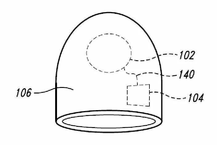
[image:54.612.111.468.219.454.2]can overcome the fungus.
Figure 2 The device as envisioned over the nail, 102 is the combination UV LED and thin film heater, 104 is the power supply, 106 and 140 are the mechanical and electrical connections
We have made some start on the fungus growth, with four
strains (two Trichophyton rubrum and two T. mentagrophytes -
the two most common nail fungi) and about two weeks ago set
up a suit of conditions for one of the T. rubrum. At first
we had some difficulties, likely due to the Tween 20 (fatty
or inhibited the fungus. It is known that some of the long
chain fatty acids inhibit the fungus.
Next one of the T. mentagrophytes species was grown,
with excellent growth at 30°C and 37°C but nothing at
39-40°C, and a UV does of 0.3 min seems to have kill the
fungus. However, this was done on the spores rather than a
growing mat of the fungus, this is less informative as
spores can become dormant, be less (usually more) resistant
to stresses, etc. Interestingly the fungus grows very poorly
on minimal medium, which is strange as many mutants of other
fungi unable to grow on this type of media are unable to
cause disease.
The next step is to test all four strains at once under
the same types of conditions, as well as use the fungus when
it is growing actively rather than in the spore stage.
The devices provided to our collaborators at Duke
University where Petri dishes with embedded LEDs and thin
film heaters and control electronics. The sterility was
guaranteed by wiping around the lid with ethanol, and the
LED was allowed to self-sterilize. The Petri dishes where
poured with 30 ml of growth medium, which gives the agar a
thickness of 5 - 5.5 mm. Depending on the age of the fungus
there can be some distortion in the media, so the light was
made to hit somewhere between 5 and 7 mm. (closer to 5.5 was
ideal). The distance between bottom of the plate to the top
Figure 3 Cryptococcus neoformans exposed to UV light
Cryptococcus fungi was very sensitive to the UV light
(fig. 1). A lawn of Cryptcoccus yeast cells was spread on
plates and treated at 9.3mA for 36 and 70 min, then grown on
the plates overnight. A good clearing of the fungus in the
middle is clearly visible. It is clear that much less
exposure is needed to kill the fungus - probably for
Cryptococcus a few minutes at lower power would work. We
suspect that with this sort of action the nail fungus will
not need days of treatment to be killed.
A trial run on Trichophyton was similarly carried out.
Figure 3 shows a representative sample dosed at 9.85mA,
which while it looks like there is almost even growth, the
clumped look of the UV treated plates are indicative that
only a subset of the fungus survived the treatment, and
later grew back fine - at an earlier time point the
difference is more dramatic. This suggest several further
experiments:
(a) smaller inoculation area - The light is very focused, so
anything on the edge is not exposed
(b) increase the dose up to 2 and 4 h, and
(c) try re-hitting the fungus the next day with a second
treatment.
The treatment of onychomyosis is an important area, and
novel devices such as the AlGaN LEDs and thin film heaters
could present an effective, low side effect treatment
options for millions. As research in this area continues
will be have better dose characteristic data, coupled with
temperature data. The next steps will be to obtain infected
nails from volunteers in order to measure the UV absorption
of keratin in order to ascertain safe doses of ultraviolet
radiation. Next clinical trials, with and without
antifungal compounds can be started.
References:
UV INACTIVATION OF PATHOGENIC AND INDICATOR MICROORGANISMS
APPLIED AND ENVIRONMENTAL MICROBIOLOGY 49 (6): 1361-1365
1985
[2] Brasch J, Menz A. UV susceptibility and negative
phototropism of dermatophytes, Mycoses 38, 197-203 (1995)
[3] Robbins WJ, Growth Requirements of Dermatophytes, Annals
New York Academy of Sciences, 1357
[4] http://www.steribeam.com/puv-rev.htm
[5] Gupta A, Fleckman P, Baran R, Ciclopirox nail lacquer
topical solution 8% in the treatment of toenail
onychomycosis, American Academy of Dermatology, (2000)
[6] Young C, Range of variation among isolates of
3. Tunable organic transistors that use microfluidic source
and drain electrodes
This letter describes a type of transistor that uses
conducting fluidic source and drain electrodes of
mercury which flow on top of a thin film of the organic
semiconductor pentacene. Pumping the mercury through
suitably designed microchannels changes the width of the
transistor channel and, therefore, the electrical
characteristics of the device. Measurements on transistors
with a range of channel lengths reveal low contact
resistances between mercury and pentacene. Data collected
before, during, and after pumping the mercury through the
microchannels demonstrate reversible and systematic tuning
of the devices. This unusual type of organic transistor has
the potential to be useful in plastic microfluidic devices
that require active elements for pumps, sensors, or other
components. It also represents a noninvasive way to build
transistor test structures that incorporate certain classes
of chemically and mechanically fragile organic
semiconductors.
The integration of active electronics directly with
molded microfluidic channel arrays represents a promising
way to increase the functionality, lower the cost, and
reduce the size of microfluidic reactors, separation, and
characteristics—intrinsic compatibility with plastics, ease
of fabrication and processing, ability to be patterned with
the types of soft lithographic methods that are useful for
building microfluidic devices,[1–3] etc.—that make them
attractive for this purpose. Here we explore one route for
directly combining the active elements of plastic circuits
(i.e., the transistors themselves) with moving fluids that
can be coupled in various ways to the microfluidic elements
of the system. We demonstrate, in particular, that
microchannels filled with mercury can serve as dynamically
tunable source and drain electrodes in transistors that
incorporate the p-type organic semiconductor pentacene. This
letter begins with a description of the layout of these
devices and the sequence of steps for their fabrication.
Measurements on transistors with channel lengths between 25
and 200 mm demonstrate the good performance of these devices
and the low contact and parasitic resistances associated
with them. Pumping the mercury back and forth in the
channels reversibly adjusts the electrical characteristics
of the transistors in a systematic and easily understandable
way. Devices with this design could find applications as
sensors or elements of drive circuits for pumps in
microfluidic systems. In addition, the noninvasive and low
resistance microchannel mercury contacts may be useful for
basic studies of charge transport in chemically and
way that is analogous to the recent application of mercury
droplets for probing organic molecular-scale diodes [4].
Figure 1(a) shows a schematic view of a typical device.
Figure 1 Part (a) shows a schematic angled view of a PDMS element with relief on its surface (top) and a substrate that supports the semiconductor, gate dielectric, Ti/Au/Ti contact lines, and gate electrode. Part (b) shows a
schematic illustration of the assembled device as viewed from the top through the transparent PDMS. Part (c) presents optical micrographs of the transistor region with mercury (white) pumped into the channel on the left hand side to various degrees. The extent that the mercury fills the channels defines the effective transistor channel width.
It consists of a bottom substrate that supports a thin film
of an organic semiconductor (pentacene; 25 nm, deposited by
a gate dielectric (SiO2 ; 300 nm, thermally grown) and a
gate electrode (highly doped Si wafer). The microfluidic
channels are formed by conformal contact of this substrate
with an elastomeric element that is built using the
techniques of soft lithography. In particular, casting and
curing a prepolymer to poly(dimethylsiloxane) (PDMS) (Dow
Corning) against a ‘‘master’’ structure of patterned
negative photoresist (SU-8, Microchem Corp.; thickness ;15
mm) forms a transparent element with relief in the geometry
of the resist. For the photolithography, we used printed
transparencies for photomasks; the resolution of these masks
(~25µm) determined the smallest features in our devices. As
shown in Fig. 1(a), for the microfluidic transistors
illustrated here, the relief consists of two square
(~2mmx2mm) ‘‘reservoirs,’’ each of which is connected to a
narrow channel. These channels travel from the reservoirs to
a region where they are parallel and separated by a small
distance. This area, which we refer to as the ‘‘transistor
region,’’ forms the part of the device that defines the
source and drain electrodes. After this transistor
region, the channels lead to exits on opposite edges of the
PDMS element. Depositing small droplets of mercury at the
positions of the reservoirs, flipping the PDMS element over
(the mercury clings to the surface of the PDMS) and then
placing it against the substrate that supports the other
components of the device leads to a ‘‘wetting’’ contact that