
Thin Film Silicon for Implantable Electronics
Thesis by
HSI-WEN LO
In Partial Fulfillment of the Requirements for the Degree of
Doctor of Philosophy
California Institute of Technology Pasadena, California
2009
Acknowledgements
The LORD was, is, and will always be with me wherever I go. He walked me through the darkest and hardest period of my life. His grace, love and support are the momentum advancing my life.
My studies at Caltech started with a letter to the admission committee. In that letter, I stated that I wanted to invent and build new devices that could change our life greatly and relieve all the lives on earth from pains and sweats, as James Watt did. The steam engine invented and improved by Watt relieved human beings and animals from providing limited amount of energy for productions in a pains taking sense. Before the advent of steam engines, human beings and animals such as horses and cows were widely used in industrial and agricultural productions. The steam engines eliminated the need of humans and animals as “tools and equipment” that provided energy for productions to support our daily life, opened the door to the use of fossil fuels and paved the way to the high living standards we are enjoying now. I hoped, at that time, I could invent something that would greatly change our daily life.
I could never finish my Ph.D. studies without support of my family. During the last five years, my family helped me walk through my lows in research and shared my highs. In the third year of my Ph.D. studies, an angel came to my family. Elyse, my niece, was born in August 15, 2006. She has filled my life with happiness and laughters ever since. Although I am more than 6,000 miles away from her, I did not miss Elyse’s first smile, first babbling, first stepping, first song, and first dance thanks to the marvelous modern technologies. Now at the edge of my graduation, Adalene, my second niece, is coming to enrich my life. These two angels make my life wonderful.
I would like to thank the current members and previous members of the Caltech Microma-chining Laboratory who made my reseach life at Caltech a precious experience. Mr. Trevor Roper is an excellent engineer. He gave me a smooth working experience in the clean room. Mrs. Agnes Tong, Mrs. Christine Garske and Mrs. Tanya Owen are nice secretaries and have saved me a lot of troubles purchasing and traveling. Dr. Ellis Meng, Dr. Jun Xie, Dr. Qing He, Dr. Matthieu Liger, Dr. Justin Boland, Dr. Angela Tooker, Dr. Damien Rodger, Dr. Scott Miserendino, Dr. Changlin Pang, and Dr. Siyang Zheng have provided many precious advices to my research work. Dr. Victor Shih offered me more than help in my research. Victor and his lovely wife, Vanessa, provided me a lot of emotional support and helped me through my lows. I could not express my gratitude to this nice couple in words. My colleagues in the Caltech Micromachining Lab, Dr. Jason Shih, Dr. PJ Chen, Wen Li, Brandon Quach, Mike Liu, Luca Giacchino, Ray Huang, Jeffrey Lin, Monty Nandra, Justin Kim, Bo Lu, Yok Satsanarukkit, Wendian Shi, and Ying-ying Wang are outstanding and smart researchers. Dr. Futoshi Iwata from the Shizuoka University, Japan, shared the office with me in his six-month stay at Caltech and introduced me the beauty of the Japanese cultures. It would be difficult for me to obtain comparable memories elsewhere to what I have got in the past five years.
kept me company through numerous lonely nights (Er ... ..., it seemed that I forgot someone ... ...). In addition, I am indebted to the great composer, Ludwig van Beethoven. His beautiful symphonies, concertos and many other works, together with excellent pieces from Antonin Leopold Dvorak, Wolfgan Amadeus Mozart, Bedrich Smetana, Pyotr Il’yich Tchaikovsky, Jo-hannes Brahms, Johann Sebastian Bach, Joaquin Rodrigo Vidre, etc., have shielded me from the deafening noises of the mechanical pumps in the clean room and made pleasant my work in the clean room.
Abstract
The implantable electronic systems have changed our life greatly and provided crucial support for people who previously could not live an independent life otherwise. However, current implantable electronic systems are based on technologies more than 50 years old and more medical problems require advanced implantable electronic systems with small form factors and multiple electrodes. This work explores and evaluates possible alternatives of implantable electronic systems.
Parylene, a widely used MEMS/CMOS process compatible material, is the cornerstone of this work. Parylene has been an ISO10933 and USP Class VI certified biocompatible material. Parylene serves as the substrate and protective coating of the implantable electronic systems developed in this work.
Thin film pentacene is studied in this work and thin film pentacene transistors are devel-oped. The thin film pentacene transistor uses Parylene as the flexible substrate, the gate insu-lator and the protective coating. Studies of parylene surface are carried out. And based on this study, pentacene hole mobility is improved using spin-cast smoothing layers and top-contact configurations. To evaluate the long term reliability and stability of the thin film pentacene transistors, saline soaking tests are performed. The results are less than satisfactory.
transistors show excellent stability in saline soaking. The thin film amorphous silicon transitor shows no degradations after more than 90 days in 80◦C saline solution.
Contents
Acknowledgements v
Abstract viii
1 Introduction to Implantable Electronic Systems 1
1.1 Medical Diseases and Implantable Electronic Systems . . . 2
1.2 The State of the Art . . . 4
1.2.1 Artificial Pacemakers . . . 4
1.2.2 Cochlear Implants . . . 5
1.2.3 Cortical Implants . . . 6
1.3 Retinal Prosthesis: A Special Problem . . . 8
1.3.1 The Eye and Retinal Diseases . . . 8
1.3.2 Electronic Implants in the Eye . . . 8
1.3.3 Limited Space in the Eye . . . 10
1.4 Technology Challenges . . . 10
1.4.1 Corrosive Physiological Environment . . . 10
1.4.2 Mechanical Bending And Stress Concentration . . . 11
1.5 The Goal and Scope of This Study . . . 14
2 Thin-Film Electronics Approaches 17 2.1 Introduction. . . 17
2.3 Thin-Film Semiconducting Materials . . . 19
3 Thin-Film Pentacene for Implantable Electronics 35 3.1 Material . . . 35
3.3.3 Characterization of the In-House Thin Film Pentacene Transistor . . . 50
3.4.2 Evaporation Process Parameters . . . 54
3.4.6.1 Surface Roughness, Film Thickness and Reflow Annealing . . . 67
3.4.6.2 Flip-Parylene . . . 70
4 Thin Film Silicon for Implantable Electronics 95 4.1 Flexibility of Thin Film Silicon. . . 95
4.2 Material . . . 97
4.2.1 Process Equipment and Limitation. . . 97
4.2.2 Amorphous Silicon and Silicon Nitride . . . 98
4.2.3 Parylene HT® . . . 103
4.2.4 Metal . . . 103
4.3 Development of In-House Thin Film Amorphous Silicon Transistors . . . 104
4.3.1 Tuning the Amorphous Silicon Deposition Process . . . 105
4.3.2 Choosing the Gate Insulating Dielectric. . . 107
4.3.3 Lifting off the Transistor Film . . . 108
4.3.3.1 Poor Adhesion of Parylene HT® . . . 109
4.3.3.2 Metal as the Sacrificial Layer . . . 109
4.3.3.3 High-Temperature Photoresist as the Sacrificial Layer . . . 110
4.3.3.4 No Sacrificial Layer . . . 113
4.3.3.5 Silicon Back Etching . . . 114
A.3.3 Dry Etching . . . 150
A.4 Physical Vapor Deposition . . . 152
A.5 Chemical Vapor Deposition . . . 153
A.6 Summary. . . 155
B Parylene and MEMS Applications 156 B.1 Parylene Background . . . 156
B.2 Parylene and MEMS Applications . . . 160
B.3 Parylene HT®and Power MEMS Applications . . . 160
B.3.1 Thin-Film Parylene HT®Electret . . . 161
B.3.2 Parylene HT® Electret Power Generators . . . 164
B.4 Conclusions . . . 173
List of Figures
1.1 The Caltech direct brain interface. Courtesy of Dr. Changlin Pang. . . 7
1.2 The intraocular system of retinal prothesis. Courtesy of Dr. Damien Rodger. . . . 9
1.3 The chip-level integrated interconnect (CL-I2) technology. Courtesy of Dr. Damien Rodger. . . 10
1.4 Illustration of The bending problem. . . 12
1.5 The bending problem. . . 13
1.6 Stress concentrations of Parylene-silicon-Parylene structures.. . . 13
1.7 The SEM images of Parylene C film with a silicon chip inside after the mechanical bending test. . . 14
1.8 The bent Parylene C films. . . 15
2.1 Common structures of thin-film transistors. . . 19
2.2 Properties of silicon with various grain sizes [1][2]. . . 21
2.3 SPM image of N, N’-ditridecyl-3,4,9,10-perylene tetracarboxylic diimide. . . 28
2.4 The drain and gate characteristics of the thin-film transistor made of N, N’-ditridecyl-3,4,9,10-perylene tetracarboxylic diimide. . . 29
3.1 Synthesis of pentacene. . . 36
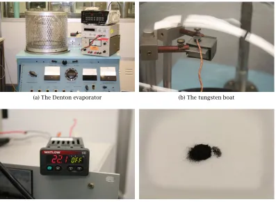
3.2 The Denton evaporator system. . . 38
3.3 The band diagram of petacene and Au. . . 40
3.5 The band diagram of the pentacene-Au interface [3]. . . 43
3.6 Illustration of the band diagram of polycrystalline material [4] . . . 45
3.7 µef f/µG versusLG. . . 46
3.8 Illustration of the in-house design. . . 46
3.9 The illustrated process flow of the in-house thin film pentacene transistor. . . 47
3.10 The thin film pentacene transitor film. . . 50
3.11 Drain and gate characteristics of the thin film pentacene transistors. . . 51
3.12 Illustration of the simplified transistor design. (a) silicon gate + silicon oxide gate insulator + bottom contact. (b) silicon gate + silicon oxide gate insulator + top contact. (c) metal gate + polymer gate insulator + bottom contact. (d) metal gate + polymer gate insulator + top contact. . . 52
3.13 Pentacene TFT with difference source/drain contact area. From top to bottom: 4mm×2mm, 4mm×0.5mm, 1mm×1mm, 1mm×4mm, and 1mm×0.5mm. . . 55
3.14 Testing structures for contact resistance measurement. . . 57
3.15 Pentacene mobilities after post-process annealing. . . 61
3.16 Mobilities of pentacene transistors on oxide after post-process annealing at 180◦C. 62 3.17 Comparison of pentacene transistor films as fabricated and annealed for 8 hours. 62 3.18 Illustration of KMnO4 reaction and the surface of Parylene C.. . . 63
3.19 SPM images of pentene on Parylene surfaces treated with KMnO4 and OTS. . . 65
3.20 SPM images of pentacene on As-deposited Parylene and oxide. . . 66
3.21 SPM images of as-deposited Parylene C. . . 67
3.22 SPM image of an oxide wafer. It is beyond the resolution of the SPM. . . 68
3.23 Surface roughness versus film thickness of as-deposited Parylene C. . . 68
3.24 Surface roughness of 5µm Parylene C after annealing at 180◦C. . . . . 69
3.25 Surface roughness of 10µm Parylene C after annealing at 200◦C.. . . . 69
3.26 Surface roughness of 1µm Parylene C after annealing at 200◦C. . . 70
3.28 SPM images of pentacene on Flip-Parylene. . . 73
3.29 SPM images of pentacene on Parylene surface smoothed with spin-cast dielectrics. 75 3.30 Parylene mechanical mask and the illustrated process. . . 78
3.38 Pentacene grain diameter versus channel lengths and metal types. (Negative values correspond to “away” positions.). . . 87
3.39 Pentacene grain diameter across the ring made of different metals. . . 88
3.40 Metal corrosion in saline solution. . . 90
3.41 The thin film pentacene transistors immersed in saline solution.. . . 91
3.42 Evolution of the field effect mobility of thin film pentacene transistors soaking in room-temperature saline solution. 1-µm parylene C protection. . . 92
3.43 Evolution of the field effect mobility of thin film pentacene transistors soaking in room-temperature saline solution. 10-µm parylene C protection. . . 93
3.44 Evolution of the field effect mobility of thin film pentacene transistors soaking in room-temperature saline solution. 20-µm parylene C protection. . . 93
4.1 Illustration of a solid under bending moment. . . 96
4.2 Two arcs with radii of curvature of 20×differences . . . 97
4.3 Bending of a silicon chip and thin film amorphous silicon.. . . 98
4.5 EDS spectrum of amorphous silicon on the oxide wafer, made out of 5 % silane
diluted in nitrogen. . . 102
4.6 EDS spectrum of amorphous silicon on the silicon wafer, made out of pure silane. 102
4.7 The drain and gate characteristics of undoped thin film amorphous silicon
transis-tor on oxide. . . 106
4.8 Cracks of Parylene N and D after 250◦C PECVD processes. . . . 108
4.9 the gate characteristics and drain characteristics of the thin-film transistor with
gate dielectric of amorphous silicon nitride.. . . 108
4.10 Delimination and bubbles of Parylene HT® on oxide immediately after Parylene
deposition. . . 110
4.11 Surface potential of Parylene HT®after the 310◦C PECVD nitride process. . . 111
4.12 The thin film amorphous silicon transistor, lifted off with SF6 sacrificial layer. . . . 113
4.13 Delimination after soaking in ATMI ST-22 120◦C. . . 114
4.14 The transistor film, manually lifted off without sacrificial layers.. . . 115
4.15 The HNA-released thin film amorphous silicon transistors. . . 116
4.16 the gate characteristics and drain characteristics of the HNA-released thin film
amorphous silicon transistors. . . 116
4.17 Illustrated process flow of the thin film amorphous silicon transistors.. . . 118
4.18 The thin film amorphous silicon transistor. . . 121
4.19 The drain and gate characteristics of the thin film amorphous silicon transistor.. . 122
4.20 The broken film due to compressive stresses. . . 123
4.21 Distribution of time-average potential of the capacitively-coupled planar RF PECVD
system. . . 124
4.22 Magnification of part of the drain characteristics of Figure 4.19. . . 125
4.23 The gate characteristics of transistors with near zero threshold voltages. (Modified
4.24 The gate characteristics of transistors with different threshold voltages. The red
curve is the original gate curve and the blue curve is the shifted one. . . 126
4.25 The thin film amorphous silicon immersed in saline solution. . . 129
4.26 Mobility and threshold voltage of thin film amorphous silicon transistors in saline
at room temperature (10µm Parylene C). . . 130
4.27 Mobility and threshold voltage of thin film amorphous silicon transistors in saline
at room temperature (20µm Parylene C). . . 130
4.28 Mobility and threshold voltage of thin film amorphous silicon transistors in saline
at room temperature (30µm Parylene C). . . 131
4.29 Mobility and threshold voltage of thin film amorphous silicon transistors in saline
at 80◦C (10µm Parylene C). . . 131
4.30 Mobility and threshold voltage of thin film amorphous silicon transistors in saline
at 80◦C (20µm Parylene C). . . . 132
4.31 Mobility of thin film amorphous silicon transistors in saline at 80◦C (30µm Parylene
C). . . 133
4.32 The drain and gate characteristics of the “failed” thin film amorphous silicon
tran-sistor after 3 days of soaking in 80◦C saline. . . . 133
4.33 The optical microscopic images of the corroded metal junction. . . 134
4.34 The SEM images of the surface of the Parylene covering the corroded metal junction. 134
4.35 The thin film amorphous silicon transistors with Parylene-Pt-Parylene encapsulation.134
4.36 Mobility and threshold voltage of thin film amorphous silicon transistors in saline
at 80◦C (5µm Parylene C, 1000 Å Pt, and 5µm Parylene C). . . . 135
5.1 The drain and gate characteristics of the thin film pentacene transistor and the
thin film amorphous silicon transistor. . . 140
5.2 The transfer curve of the inverter made of thin film pentacene transistor and thin
A.1 Illustration of a pattern transferring process using both positive and negative
pho-toresists.. . . 144
A.2 Weigth changes of AZ4903 photoresist versus soft baking time, courtesy of Mr. Chun-Hui Lin at the Caltech Micromachining Lab. . . 146
A.3 Anisotropic wet etching of silicon (<100>and<110>surfaces). . . 150
B.1 Four commercially available Parylene variants. . . 157
B.2 The Parylene coating equipment.. . . 157
B.3 Illustration of the Parylene deposition process.. . . 158
B.4 Parylene microfluidic devices. . . 160
B.5 The surface potential perµm of Parylene HT®. . . . 162
B.6 Temporal change of surface potentials of Parylene HT®samples with different an-nealing treatment. . . 164
B.7 Thermally stimulated discharge (TSD) measurement of Parylene HT®samples. . . . 165
B.8 Common design of micro electret power generators. . . 165
B.9 New design of micro electret power generators. . . 167
B.10 Illustrated mechanism of power generation.. . . 167
B.11 The power generator with metal rotors. . . 168
B.12 The surface potential of Parylene HT® coated on PEEK rotor blocks. There are 8 PEEK blocks in the figure and one block is identified with a black rectangle frame.. 169
B.13 The power generator with PEEK rotors. . . 169
B.14 The output power of the power generator with metal rotors. . . 170
List of Tables
2.1 Properties of silicon materials for thin-film transistors [1]. . . 23
2.2 Properties of the thin-film transistor made of N, N’-ditridecyl-3,4,9,10-perylene
tetracarboxylic diimide. . . 29
2.3 Properties of flexible substrates for thin film transistors. . . 31
3.1 Mobilities of thin film pentacene transistors with different source/drain area (cm2/Vs). 56
3.2 Contact resistance between Au/Cr and pentacene. . . 57
3.3 Hole mobilities of pentacene transistors with different source/drain contacts. . . . 59
3.4 Properties of pentacene transistors on oxide with different substrate temperatures
during deposition (W/L=1000/20).. . . 59
3.5 Contact angles of parylene surfaces after various treatments.. . . 64
3.6 Surface roughness of Parylene C after annealing at 200◦C.. . . . 70
3.7 Surface roughness of Parylene C smoothed with various spin-cast dielectrics. . . . 74
3.8 Properties of thin film pentacene transistors using smoothing layers and top/bottom
contact configurations. . . 80
3.9 Properties of top/bottom contact pentacene transistors on oxide (W/L=4000/20). . 81
4.1 Radii of curvature of silicon. . . 97
4.2 Properties of device-quality a-Si:H.. . . 99
4.3 Properties of device-quality SiNx:H. . . 100
4.4 Content of amorphous silicon on the oxide wafer, made out of 5 % silane diluted
4.5 Content of amorphous silicon on the silicon and oxide wafer, made of pure silane. 103 4.6 Properties of the undoped thin film amorphous silicon transistor.. . . 105 4.7 Electron field effect mobilities of thin film amorphous silicon transistors with
Pary-lene as gate dielectrics.. . . 107 4.8 Properties of the thin-film transistor with gate dielectric of amorphous silicon
ni-tride. . . 109 4.9 Process isolation: The PECVD processes make it impossible to release the Parylene
HT®with metal sacrificial layers. . . 111 4.10 Properties of the HNA-released thin film amorphous silicon transistors. . . 117 4.11 Properties of the thin film amorphous silicon transistor. . . 122
A.1 Properties of CVD processes. . . 154
B.1 Properties of Parylene N, C, D, and HT®. (Modified from courtesy of Dr. Siyang
Chapter 1
Introduction to Implantable Electronic
Systems
“He has an iron hook instead of a right hand, and he claws with it.” “Claws!”
“I say, John,” said Peter.
J.M. Barrie, “Peter Pan: Come Away, Come Away”
A medical prosthesis is an artificial extension that replaces a missing body part. Perhaps the most famous medical prosthesis is the shining hook of Captain Hook inPeter Pan. Prostheses are typically used to replace body parts lost by injury, or missing from birth or to supplement defective body parts. With the advance of technology, the medical prostheses have evolved from a simple but scary hook to a complex, computer-aided, and thought-controlled biomimetic microelectronic system.
1.1
Medical Diseases and Implantable Electronic Systems
Today, a variety of diseases can be treated with implantable electronic systems such as artifi-cial pacemaker, cochlear implants, cortical and spinal implants. These small electronic devices have greatly shaped our society as those consumer electronics. For some of the diseases, the implantable devices are the only cures available and for others, the implantable devices can help patients resume their daily life. The need for implantable devices is urgent and great. For example, according to the American Heart Association, an estimated 80,700,000 Ameri-can adults (1 in 3) have one or more types of cardiovascular diseases. The estimated direct and indirect cost of cardiovascular diseases is $448.5 billion. Among these cardiovascular dis-eases, artificial pacemakers and implantable cardiac defibrillators (ICD) are currently the only cures for certain types of arrhythmia (irregular heartbeat). In 2005, 91,000 implantable cardiac defibrillators procedures and 180,000 pacemaker procedures were performed in the United States.
In addition to cardiac implants, cortical and spinal implants also have great influences. According to the National Spinal Cord Injury Statistical Center (Birmingham, Alabama), the number of people in the United States who are alive in 2007 and have spinal cord injury has been estimated to be approximately 255,702 and approximately 12,000 new cases occur each year. The average health care and living expenses per year for a patient with spinal cord injury ranges from $228,556 to $775,567 for the first year and $16,018 to $138,923 for each subsequent year. Neural implants can benefit these patients. Sacral nerve stimulators now help patients with paraplegia control their bladders. The brain-computer interfaces, or cortical and spinal implants combined with external equipment like robots and motors, can help these paralyzed patient live an independent life and thus reduce their reliance on other people and save huge healthcare expenses.
Conventional implants such as pacemaker are based on technologies that are invented more than 50 years ago. The electronics of these implants are housed in hermetically-sealed metal cases (mainly titanium). Because of this metal housing, these implants have large form fac-tors. A typical pacemaker is approximately 40 mm by 40 mm by 8 mm. They are okay for subcutaneous implantations. However, there isn’t enough room at certain locations. Retinal implants resides inside the eye and the eye has only a volume of 6 mL. The spinal canal that houses the spinal cord is only 11.5 mm in diameter. Small and flexible implantable systems are required for implantations at such regions. Not only small dimensions, flexibility is also needed for these implants. A flexible implant can reduce the size of the implantation incision and thus shorten the scar healing time and in some cases, only a small area is available for surgical insertion of such implants.
In addition, multi-electrode arrays are also desirable. The maximum number of electrodes of current implantable devices is 22 of the cochlear implants. Retinal implants requires at least 64×64 electrodes and the neuroprobes for cortical implants need more than 96 electrodes.
Small dimensions, flexibility and capability of multi-electrodes are a few new features that advanced neural implants need. Others properties such as better encapsulations, low power consumption, complex logics and high computing speed are also among the features of ad-vanced neural implants.
1.2
The State of the Art
Today, there are a variety of implantable electronic systems in our daily life, including artificial pacemakers, cochlear implants, and neural prosthesis and retinal prosthesis. A brief sum-mary is given about artificial pacemakers, cochlear implants, and neural prosthesis and retinal prosthesis in the following section.
1.2.1
Artificial Pacemakers
A pacemaker or artificial pacemaker, is an electronic device that regulates the beating of the heart by stimulating the heart muscles with electrical pulses through the contact electrodes placed on the heart. The primary purpose of a pacemaker is to replace the malfunctioning native pacemaker of the heart.
Modern pacemakers are versatile. Cardiologists can externally program the pacemaker to suit individual patient’s need. Some pacemaker systems combine a pacemaker and implantable defibrillator in a single implantable package. Some have multiple electrodes that can stimulate different positions of the heart to improve synchronization of all the heart muscles.
As early as 1889, McWilliam reported the results of stimulation of the human heart with electrical pulses [6]. Ventricular contractions were sucessfully elicited by stimulation of elec-trical pulses and a stable heart rhythm of 60 – 70 beats per minute was also demonstrated. McWilliam opened the door to the development of the artificial pacemakers. In 1932, Albert Hyman invented an electro-mechanical device dubbed as “artificial pacemaker”. The term, “ar-tificial pacemakers” has come into use since.
muscle. In 1958, a fully-implantable pacemaker was first implanted into a human body.
At that time, the main concern of the development of the pacemakers was the continuous power supply. In early days, mechanical powering systems like springs were used. Later, pacemakers were powered by the short-life mercury batteries. In the late 1960s, nuclear battery powered pacemakers were developed. Not long, nuclear batteries were replaced by the lithium ion batteries. Wilson Greatbatch developed the first pacemaker powered by the lithium-iodide battery, which became today’s standard design of pacemakers.
Another concern of the pacemaker development is how to protect the implanted system from corrosion. In early days, the pacemakers are encapsulated with epoxy resins and water of the body fluid can easily permeate through the epoxy resins. Telectronics of Australia in 1964 provided a solution to this problem. They developed a pacemaker that was housed within a hermetically sealed titanium case. The pacemaker was encapsulated in epoxy with a final dip coat of a mix of epoxy and titanium dioxide. 1974, Cowdery developed pacemakers contained in a titanium cases welded with tungsten-inert gas (TIG) welding process. Laser-welding processes were also developing in late 1980s.
A typical internal pacemaker has dimensions of 42 mm by 42 mm by 8 mm and comes with a electrode measuring between 50 and 60 cm long. The system consists of a power source, usually a lithium cell, a sensing circuitry to capture natural heart beats and computer logics that controls the pacing device, output circuity delivering electrical pulses to the electrodes, and electrodes that contacts the heart muscles.
A pacemaker is typically implanted below the subcutaneous fat at the chest wall and above the muscles and bones of the chest via an incision made in the left shoulder area below the collar bone. The stimulating leads are fed into the heart through a large vein.
1.2.2
Cochlear Implants
system. The external system includes a microphone, a speech processor and n transmitter. The internal system contains a receiver and stimulator and a multi-electrode array.
Going back to the eighteenth century, Alessandro Volta, the developer of batteries, reported to hear sounds after stimulation of his own ears with a 50-volt circuitry. This is probably the first record of stimulation of the audio system with electrical pulses. In the 1950s, two French doctors, Djourno and Eyries, reported direct stimulation of an acoustic nerve. In the 1970s, Graeme Clark of University of Melbourne developed multi-channel cochlear implant sys-tems that stimulate cochlea at different positions. Successful implantations of multi-channel cochlear systems have been reported since 1978.
The cochlear implants are based on the tonotopic organization, or frequency-to-place map-ping, of the basilar membrane of the inner ear. Sounds are received by the microphone and processed by the speech processor. The transmitter sends out the processed sound signals via radio frequency electromagnetic wavers. The internal receiver and stimulator receives the transmitted signals and output electrical current pulses to the cochlea via the electrode array.
The electrode array is made of a special type of silicone rubber with platinum electrodes. One end of the electrode array is connected to the receiver/stimulator while the other end is extended into the cochlea. There are twenty-two electrodes on the multi-electrode arrays. Two electrodes sit outside the cochlea and function as ground electrodes: one is the ball electrodes that is placed underneath the skin and the other is a plate on the device.
The device is surgically implanted. A small incision is cut in the skin behind the ear and a hole is drilled on the skull into the mastoid bone and the inner ear. The electrode array is inserted into the cochlea.
By now, nearly 100,000 people worldwide have received cochlear implants.
1.2.3
Cortical Implants
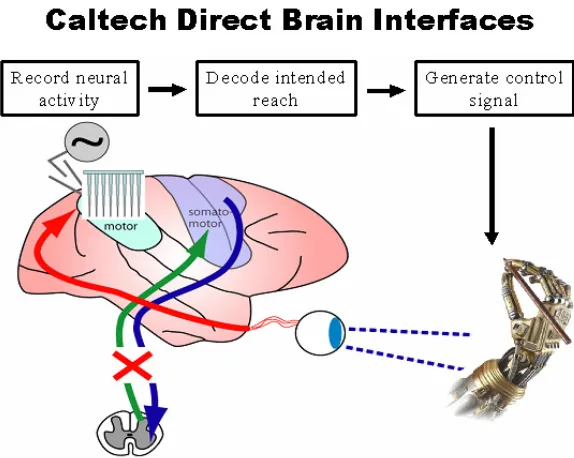
illustrates a system of cortical implants. Cortical implant systems can directly benefit those patients with spinal cord damages, peripheral nerve disease and amyotrophic lateral sclerosis (ALS, also known as Lou Gehrig’s disease). In the United States, more than two million people suffer from some forms of paralysis.
The Caltech researchers, Andersen, Tai and others, developed a direct brain interface system that use high-level cognitive signals for controlling external prosthesis equipment. This system directly records the cortex signals when the subject is thinking of something, interprets the signals and send controlling signals to the controlled equipment.
Figure 1.1: The Caltech direct brain interface. Courtesy of Dr. Changlin Pang.
1.3
Retinal Prosthesis: A Special Problem
Among all these electronic prosthetic implantations, the retinal prosthesis is a special sub-ject that posts additional challenges and constraints on the development of the implantable solution.
1.3.1
The Eye and Retinal Diseases
Vision occurs when the light enters the eye through the cornea and the pupil, is focused by the transparent crystalline lens, traverses the vitreous cavity of the posterior segment and finally hits the retina. At the retina, photoreceptors are activated by the incident photons and produce electrical signals that are carried to the visual cortex of the brain.
Because vision is created via a complex process signal transduction and transmission that requires the cooperation of numerous tissues and cells, the chances are high to break the process and blindness occur. Common blindness diseases includes cataracts, glaucoma, age-related macular degeneration (AMD), trachoma, cornea opacity and diabetic retinopathy. Some of these diseases result from blocking of the pathway of light to the retina, such as cataract, the disease of opacification of the lens. Some stem from loss of the retina’s capability of converting light into electrical signals or some barriers to the transmission of the converted electrical signals to the visual cortex, for example optical nerve damage from glaucoma. In addition to the drug treatment and surgical operations, implantation of electronic systems can cure some blindness diseases and even restore the patient’s damaged vision.
1.3.2
Electronic Implants in the Eye
signals on both the normal eye and the eye with outer retinal degeneration. This directed later interdisciplinary researches of medicine and MEMS to the field of ophthalmology. Later, the very same group led by Humayun demonstrated that visual responses could also be elicit by stimulating the retina with electrical signals [7].
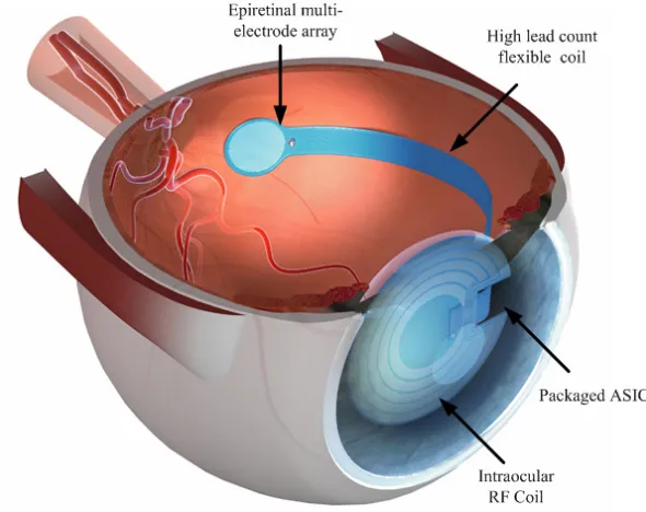
Based on the concept of direct stimulation of retina, a complete implantation system is proposed as the treatment solution. Figure 1.2 illustrates the intraocular system of retina prothesis. In this system, an external camera captures the vision of the patient and sends the encoded signals to the intraocular system. The radio frequency coil of the intraocular system receives the data and the power. The silicon chip packaged within the system is powered by the RF coil and processes data received by the RF coil. The chip then sends out electrical signals to the corresponding electrodes via a flexible cable.
Figure 1.2: The intraocular system of retinal prothesis. Courtesy of Dr. Damien Rodger.
Figure 1.3: The chip-level integrated interconnect (CL-I2) technology. Courtesy of Dr. Damien Rodger.
1.3.3
Limited Space in the Eye
This intraocular system is implanted inside the eye via surgical operations. As can been seen, the limited space in the eye places an additional contraint on the development of such in-traocular systems. The dimensions of the eye vary only 1 – 2 mm among humans. The vertical diameter is 24 mm and the transverse is a little bit larger. The total volume of the eye is roughly 6.5 mL. Within such a small space, implants with huge and cumbersome metal cases are not possible. Meanwhile, the system is recommended to have a width of approximate 2 mm for the ease of surgical insertion. Eye incisions less than 2 mm long can readily self-healed without any sutures. How to protect the implant electronic systems with constraints of small dimensions is a challenge to the existing MEMS technologies.
1.4
Technology Challenges
1.4.1
Corrosive Physiological Environment
the lens and the cornea. The aqueous humor is mainly composed of water (99%), ions (Cl−, Na+, K+, Ca2+, PO3−4 , etc.), proteins (albumin,β-globulin), ascorbate, glucose, lactate and amino acids. The vitreous humor mainly consists of water (99%), salts, sugars, vitrosin, a network of collagen type II fibers and mucopolysaccharide hyaluronic acid. Among these compositions, water, oxygen and chloride ions are usually considered the culprits of corrosions of silicon and metal.
In addition to corrosions of the implants caused by the body fluids, the implant can elicit immune responses of the body, too. Silicon implanted on the cortical surface of the rat brain causes significantly elevated tissue and glial cell reactions [9]. Accordingly, it is mandatory that silicon be covered with some sort of protective and biocompatible coating if silicon is to be used in implantable systems.
1.4.2
Mechanical Bending And Stress Concentration
One major problem that the aforementioned devices do not address is the stress-caused dam-age when the devices are bent. During surgical implantation operations, the retina prosthetic devices are folded and bent to fit into the small incisions. Other implants such as spinal cord implants may be bent and under torsion after being implanted inside the subject’s body. While the retina prosthetic devices based on Parylene are flexible, some points on the device may be the stress concentration points when the device is bent.
The retina prosthetic device is mainly a silicon chip encapsulated with Parylene and thus can be treated as a Parylene-silicon-Parylene sandwiched structure. This sandwiched structure can be modeled as a composite beam problem. The bending of the composite beam is can be analyzed via the following partial differential equations:
The moment-curvature relationship:
whereMis the bending moment,κis the curvature, theEP aandIP aare the Young’s Modulus and moment of inertia of Parylene, andESi andISi are the Young’s Modulus and moment of inertia of silicon.
and the bending stress, or the flexural stress, is given by:
σx= −
My
I . (1.3)
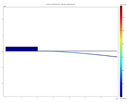
As is the case of usual mechanical problems, this bending problem is too complicated and has no closed-form solutions. The computer software, COMSOL Multiphysics® is employed to solve the problem. Because of symmetry, the bending problem is modeled a composite beam with sandwiched material, which is fixed at one end and free at the other, as shown in Figure1.5.
Figure 1.4: Illustration of The bending problem.
The thickness of the silicon chip ranges from 0.5 to 250µm and it is 2.5 mm long. Both the substrate and top Parylene C are 10µm thick. Figure1.6shows the stress inside the Parylene-silicon-Parylene structures. As the thickness of silicon reduces, the high stress area moves from the edge of the silicon chip to the fixed end of the beam and the high stress area switch from Parylene to silicon chip.
Figure 1.5: The bending problem.
(a) 250µm silicon (b) 10µm silicon
(c) 1µm silicon (d) 0.5µm silicon
the failure of Parylene while for thin-film transistor technology, it is the brittle silicon thin film that causes the mechanical failure.
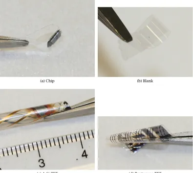
A Parylene C film with a 250 µm silicon chip packaged inside is used for the mechanical bending test. After several bendings, the Parylene C film shows permanent deformation at the edges of the silicon chip. The Parylene surface shows clear cracks, as can be seen in the SEM images, Figure1.7. Such cracks could lead to starting points of corrosion and increased water permeation. As a comparision, a blank Parylene C film, a Parylene C film with amorphous silicon transistors and a Parylene C film with pentacene transistors also undergo the same tests. Figure1.8shows these films after the bending test.
(a) The surface covering the whole chip (b) The crack
Figure 1.7: The SEM images of Parylene C film with a silicon chip inside after the mechanical bending test.
1.5
The Goal and Scope of This Study
(a) Chip (b) Blank
(c) A-Si TFT (d) Pentacene TFT
Chapter 2
Thin-Film Electronics Approaches
2.1
Introduction
Although thin-film transistors seem new and novel in application of bio-implants, they are the building blocks of today’s display industry. Recognized by Brody [10], Heil presented the first concept of the thin-film transistor in his 1935 British patent [11]. The first working thin-film transistor was demonstrated by Weimer [12]. His thin-film transistor is composed of micro-crystalline cadmium sulfide, CdS, as the semiconducting material, silicon oxide as the gate insulating dielectrics and gold as metal for source/drain contacts and interconnects. Since then, numerous researches on thin-film transistors have emerged. In the beginning, the target application and market of the thin-film transistor technology was the VLSI application. How-ever, due to low mobilities and other poor device parameters and mainly the fast development of bulk silicon electronics, the thin-film transistor technology yield its place to single crystal MOSFET technology.
However, the thin-fim transistor technology revived in a new application, the display area. Brodyet al. demonstrated the first active matrix LCD (AMLCD) based on CdSe thin-film tran-sisotrs and the nematic liquid crystal [13].
successful doping of hydrogenated amorphous silicon. Spear and Le Comber et al. reported successful doping of amorphous silicon with mixture of phosphine/diborane and silane [14][15] and subsequently fabricated the first a-Si:H thin-film transistors [15].
It is the commercial market of TFT LCD that spurs the development of thin-film transistors. According to iSuppli Corp., the global revenue for large-sized LCD panels, or those with diagonal dimensions of 10 inches or greater, rose up to $66 billion in 2007, up 22.2 percent from $54 billion in 2006. The rising trend will continue in the coming years. The large-sized LDC panel market will expand to 597.6 million units by 2011 and the revenue will reach $102 billion in 2011.
As is the case of other multidisciplinary researches, this research of bio-implantable elec-tronics borrows the thin-film transistor technology from the display industry.
2.2
Design of Thin-Film Transistors
There are ohmic contact layers between the source/drain electrodes and the semiconductor layer. The ohmic contact layers are to form ohmic contacts between the source/drain elec-trodes and the semiconductor and to reduce contact resistance. For silicon thin-film transistors, heavily-doped n+ or p+ silicon is used as the ohmic contact layers. For organic thin-film tran-sistors, the ohmic contact layers are omitted. Instead, ohmic contact between the source/drain electrodes and the semiconductor is achieved througth proper selection of the metal type used as the soruce/drain electrodes. Generally, metals with work functions higher than 4.3 eV can form good contact with pentacene.
(a) Staggered (b) Coplanar
(c) Inverted Staggered (d) Inverted Coplanar
Figure 2.1: Common structures of thin-film transistors.
2.3
Thin-Film Semiconducting Materials
2.3.1
Inorganic Semiconductors
2.3.1.1 Silicon
Silicon has long been used in microelectronics. From a chip in a cell phone to a RFID in a baggage, silicon is everywhere in our daily life. However, silicon used in thin-film transistors is different from its siblings in VLSI industry.
ma-terial used in applications of large-area electronics, for example flat-panel displays. In addition to amorphous silicon, silicon with other degrees of crystallinity can also be used for thin-film transistors. However, the research on semiconducting materials of thin-film transistors de-pends on mobility/grain sizes and process temperatures.
Silicon of various degrees of crystallinity can be either directly deposited on the substrates or be obtained from crystallization of amorphous silicon precursors. Generally, films of sili-con are divided into four categories: amorphous silisili-con (a-Si), nanocrystalline silisili-con (nc-Si), microcrystalline silicon (µc-Si), and polycrystalline silicon (pc-Si). The mobility increases with grain sizes in general because grain boundaries are usually the sites of trapping and scatter-ing for movscatter-ing charge carriers. Figure2.2summarizes the mobilities, process temperatures, applications, and deposition methods of silicon with various degrees of crystallinity.
Amorphous Silicon The baseline deposition process of amorphous silicon is the radio fre-quency plasma-enhanced chemical vapor deposition (RF-PECVD). It is the most common depo-sition process to obtain amorphous silicon. The common process temperature is 250–300◦C. Typical electron field mobility of hydrogenated amorphous silicon is around 0.5 cm2/Vs.
One of the advantages of RF-PECVD is that it is easy to lower the process temperatures from 250 – 300◦C to temperatures lower than 150◦C for flexible polymer substrates. Quality of amorphous silicon deposited at lower temperatures can be amended by increasing hydrogen content [16][17][18]. Similarly, the silicon nitride deposited with PECVD processes can also be deposited at lower temperatures with hydrogen enhancement. The source gases, such as silane, nitrogen and ammonia, are usually diluted in hydrogen for low-temperature processes. Amor-phous silicon and nanocrystalline silicon deposited at lower temperature show comparable field mobility as deposited at typical temperatures [19][20][21][22].
Figure 2.2: Properties of silicon with various grain sizes [1][2].
Abbreivation:
RF-PECVD: radio frequency plasma-enhanced chemical vapor deposition
ECR-PECVD: electron cyclotron resonance plasma-enhanced chemical vapor depositio HW-CVD: hot-wire chemical vapor deposition
SPC: solid phase crystallization MIC: metal-induced crystallization ELA: excimer laser annealing
Nanocrystalline Silicon Nanocrystalline silicon (nc-Si) and hydrogenated amorphous silicon (a-Si:H) can be obtained by the same deposition process. A typical process temperatures of PECVD nc-Si is 250 – 300◦C. With hydrogen dilution of the source gases, the process tempera-ture can be lowered, as is the case of amorphous silicon. Nanocrystalline silicon deposited at 150◦C by PECVD processes shows mobility of 40 cm2/Vs [25]. Higher electron mobility up to 450 cm2/Vs has also been demonstrated [26].
Mirocystalline and Polycrystalline Silicon Microcrystalline and polycrystalline silicon can be obtained by directly deposition or deposition of precursors followed by crystallization. Direct deposition of microcrystlline and polycrystalline silicon is usually done by low-temperature chemical vapor deposition (LPCVD). The typical processing temperature of LPCVD silicon is 600◦C. Likewise, such high process temperatures prevent fabrication of thin-film transistors on polymer substrates and glass substrates.
crystal-lization process is usually done by solid-phase crystalcrystal-lization (SPC), metal-induced crystalliza-tion (MIC) or excimer laser annealing (ELA).
Solid phase crystallization (SPC) is a common method to obtain polycrystalline silicon from amorphous silicon. Amorphous silicon is a noncrystalline elemental solid and is considered to be at a metastable state. When amorphous silicon is annealed at high enough temeprature, the phase transformation from amorphous state to crystalline state takes place by a thermody-namic driving force. The transformation is typically carrried out with a simple furnace anneal-ing at around 600◦C. It can also be done through a rapid-thermal annealing system at a higher temperature but shorter time. Thin-film transistors made of n-type pc-Si obtained through 650 ◦C annealing exhibit mobility of 64 cm2/Vs [27]. However, the SPC annealing temperature is
too high for flexible polymeric substrates.
Metal-induced crystallization (MIC) is a metal-induced transformation of amorphous silicon into crystalline silicon. Silicide, or Si-metal alloys are common materials in VLSI circuits. It is well known that the interactions between some metals, such as Al and Au, and amorphous silicon induce the crystallization of amorphous silicon at temperatures much lower than those of SPC processes. Though the kinetics of such a low temperature crystallization process has not been established, most of the experimental data show that addition of a small amount of metal impurities can dramatically enhance the crystallization of amorphous silicon at low temperatures. The reaction between a metal and amorphous silicon occurs at the interface and it lowers the crystallization temperature. Metal used as contact layers in metal/a-Si structures can be classified into two groups: silicide forming metals (Ni [28][29], Co, Cr, Pd [30], and Pt) and elemental metals that do not form silicides (Al [31][32], Ag, Au [33][34], and Sb). Thin-film transistors made of pc-Si crystallized via MIC processes show electron mobility of 121 cm2/Vs [28].
into polycrystalline silicon via laser annealing. By selectively deposit very large amounts of en-ergy in the near-surface region of amorphous silicon in a very short time, pulsed excimer laser annealing shift the maximal process temperature from the crystallization step to other process-ing steps. Thin-film transistors made of polycrystalline silicon crystallized via ELA processes show electron mobility of 120 cm2/Vs [35]. The development of excimer laser annealing per-mits fabrication of polycrystalline silicon thin-film transistors on low-temperature polymeric substrates such as PET and PEN [36][37].
Table2.1summarizes silicon materials for thin-film transistors.
Table 2.1: Properties of silicon materials for thin-film transistors [1].
Types of Silicon Films a-Si:H nc-Si:H µc-Si
Standard deposition temperature (◦C) 250 250 150-250 (precursor)
Highest process temperature (◦C) 350 280 crystallization
temperatures Steps with highest process nitride heavily doped n, p crystallization temperatures
Electron mobility (cm2V−1s−1) 0.5 – 1 40 300
Hole mobility (cm2 V−1s−1) 0.01 0.2 50
Conducitivity (S cm−1) 10−11 10−7 – 10−2 10−6
Growth rate (Å s−1) 1 – 10 1 1 – 10
Source/drain configuration Inverted staggered staggered, coplanar coplanar
Gate insulating dielectric nitride oxide oxide
2.3.1.2 Other Inorganic Semiconductors
Transparent Oxides III-VI compound oxides, such as ZnO and its derivatives, provide another school of semiconducting materials for thin-film transistor applications. Such oxides are gen-erally transparent and therefore allow unusual applications such as invisible electronics for head-up displays on windshields or cockpit enclosures. Such oxide films are usually obtained by room-temperature radio frequency magnetron sputtering and thus can be easily fabricated on flexible polymeric substrates. Thin-film transistors made of transparent ZnO exhibit elec-tron mobility of 27 cm2/Vs [38].
for thin-film transistors. Amorphous InGaO3(ZnO)5(a-IGZO) films with good properties can be formed on plastic substrates at room temperature [39]. The thin-film transistors with channel made of a-IGZO show electron mobility of 10 cm2/Vs, an order higher than a-Si:H thin-film transistors and organic thin-film transistors [39].
Transparent thin-film transistors made of transparent oxides and transparent conductors, for example indium tin oxide (ITO), can be applied in a range of applications, such as backplanes for backlit LCD’s and for some OLED’s.
A Few Others In addition to silicon and transparent oxides, other materials, such as CdS and CdSe, are also used as the channel material of thin-film transistors. In fact, the first thin-film transistor, made by Weimer, was fabricated with a thin film of polycrystalline CdS [12]. More-over, the first active-matrix liquid crystal display (AMLCD) had CdSe-based thin-film transistors as the pixel switch [13]. Not only on rigid substrates, CdS-based thin-film transistors has been fabricated on papers, Mylar®, Kapton® and other flexible substrates [40]. Unfortunately, the development of silicon-based electronics overturned the development of electronics based on chalcogenide compounds.
2.3.2
Organic Semiconductors
Organic semiconductor thin films can be deposited by physical vapor deposition. Heated up to the sublimation temperature, organic semiconductors are deposited in a variety of vacuum systems, such as organic molecular beam deposition (OMBD) systems, common bell-jar vacuum systems and simple glass-wall sublimation systems.
Organic semiconducting materials that can be deposited by PVD processes include: Cu-phthalocyanine [41][42][43],α-sexithiophene [44][45][46], pentacene [47] [48][49] and so on.
2.3.2.1 Pentacene
Pentacene is a polycyclic aromatic hydrocarbon consisting of 5 linearly-fused benzene rings. The extended conjugation and its crystal structures gives its semiconducting properties. How-ever, pentacene generates excitons upon absorption of ultra-violet or visible light and makes itself sensitive to oxidation. This puts a great challenge in pentacene-based long-term applica-tions.
Vapor-deposited pentacene-based thin-film transistors have been demonstrated with mobil-ities up to 3 cm2/Vs [47], and 3–4 cm2/Vs with surface treatments of self-assembly molecules and as high as 5 cm2/Vs with polymeric surface treatment [50]. Field effect mobilty of 35 cm2/Vs at room temperature was reported for purified single crystalline pentacene [51].
In addition to thin-film transistors, pentacene combined with buckminsterfullerene is used in applications of organic photovoltaic devices [52].
The solubility of organic semiconductors is the key factor for development of low-cost and large-area processing technologies, including spin-coating, inkjet printing and dip coating. But almost all small molecules are insoluble. A workaround method uses soluble precursors and later converts the precursors into the desired molecules via thermal processes. Pentacene has been fabricated in such a manner with mobilities ranging from 0.3 to 0.9 cm2/Vs [53].
processes to pattern pentacene films have been developed [54].
2.3.2.2 Other Organic Semiconductors
Polymers Most of the organic semiconducting polymers reported in literature are derivatives of thiophene. Because of high solubility, films of polymer organic semiconductors are often made with solution-based processes, like spin or drop casting. Although vapdeposited or-ganic semiconductors generally show better device performances, solution processed oror-ganic semiconductors have the potential for large-area and low-cost printing and rolling fabrication processes. Conventional photolithography and vacuum pumping systems can be eliminated with the use of soluble organic semiconductors. One of the first solution-processed organic semiconductors used in thin-film transistors is poly(3-hexylthiophene), or P3HT. The hexyl side chains may be replaced with other alkyl side chains without affecting the mobility much.
It is well known that performance of polymer thin-film transistors relies heavily on the chemical and structural order of the polymer [55]. Deposition of highly ordered polymer films depends on the regioregularity of the polymer and the molecular orientation on the substrate. The highest mobility of polymer thin-film transistors is 0.1–0.2 cm2/Vs [56].
Other thiophene derivatives are used for thin-film transistors. Paulet al. fabricated thin-film transistors based on poly(9,9’-dioctyl-fluorene-co-bithiophene) (F8T2) and regioregular poly(thiophene) with ink-jet printing technologies [57].
Small Molecules In addition to pentacene, another small molecule dominates the literature of organic thin-film transistors made of small molecules: oligothiophene.
Oligothiophenes, either unsubstituted ones from terthiophene (3T) to octithiophene 8T, or substituted by alkyl chains are well studied. These oligothiophenes are most often deposited via vacuum evaporation because of their very low solubility.
transistors with mobilities up to 0.5 cm2/Vs [59].
Single Crystals The reports on thin-film transistors made of single crystalline organic semi-conductors are rare. The major problem is the deposition of the single crystal semiconductor. Typical organic thin-film transistors are fabricated by depositing the semiconducting organics on a very flat gate insulating dielectric, either from vapor phase or by casting from a solution. Single crystal organics cannot be deposited this way. Carefully-controlled crystal growth is required for single crystal organics. Mobility of single crystal organics often suffers from the poor surface of the gate insulating dielectric. Thin-film transistors made of single crystalline sexithiophene show hole mobility of 0.075 cm2/Vs [60].
The problem mentioned above is solved by depositing the gate insulator on top of the single crystal. By incorporating Parylene C as the gate insulator and using a top-gated paradigm, thin-film transistors based on single crystal organics have been demonstrated to have mobilities up to 8 cm2/Vs for single crystal rubrene [61] and up to 0.3 cm2/Vs for single crystal pentacene [62].
N-type Organic Semiconductors For inorganic semiconductor materials, the polarity is de-termined by doping of impurities. However, the polarity of organic semiconductors can be determined by 2 factors. The first is the ease of conduction. That is, the organic material is called n-type if its electron mobility is substantially higher than its hole mobility and p-type vice versa. In fact, in OLED area, their properties are termed with electron/hole transport. The other is charge injection. A n-type organic semiconductor is a material in which electrons are easily injected, and a p-type holes. Rather than the doping impurities, the types of organic semiconductors depends on the work functions of metal contacts and electron affinity of the organic material [63].
Among them, N, N’-dialkyl-3,4,9,10-perylene tetracarboxylic diimide has been reported to have electron mobilities up to 0.6 cm2/Vs [65]. But N, N’-dialkyl-3,4,9,10-perylene tetracar-boxylic diimide is sensitive to oxygen and water and the mobility decays fast after fabrication of the transistors.
A top-contact thin-film transistors based on N, N’-ditridecyl-3,4,9,10-perylene tetracarboxylic diimide is made with silicon dioxide as the gate insulating dielectric. The organic semiconduc-tor film is deposited with the Denton evaporasemiconduc-tor under a pressure less than 1×10⁻⁶Torr. Au is used as the source and drain contact. Figure 2.3shows the SPM image of N, N’-ditridecyl-3,4,9,10-perylene tetracarboxylic diimide, Figure2.4shows the drain and gate characteristics of the thin-film transistor, and Table2.2summarizes the properties of this thin-film transistor.
(a) The drain characteristics (b) The gate characteristics
Figure 2.4: The drain and gate characteristics of the thin-film transistor made of N, N’-ditridecyl-3,4,9,10-perylene tetracarboxylic diimide.
Table 2.2: Properties of the thin-film transistor made of N, N’-ditridecyl-3,4,9,10-perylene tetracarboxylic diimide.
Gate Insulator 1245Å oxide
W/L 3000/60
Source/Drain 500Å Au
Electron Mobility 0.016 cm2/Vs
Threshold Voltage 33.38V
2.4
Flexible Substrates
Flexible thin-film transistors are recently under much of research and industry interests, espe-cially for applications of flexible displays. In TFT LCD display applications, a shift from glass substrates to flexible substrates is required in order to reduce the weight of the displays and produce flexible, conformal and rollable displays. Thin-film transistors have been fabricated on flexible substrates such as metal foils and polymer substrates. The deposition process of the semiconducting thin film seriously limits the choices of the flexible substrates. The most important factor of the deposition process is the maximal process temperature.
2.4.1
Metal Foils
The most common metal flexible substrate for thin-film transistors is steel foils. A widely-used and commercially available steel foil is American Iron and Steel Institute (AISI) Grade 304 stainless steel (Fe/Ni/Cr 72/18/10 wt.%). By tolerating temperatures of close to 1000◦C, steel substrates permit the adoption of many process used by the integrated circuit industry. Thus, all types of silicon thin-film transistors can be fabricated on steel foils. Polycrystalline silicon thin-film transistors have been fabricated on 200µm-thick steel substrates by Wu et al. with maximal process temperatures of 700◦C[67]. The achieved electron field effect mobility was 64 cm2/Vs. Maet al. fabricated amorphous silicon thin-film transistors on 3 – 200µmsteel foils with maximal process temperatures of 350◦C and achieved an electron field effect mobility of 0.6 cm2/Vs [68]. Chenet al. demonstrated a flexible amorphous silicon TFT active-matrix display on 300-µm steel foil [69]. But the drawbacks of steel foils are their opaqueness and large parasitic capacitance.
2.4.2
Polymer Substrates
Table 2.3: Properties of flexible substrates for thin film transistors.
Flexible Substrates Maximum Allowable Process Allowable Processes Temperature (◦C)
1Excimer laser annealing.2Spin-casting/thermal evaporation of organic semiconductors
solutions, thin-film transistors have been fabricated on polymeric substrates. Common poly-meric substrates are polyimide (PI), polyethylene naphthalate (PEN) and polyethylene tereph-thalate (PET). One major difference between metal foils and these polymeric films is the maxi-mal process temperatures the polymeric films can tolerate. Polyimide films, such as DuPont™ Kapton® has glass transition temperatures between 360 and 410◦C and thus are incapable of LPCVD processes. Instead, silicon-related PECVD processes are commonly applied to fabricate silicon thin-film transistors on polyimides [70]. However, polyimide films are opaque, yellow and thus have limited display-related applications. PEN and PET are both clear but with much lower temperature tolerances. DuPont™ Mylar® PET films have glass transistion temperature of 67 ◦C and DuPont™ Teonex® PEN films 120 ◦C. Silicon thin-film transistors are fabricated on these clear substrates with special low-temperatures PECVD processes [37][20] and room-temperature sputtering processes [71][72]. To no surprise, spin-cast or thermally evaporated organic semiconductors can be easily deposited onto the aforementioned polymeric substrates [73][74][49][75]. Table2.3lists some properties of common flexible substrates.
2.5
Parameter Extraction of Thin-film Transistors
The threshold voltage of a thin-film transistors is given by
VT=VF B+2ψB+ 2
Ci
q
sqNψB, (2.1)
whereVF B is the flat band voltage, qψB is the difference of the Fermi level and the intrinsic level of the semiconductor, N is the concentration of charge carriers ands is the permittivity of the semiconductor andCi is the capacitance of the gate insulating dielectric per unit area.
Ci can usually be expressed with the expressionCi =i/d, whereiis the permittivity of the gate insulating dielectric, anddis its thickness. But in reality,Ci is measured directly due to process variations.
The drain current under a certain drain voltage,VDand gate voltage,VG is given by
ID=µCi
For low drain voltages(VDS < VGS−VT), or the linear regime, Equation2.2can be simplied as
The conductance of the transistor in the linear regime is
g= ∂ID
∂VDS
' W
LµCi(VGS−VT). (2.4)
For drain voltages,(VDS ≥VGS −VT), or the saturation regime, the voltage across the gate insulator dielectric decreases near the drain and as a result, the channel becomes pinched off at the drain end and the current saturates. The saturation condition is given byVDS,sat.'VGS−VT. Thus, Equation2.2can be simplified to
The transconduction in the saturation regime can be obtained by differentiating Equation2.5
In real world, it is often the case that a transistor is fabricated and we have to extract all the parameters from direct measurement results of the device. The HP4145B semiconductor parameter analyzer is often used to measure transistor characteristics. There are two kinds of transistor characteristics plots. The output characteristics plot the drain current as a function of the drain bias with gate bias as a parameter (Figure 2.4). On the other hand, the transfer characteristics plot the output drain current as a function of the input gate bias, for fixed drain bias (Figure2.4).
To extract the carrier mobilityµ and the threshold voltageVT in the saturation region, we can plot the square root ofIDas a function ofVGS. By linear regression, we can get the threshold voltage from the intercept and and the mobility from the slope. By taking square root on both sides of Equation2.5, we have
Solving this equation and use a definition of “k” as
k=
Equating the linear regression slope of the plotp
IDversusVGto “k” determines the mobilityµ in the saturation regime. The threshold voltage can also be extracted from the same equation.
transistors, this is not a serious problem since thin-film transistors often have long channel lengths.
2.6
Discussions
Chapter 3
Thin-Film Pentacene for Implantable
Electronics
To develop flexible electronics for implantable applications, it is natural to look for electron-ics based on organic semiconductor since they are either polymers or small molecules and there is no problem bending these thin film organic semiconductors. This chapter discusses pentacene-based thin-film transistors for bio-implantable applications. The working principles behind the thin film pentacene transistors are presented and thin film pentacene transistors are developed. To have better devices performance, the process parameters, the properties of Parylene surfaces and the surface morphologies of pentacene are investigated in detail. Fi-nally, soaking tests of thin film pentacene transistors are carried out to evaluate bio-implant reliability of thin film pentacene transistors.
3.1
Material
3.1.1
Pentacene and Why It Is Selected
Pentacene is a polycyclic aromatic hydrocarbon consisting of 5 linearly-fused benzene rings. At room temperature, pentacene is in a form of purple-colored powders. Figure3.1illustrates the synthesis process of pentacene . The melting point of pentacene is greater than 300 ◦C and it sublimes at 372 – 374◦C. Because of oxidation, the color of pentacene powder slowly turns green after long exposure of air and light. Pentacene belongs to a family of linear acenes and its siblings include tetracene (four fused benzene rings) and hexacene (six fused benzene rings).
Figure 3.1: Synthesis of pentacene.
deposition or spin casting from precursor solutions followed by conversion reaction steps.
3.1.2
Deposition of Thin Film Pentacene
In general, thin film pentacene can be made by either depositing from vapor phase or casting from solution of precursors followed by synthesis reaction. Afzaliet al. described a reflow method to synthesize pentacene from its precursor solution [53] and Yamadaet al. demon-strated a photosynthesis process of pentacene from soluble precursors [76]. Casting from solution eliminates the need of sophisticated and expensive vacuum systems and thus reduces the cost of production. However, the devices made from solution casting show inferior perfor-mances to those made from vacuum deposition.
On the other hand, most of the best thin film pentacene transistors ever reported in liter-ature were made through vacuum deposition. One of the key factors of vacuum deposition that influence device performances is the base pressure. The lower the base pressure is, the lower, the chances of oxidation are and thus the better quality of the pentacene thin film is. It ranges from less than 10−9Torr of an organic molecular beam deposition system, to 10−7Torr of a common high-vacuum bell jar system and up to 10−3 Torr of an home-made simple vac-uum deposition system. In addition to direct physical vapor deposition, organic vapor phase deposition (OVPD), which consists of evaporating the molecular material into a stream of hot inert carrier gas that transports the vapors from the source to the cooled substrates where condensation of the organics occurs [77].
(a) The Denton evaporator (b) The tungsten boat
(c) The Watlow controller (d) Pentacene powder
3.2
Thin-Film Pentacene Transistors in Theory
A typical thin film pentacene transistor consists of a thin semiconductor film, a insulator layer, and the gate and source/drain electrodes. Though both are dubbed as thin-film transistors, thin film pentacene transistors do not behave in the same way as amorphous silicon thin-film transistors.
3.2.1
Hole Injection into Pentacene
Figure 3.3 illustrates the band diagrams of Au and the highest occupied molecular orbital (HOMO) and the lowest unoccupied molecular orbital (LUMO). When a positive voltage is applied on the gate electrode, negative charges builds up on the source electrodes. Because, the Fermi level of Au is far away from the LUMO level of pentacene, the electron injection into pentacene is very unlikey and thus, no current conduction occurs and the transistor is in the off state. On the other hand, when negative voltages are applied to the gate, positive charges accumulate on the source electrode and holes can be readily injected into pentacene because the Fermi level of gold is close to the HOMO level of pentacene. Thus, a conduction channel forms and charges can be driven from the source to the drain by a second bias applied between the source and the drain. Accordingly, pentacene is regarded as a p-type semiconductor. Unlike silicon, the n-type and p-type are determined by the impurity doping, the polarity of an organic semiconductor is determined by its HOMO/LUMO levels and the work function of the contact metal.
3.2.2
Thickness of Conduction Channel
The thickness of conduction channel of the thin film pentacene transistor plays an important role in understanding the thin film pentacene transistor and also determining the proper thick-ness of the souce/drain electrodes to reduce contact resistance.
Figure 3.3: The band diagram of petacene and Au.
The derivation starts from the one-dimension Poisson equation:
∂2ψ
∂x2 = −
ρ(x) s
, (3.1)
whereψis the potential at the position of distancex, normal to the insulator-semiconductor interface andρ(x)is the charge density ands is the permittivity of the semiconductor.
The charge density at the pointxcan be expressed in terms of the surface charge density at the insulator-semiconductor interface (x=0):
ρ(x)=qn0·e q(ψ−ψ0)
kT , (3.2)
whereψ0is the potential andqn0is charge density the at the insulator-semiconductor interface (x=0)
Combining Equation3.1and Equation3.2gives:
∂2ψ
∂x2 = −
qn0
<



![Figure 3.5: The band diagram of the pentacene-Au interface [3].](https://thumb-us.123doks.com/thumbv2/123dok_us/783155.1091281/65.612.227.426.141.324/figure-band-diagram-pentacene-au-interface.webp)
![Figure 3.6: Illustration of the band diagram of polycrystalline material [4] .](https://thumb-us.123doks.com/thumbv2/123dok_us/783155.1091281/67.612.218.431.250.453/figure-illustration-band-diagram-polycrystalline-material.webp)