Frequency of Semiconductor Lasers
Thesis by
Naresh Satyan
In Partial Fulfillment of the Requirements
for the Degree of
Doctor of Philosophy
California Institute of Technology
Pasadena, California
2011
© 2011
Naresh Satyan
Acknowledgements
I am grateful for the support, encouragement, and friendship of a large number of
people who have made my stay at Caltech productive and enjoyable.
I am thankful to Prof. Amnon Yariv for the opportunity to be a member of
his research group, and the freedom to grow as a researcher. He has always been a
source of inspiration with his intuition and insight, and being part of his group has
allowed me to interact with, and learn from, a number of knowledgeable and talented
individuals.
A large part of this work has been collaborative, and I thank the number of
re-searchers with whom I have benefited from working. Dr. Wei Liang was instrumental
in helping me develop a good understanding of the theoretical and experimental
as-pects of optical phase-locked loops. I have enjoyed numerous brainstorming sessions
with Dr. George Rakuljic, discussing new ideas and their feasibility and relevance
to the real world. I have learned much about experimental system design from Dr.
Anthony Kewitsch. More recently, I have enjoyed exploring various facets of
optoelec-tronic control with Arseny Vasilyev, Jacob Sendowski, and Yasha Vilenchik. I have
also had the pleasure of collaborating with other groups on some aspects of this work:
Firooz Aflatouni and Prof. Hossein Hashemi at the University of Southern California
designed custom integrated circuits to phase-lock semiconductor lasers; and Jason
Gamba and Prof. Richard Flagan at Caltech helped us demonstrate the feasibility of
using our laser sources for biomolecular sensing.
I thank the many current and past members of the research group with whom I
have had fruitful interactions. Dr. John Choi and I spent too many hours together
has provided stimulating conversations and expert advice every week. I have enjoyed
technical and other discussions with Prof. Bruno Crosignani, Prof. Joyce Poon, Prof.
Lin Zhu, Dr. Philip Chak, Prof. Avi Zadok, Dr. Xiankai Sun, Hsi-Chun Liu, Christos
Santis, Scott Steger, James Raftery and Sinan Zhao. I owe special thanks to Connie
Rodriguez for her thoughtfulness and hard work in looking after us. I also thank
Alireza Ghaffari, Kevin Cooper and Mabel Chik for their support.
I thank Profs. Bruno Crosignani, Ali Hajimiri, Kerry Vahala, and Changhuei
Yang for serving on my candidacy and thesis committees.
I am fortunate to have formed many friendships at Caltech that have helped me
ex-plore my interests outside work. Phanish Suryanarayana, Pinkesh Patel, Setu Mohta,
and Devdutt Marathe have been wonderful roommates. I have greatly enjoyed the
Carnatic music sessions with Shankar Kalyanaraman, Prabha Mandayam and Chithra
Krishnamurthy. John Choi and Philip Tsao have introduced me to bad movies and
good food. I have enjoyed many great times—on and off the cricket field—with the
large Indian contingent at Caltech: Tejaswi Navilarekallu, Abhishek Tiwari, Vijay
Na-traj, Sowmya Chandrasekar, Krish Subramaniam, Swaminathan Krishnan, Shaunak
Sen, Vikram Deshpande, Vikram Gavini, Abhishek Saha, Anu and Ashish Mahabal,
Sonali and Vaibhav Gadre, Mayank Bakshi, Mansi Kasliwal, Zeeshan Ahmed, Uday
Khankhoje, Ravi Teja Sukhavasi, Bharat Penmecha, Varun Bhalerao, Shriharsh
Ten-dulkar and Srivatsan Hulikal. Thanks to all my regular hiking partners over the years:
the Caltech Y, members of my research group, Shankar Kalyanaraman, Mayank
Bak-shi, Gautham Jayaram, and especially to Tejaswi Navilarekallu, Pinkesh Patel and
Shriharsh Tendulkar. Thanks also to Saurabh Vyawahare and Shankar
Kalyanara-man for their company on the long bike rides. I made the decision to live in the
Los Angeles area without a car, and I owe many thanks (and apologies) to friends
inconvenienced by this on occasion.
Finally, I am deeply thankful for the love, support, and understanding of my
Abstract
This thesis explores the precise control of the phase and frequency of the output of
semiconductor lasers (SCLs), which are the basic building blocks of most modern
optical communication networks. Phase and frequency control is achieved by purely
electronic means, using SCLs in optoelectronic feedback systems, such as optical
phase-locked loops (OPLLs) and optoelectronic swept-frequency laser (SFL) sources.
Architectures and applications of these systems are studied.
OPLLs with single-section SCLs have limited bandwidths due to the nonuniform
SCL frequency modulation (FM) response. To overcome this limitation, two novel
OPLL architectures are designed and demonstrated, viz. (i) the sideband-locked
OPLL, where the feedback into the SCL is shifted to a frequency range where the
FM response is uniform, and (ii) composite OPLL systems, where an external optical
phase modulator corrects excess phase noise. It is shown, theoretically and
experi-mentally, and in the time and frequency domains, that the coherence of the master
laser is “cloned” onto the slave SCL in an OPLL. An array of SCLs, phase-locked to a
common master, therefore forms a coherent aperture, where the phase of each emitter
is electronically controlled by the OPLL. Applications of phase-controlled apertures
in coherent power-combining and all-electronic beam-steering are demonstrated.
An optoelectronic SFL source that generates precisely linear, broadband, and
rapid frequency chirps (several 100 GHz in 0.1 ms) is developed and demonstrated
using a novel OPLL-like feedback system, where the frequency chirp characteristics
are determined solely by a reference electronic oscillator. Results from high-sensitivity
biomolecular sensing experiments utilizing the precise frequency control are reported.
requirement in high-resolution three-dimensional imaging applications. These include
(i) the synthesis of a larger effective bandwidth for imaging by “stitching”
measure-ments taken using SFLs chirping over different regions of the optical spectrum; and
(ii) the generation of a chirped wave with twice the chirp bandwidth and the same
chirp characteristics by nonlinear four-wave mixing of the SFL output and a reference
monochromatic wave. A quasi-phase-matching scheme to overcome dispersion in the
Contents
List of Figures xii
List of Tables xx
Glossary of Acronyms xxi
1 Overview 1
1.1 Introduction . . . 1
1.2 Optical Phase-Locked Loops (OPLLs) and Applications . . . 2
1.3 Optoelectronic Swept-Frequency Lasers (SFLs) . . . 4
1.4 Organization of the Thesis . . . 6
2 Semiconductor Laser Optical Phase-Locked Loops 8 2.1 OPLL Basics . . . 8
2.1.1 Small-Signal Analysis . . . 12
2.1.2 OPLL Performance Metrics . . . 14
2.2 Performance of Different OPLL Architectures . . . 16
2.2.1 Type I OPLL . . . 17
2.2.2 Type I, Second-Order OPLL . . . 19
2.2.3 Type I OPLL with Delay . . . 21
2.2.4 Type II Loop with Delay . . . 23
2.3 FM Response of Single-Section SCLs . . . 27
2.4 OPLL Filter Design . . . 28
2.6 Novel Phase-Lock Architectures I: Sideband Locking . . . 35
2.6.1 Principle of Operation . . . 36
2.6.2 Experimental Demonstration . . . 38
2.7 Novel Phase-Lock Architectures II: Composite OPLLs . . . 42
2.7.1 System Description . . . 42
2.7.1.1 Double-Loop Configuration . . . 42
2.7.1.2 Composite PLL . . . 45
2.7.2 Results . . . 47
2.7.2.1 Laser Frequency Modulation Response . . . 47
2.7.2.2 Numerical Calculations . . . 47
2.7.2.3 Experimental Validation . . . 51
2.7.3 Summary . . . 54
3 Coherence Cloning using SCL-OPLLs 55 3.1 Introduction . . . 55
3.2 Notation . . . 56
3.3 Coherence Cloning in the Frequency Domain . . . 57
3.3.1 Experiment . . . 57
3.3.2 Coherence Cloning and Interferometer Noise . . . 60
3.3.2.1 Coherence Cloning Model . . . 61
3.3.2.2 Spectrum of the Laser Field . . . 64
3.3.2.3 Spectrum of the Detected Photocurrent . . . 68
3.3.3 Summary . . . 72
3.4 Time-Domain Characterization of an OPLL . . . 72
3.4.1 Experiment . . . 74
3.4.1.1 Allan Variance and Stability . . . 75
3.4.1.2 Residual Phase Error, Revisited . . . 79
3.4.2 Summary . . . 80
4.1.1 Experiment . . . 84
4.1.2 Phase Control Using a VCO . . . 86
4.1.2.1 Steady-State Analysis . . . 88
4.1.2.2 Small-Signal Analysis . . . 91
4.1.3 Combining Efficiency . . . 93
4.1.4 Summary . . . 96
4.2 Optical Phased Arrays . . . 96
4.2.1 Far-Field Distribution . . . 97
4.2.2 Experimental Results . . . 98
4.2.3 Effect of Residual Phase Noise on Fringe Visibility . . . 100
5 The Optoelectronic Swept-Frequency Laser 106 5.1 Introduction . . . 106
5.2 System Description . . . 107
5.2.1 Small-Signal Analysis . . . 110
5.2.2 Predistortion of the SCL Bias Current . . . 112
5.3 Experimental Demonstration . . . 114
5.3.1 Linear Frequency Sweep . . . 114
5.3.1.1 Distributed Feedback SCL . . . 114
5.3.1.2 Vertical Cavity Surface-Emitting Laser . . . 116
5.3.2 Arbitrary Frequency Sweeps . . . 118
5.4 Range Resolution of the Optoelectronic SFL . . . 119
5.5 Label-Free Biomolecular Sensing Using an Optoelectronic SFL . . . . 122
6 Extending the Bandwidth of SFLs 129 6.1 Chirp Multiplication by Four-Wave Mixing . . . 129
6.1.1 Theory . . . 130
6.1.1.1 Bandwidth-Doubling by FWM . . . 130
6.1.1.2 Bandwidth Limitations due to Dispersion . . . 134
6.1.2.1 Chirp Bandwidth-Doubling . . . 140
6.1.2.2 Dispersion Compensation . . . 142
6.1.3 Bandwidth Extension . . . 147
6.2 Multiple Source FMCW Reflectometry . . . 151
6.2.1 MS-FMCW Analysis . . . 151
6.2.2 Stitching . . . 155
6.2.3 Experimental Results . . . 159
6.2.4 Summary . . . 161
7 Conclusion 163 7.1 Summary of the Thesis . . . 163
7.2 Outlook . . . 165
A Residual Phase Error in an OPLL with Nonuniform FM Response 168
B Four-Wave Mixing in a Multisegment Nonlinear Waveguide 173
List of Figures
1.1 Schematic diagram of a generic phase-locked loop. . . 2
1.2 A frequency-modulated continuous wave (FMCW) experiment. . . 4
2.1 A heterodyne semiconductor laser optical phase-locked loop. . . 9
2.2 (a) Schematic diagram of an OPLL. (b) Linearized small-signal model
for phase noise propagation in the OPLL. . . 10
2.3 Simplified schematic diagram of an OPLL. . . 16
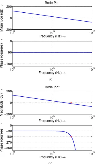
2.4 Bode plots for (a) a Type I OPLL and (b) a Type I OPLL with a
propagation delay of 10 ns. The phase-crossover frequency is indicated
by the marker in (b). . . 18
2.5 Type I, second-order OPLL using an active filter. . . 20
2.6 Variation of the minimum variance of the phase error as a function of
the normalized gain for a Type I OPLL in the presence of propagation
delay. . . 22
2.7 Variation of (a) the π-crossover frequency ¯fπ and (b) the maximum
stable loop gain ¯KL,max as a function of the position of the loop zero ¯τ0,
for a Type II OPLL in the presence of a delay τL. . . 24
2.8 Variation of the minimum variance of the phase error as a function of
the parameter ¯τ0, for a Type II OPLL with delay τL. . . 25
2.9 Experimentally measured FM response of a commercial DFB laser with
a theoretical fit using a low-pass filter model. . . 26
2.10 Bode plots for (a) a Type I OPLL including the SCL FM response, and
2.11 Practical OPLL configuration, including a lead filter to increase the
phase-crossover frequency and a low frequency active lag filter
(imple-mented by the parallel arm) to increase the hold-in range. . . 31
2.12 Phase-locking results using various commercially available SCLs. . . 34
2.13 Cartoon representation of the phase response of a single-section SCL
showing the regimes of operation of a conventional OPLL and a
sideband-locked OPLL. . . 36
2.14 Schematic diagram of a heterodyne sideband-locked OPLL. . . 37
2.15 Measured FM response of the DFB SCL used in the sideband locking
experiment. . . 39
2.16 Beat spectrum between the locked sideband of the slave SCL and the
master laser. . . 40
2.17 Lineshape measurements of the master laser, free-running and
phase-locked optical sideband of the slave SCL, using a delayed self-heterodyne
interferometer with a frequency shift of 290 MHz. . . 41
2.18 (a) Schematic diagram of the double-loop configuration. (b) Linearized
small-signal model for phase propagation. . . 43
2.19 (a) Schematic diagram of the composite heterodyne OPLL. (b)
Lin-earized small-signal model for phase propagation. . . 46
2.20 Experimentally measured frequency modulation of a single-section
dis-tributed feedback semiconductor laser and theoretical fit using equation
(2.40). . . 48
2.21 Calculated two-sided spectral densities of the residual phase error in the
loop, according to equations (2.18), (2.56) and (2.60). The variance of
the phase error is the area under the curves. . . 50
2.22 Measured spectrum of the beat signal between the optical output and
the master laser for an SCL in (a) a heterodyne OPLL, and (b) a
2.23 Measured spectrum of the beat signal between the optical output and the
master laser for an SCL in (a) a heterodyne OPLL, and (b) a composite
PLL shown in figure 2.19. . . 53
3.1 Individual SCLs all lock to a common narrow-linewidth master laser,
thus forming a coherent array. An offset RF signal is used in each loop
for additional control of the optical phase. . . 56
3.2 Measured linewidths of the master fiber laser, and the free-running and
phase-locked slave SCL. . . 58
3.3 Measured frequency noise spectra of the master fiber laser, and the
free-running and phase-locked slave DFB semiconductor laser. The green
curve is the theoretical calculation of the frequency noise spectrum of
the phase-locked slave laser using equation (3.1) and the measured loop
parameters. . . 59
3.4 Delayed self-heterodyne interferometer experiment . . . 60
3.5 Model of the power spectral density of the frequency noise of the master
laser and the free-running and locked slave laser. The OPLL is assumed
to be “ideal” with a loop bandwidth fL. . . 62
3.6 Variation of the accumulated phase error varianceσ2
∆φ(Td) vs.
interfer-ometer delay time Td for various values of the loop bandwidth fL. . . . 65
3.7 Spectral density of the optical field for different values of the loop
band-width fL, calculated using equation (3.15). . . 67
3.8 Spectral density of the detected photocurrent in a delayed self
hetero-dyne experiment using the free-running slave laser, the phase-locked
slave laser, and the master laser, for different values of the
interferome-ter delay Td. . . 71
3.9 Spectrum of the beat signal between the phase-locked slave SCL and
3.10 Measured Allan variance of the beat signal between the slave and master
lasers for the locked and unlocked cases. The variance of the RF offset
signal is also shown. . . 76
3.11 Measured Allan variance of the beat signal between the phase-locked
slave laser and the master laser, and the theoretical calculation based
on equation (3.38). . . 78
3.12 Residual phase error calculated from the measured Allan variance using
equation (3.41). . . 80
4.1 Coherent power-combining scheme using heterodyne SCL-OPLLs.
Indi-vidual SCLs all lock to a common master laser, thus forming a coherent
array. The outputs of the individual lasers are coherently combined to
obtain a high power single-mode optical beam. . . 83
4.2 (a) Coherent combination schematic. (b) Experimentally measured
com-bined power using two high power MOPAs as slave lasers phase-locked
to a common master laser. . . 85
4.3 (a) Schematic of the coherent combination experiment with additional
electronic phase control. (b) Experimentally measured combined power
using External Cavity SCLs at 1064 nm, without and with the VCO
loop connected. . . 87
4.4 Steady-state model for the loop OPLL 2 shown in figure 4.3(a). . . 89
4.5 Small-signal phase model for the power-combining scheme with the
ad-ditional VCO loop. . . 92
4.6 Binary tree configuration for the power combination of a number of SCLs
locked to a common master laser in the filled-aperture configuration. . 94
4.7 A one-dimensional array of coherent optical emitters. . . 97
4.9 Measured far-field intensities on the infrared camera for ds = 0.25 mm,
when (a) one of the OPLLs is unlocked and (b), (c) both OPLLs are
locked. The RF phase is varied between (b) and (c), demonstrating
electronic steering of the optical beam. . . 100
4.10 Horizontal far-field intensity distributions demonstrating beam-steering
of half a fringe by an RF phase shift of π radians, for emitter spacings
of (a) ds = 0.25 mm and (b) ds = 0.5 mm. The incoherently added
intensity distribution is also shown in (a). . . 101
4.11 Comparison of the experimental far-field intensity distribution with the
theoretical calculation. . . 102
4.12 Separation between fringes as a function of the inverse beam separation
d−1
s , compared to theory. . . 102
5.1 Optoelectronic feedback loop for the generation of accurate broadband
linear chirps. The optical portion of the loop is shown in blue. . . 108
5.2 Small-signal phase propagation in the optoelectronic SFL feedback loop. 111
5.3 Measured spectrograms of the output of the loop photodetector, for the
(a) free-running and (b) predistorted cases. The predistortion
signifi-cantly reduces the SCL nonlinearity. The delay of the MZI isτ = 28.6 ns.113
5.4 Measured spectrogram of the output of the loop photodetector when
the loop is in lock, showing a perfectly linear optical chirp with slope
100 GHz/ms. (b) Fourier transform of the photodetector output
mea-sured over a 1 ms duration. . . 115
5.5 Measured optical spectrum of the locked swept-frequency SCL. RBW =
10 GHz. . . 116
5.6 Experimental demonstration of generation of a perfectly linear chirp of
500 GHz / 0.1 ms using a VCSEL. (a), (b), and (c) Spectrograms of the
optical chirp slope for a ramp input, after iterative predistortion and the
5.7 Measured spectrograms of the output of the loop photodetector,
illus-trating arbitrary sweeps of the SCL frequency. (a) The reference signal is
swept linearly with time. (b) The reference signal is swept exponentially
with time. The laser sweep rate varies between 50 and 150 GHz/ms. . 119
5.8 Schematic diagram of an FMCW ranging experiment with a linearly
chirped optical source. . . 120
5.9 Range resolution measurements using the optoelectronic swept-frequency
VCSEL. . . 121
5.10 High-Qmode of a silica microtoroid in air, measured using an
optoelec-tronic SFL at 1539 nm. . . 124
5.11 Whispering gallery mode resonances of a microtoroid in water, measured
using optoelectronic SFLs at (a) 1539 nm and (b) 1310 nm. . . 125
5.12 Specific sensing of 8-isoprostane using a microtoroid resonator and an
optoelectronic SFL at 1310 nm. . . 127
6.1 (a) Schematic diagram of the four-wave mixing (FWM) experiment for
chirp bandwidth-doubling. (b) Spectral components of the input and
FWM-generated fields. The chirp-doubled component is optically
fil-tered to obtain the output waveform. . . 131
6.2 Output power as a function of the input frequency difference, for
dif-ferent values of fiber length and input power (Pch = PR = P). The
dispersion, loss and nonlinear coefficient of the fiber are described in the
text. . . 135
6.3 (a) Multisegment waveguide for quasi-phase-matching. The evolutions
of the output fieldAout(z) along the waveguide for one and two segments
are shown in (b) and (c) respectively. . . 137
6.4 Comparison of the generated FWM field in a structure with 3 segments
of lengths L each and alternating dispersions of ±Dc, with a single
6.5 Schematic diagram of the experimental setup for the demonstration of
chirp bandwidth-doubling by four-wave mixing. . . 141
6.6 Experimental demonstration of bandwidth-doubling by FWM. . . 141
6.7 Measured slopes of the (a) input and (b) output optical chirps
demon-strating the doubling of the optical chirp slope by FWM. . . 143
6.8 Improvement in the FWM power using a two-segment HNLF. . . 144
6.9 Theoretically calculated output power as a function of the input
fre-quency difference for the two-segment dispersion compensated HNLF,
compared to the same lengths (Ltot = 200 m) of individual fibers. . . . 145
6.10 Experimental demonstration of improved bandwidth using a
quasi-phase-matched nonlinear fiber. . . 145
6.11 Comparison of the normalized experimentally measured FWM power
in two individual segments of 100 m each with opposite signs of the
dispersion parameter, and the dispersion-compensated two-segment fiber.147
6.12 Cascaded FWM stages for geometric scaling of the chirp bandwidth.
Each stage consists of a coupler, amplifier, HNLF and filter as shown in
figure 6.1(a). . . 148
6.13 Spectral components in a bandwidth tripling FWM experiment using
two chirped optical inputs. . . 149
6.14 (a) FWM “engine” for geometric scaling of the chirp bandwidth. The
filter is switched every T seconds so that it passes only the FWM
com-ponent generated. (b) Output frequency vs. time. . . 150
6.15 (a) Schematic diagram of an FMCW ranging experiment with a linearly
chirped optical source. (b) Variation of the optical frequency with time. 152
6.16 Illustration of the MS-FMCW concept. . . 156
6.17 Schematic of a multiple source FMCW ranging experiment. A reference
target is imaged along with the target of interest, so that the intersweep
gaps may be recovered. . . 157
6.18 Architecture of a potential MS-FMCW imaging system. . . 159
6.20 Experimental MS-FMCW results using a VCSEL. . . 162
7.1 Schematic diagram of a potential compact integrated label-free
biomolec-ular sensor. . . 166
A.1 Variation of (a) the normalized π-crossover frequency and (b) the
nor-malized maximum gain as a function of the parameter b in equation
(A.1). . . 169
A.2 Variation of the integralI(b,K¯F) in equation (A.6) as a function of ¯KF,
for b= 1.64. . . 170
A.3 Variation of the (a) normalized optimum gain ¯KF,opt = KF,opt/fc and
(b) the normalized minimum residual phase error σ2
minfc/(∆νm+ ∆νs)
as a function of the parameterb, for a first-order OPLL with a SCL with
nonuniform FM response. . . 171
List of Tables
1.1 Comparison between electronic PLLs and OPLLs . . . 3
2.1 Parameters of OPLLs demonstrated using commercially available SCLs 32
2.2 Parameters and results of the numerical calculations of the performance
of composite OPLLs . . . 50
6.1 Length of HNLF and input power requirements for different output
Glossary of Acronyms
CBC Coherent beam-combining
CCO Current-controlled oscillator
DFB Distributed feedback
EDFA Erbium-doped fiber amplifier
FM Frequency modulation
FMCW Frequency modulated continuous wave
FWHM Full width at half maximum
FWM Four-wave mixing
GVD Group velocity dispersion
HNLF Highly nonlinear fiber
LIDAR Light detection and ranging
MOPA Master oscillator power amplifier
MS-FMCW Multiple source-frequency modulated continuous wave
MZI Mach-Zehnder interferometer
OCT Optical coherence tomography
PD Photodetector
PLL Phase-locked loop
RIN Relative intensity noise
RF Radio frequency
SCL Semiconductor laser
SFL Swept-frequency laser
SS-OCT Swept source-optical coherence tomography
VCO Voltage-controlled oscillator
VCSEL Vertical cavity surface-emitting laser
Chapter 1
Overview
1.1
Introduction
The modulation of the intensity of optical waves has been extensively studied over
the past few decades and forms the basis of almost all of the information applications
of lasers to date. This is in contrast to the field of radio frequency (RF) electronics
where the phase of the carrier wave plays a key role. Specifically, phase-locked loop
(PLL) systems [1, 2] are the main enablers of many applications such as wireless
communications, clock delivery, and clock recovery, and find use in most modern
electronic appliances including cellphones, televisions, pagers, radios, etc.
The semiconductor laser (SCL) is the basic building block of most optical
com-munication networks, and has a number of unique properties, such as its very large
current-frequency sensitivity, fast response, small volume, very low cost, robustness,
and compatibility with electronic circuits. This work focuses on utilizing these unique
properties of an SCL not only to import to optics and optical communication many
of the important applications of the RF field, but also to harness the wide
band-width inherent to optical waves to enable a new generation of photonic and RF
systems. We demonstrate novel uses of optoelectronic phase and frequency control
in the fields of sensor networks, high power electronically steerable optical beams,
ar-bitrary waveform synthesis, and wideband precisely controlled swept-frequency laser
sources for three-dimensional imaging, chemical sensing and spectroscopy. Phase
Figure 1.1. Schematic diagram of a generic phase-locked loop.
two optoelectronic feedback systems: the optical phase-locked loop (OPLL) and the
optoelectronic swept-frequency laser (SFL).
1.2
Optical Phase-Locked Loops (OPLLs) and
Ap-plications
A PLL is a negative-feedback control system where the phase and frequency of a
“slave” oscillator is made to track that of a reference or “master” oscillator. As
shown in figure 1.1, a generic PLL has two important parts: a voltage-controlled
oscillator (VCO), and a phase detector that compares the phases of the slave and
master oscillators. The optical analogs of these electronic components are listed in
table 1.1. A photodetector acts as a mixer since the photocurrent is proportional to
the intensity of the incident optical signal; two optical fields incident on the detector
result in a current that includes a term proportional to the product of the two fields.
The SCL is a current-controlled oscillator (CCO) whose frequency is controlled via
its injection current, thereby acting as the optical analog of an electronic VCO.
Ever since the first demonstration of a laser PLL [3] only five years after the first
demonstration of the laser [4], OPLLs using a variety of lasers oscillators have been
investigated by various researchers [5–24]. One of the basic requirements of an OPLL
Table 1.1. Comparison between electronic PLLs and OPLLs
Electronic PLL Optical PLL (OPLL)
Master oscillator Electronic oscillator High-quality laser
Slave oscillator Voltage-controlled oscillator Semiconductor laser
(current-controlled oscillator)
Phase detector Electronic mixer Photodetector
the loop bandwidth, as shown in chapter 2. SCLs tend to have large linewidths (in
the megahertz range) due to their small size and the linewidth broadening effect due
to phase-amplitude coupling [25–28]. Therefore, OPLL demonstrations have typically
been performed using specialized lasers such as solid-state lasers [5–9], gas lasers [10],
external cavity lasers [11–16] or specialized multisection SCLs [17–23] which have
narrow linewdths and desirable modulation properties. In this work, we explore
OPLLs based on different commercially available SCLs, taking advantage of recent
advances in laser fabrication that have led to the development of narrow-linewidth
distributed feedback (DFB) and other types of SCLs. Further, we develop new
phase-locking architectures that eliminate the need for specialized SCL design and enable
the phase-locking of standard single-section DFB SCLs.
Research into OPLLs was mainly driven by interest in robust coherent optical
communication links for long-distance communications in the 1980s and early 1990s,
but the advent of the erbium doped fiber amplifier (EDFA) [29, 30] and difficulties in
OPLL implementation made coherent modulation formats unattractive. Interest in
OPLL research has been renewed recently, for specialized applications such as
free-space and intersatellite optical communication links, extremely high bandwidth
opti-cal communication, clock distribution etc. It is no surprise, then, that the majority of
OPLL research has focused on applications in phase-modulated coherent optical
com-munication links [5, 6, 17, 18, 31–36], clock generation and transmission [14, 19, 37–39],
synchronization and recovery [21,40]. More recent work has investigated applications
≈
O
p
ti
c
a
l
F
re
q
u
e
n
cy
ω
L
Time
ξτ
τ
2
π
B
ω
0+
ξ
t
Laun ched
Ref lect
ed
Figure 1.2. A frequency-modulated continuous wave (FMCW) experiment.
and phase-sensitive amplification [15, 44], to name a few.
In this work, we instead look at novel applications that focus on arrays of
phase-locked lasers that form phase-controlled apertures with electronic control over the
shape of the optical wavefront. We first show that the coherence properties of the
master laser are “cloned” onto the slave laser, by direct measurements of the phase
noise of the lasers in the frequency and time domains. This coherence cloning
en-ables an array of lasers which effectively behaves as one coherent aperture, but with
electronic control over the individual phases. We study applications of these
phase-controlled apertures in coherent power-combining and electronic beam-steering.
1.3
Optoelectronic Swept-Frequency Lasers (SFLs)
Swept-frequency lasers have an important application in the field of three-dimensional
(3-D) imaging, since axial distance can be encoded onto the frequency of the optical
waveform. In particular, consider an imaging experiment with an SFL source whose
frequency varies linearly with time, with a known slope ξ, as shown in figure 1.2.
When the reflected signal with a total time delay τ is mixed with the SFL output, a
beat term with frequency ξτ is generated, and the time delayτ can by calculated by
measuring the frequency of the beat note. This is the principle of frequency modulated
continuous wave (FMCW) reflectometry, also known as optical frequency domain
does not require high-speed electronics [45], FMCW reflectometry finds applications
in light detection and ranging (LIDAR) [46–49] and in biomedical imaging [50, 51],
where the experiment described above is known, for historical reasons, as swept source
optical coherence tomography (SS-OCT). In fact, SS-OCT is now the preferred form
of biomedical imaging using OCT, and represents the biggest potential application for
SFL sources. Other applications include noncontact profilometry [52], biometrics [53],
sensing and spectroscopy. The key metrics for an SFL are the total chirp (or “chirp
bandwidth”) B—the axial range resolution of the SFL is inversely proportional to
B [54, 55]—and the chirp speed ξ, which determines the rate of image acquisition. It
is desirable for the SFL to sweep rapidly across a very large bandwidth B.
State-of-the-art SFL sources for biomedical and other imaging applications are
typically mechanically tuned external cavity lasers where a rotating grating tunes
the lasing frequency [50, 56, 57]. Fourier-domain mode locking [58] and quasi-phase
continuous tuning [59] have been developed to further improve the tuning speed and
lasing properties of these sources. However, all these approaches suffer from complex
mechanical embodiments that limit their speed, linearity, coherence, reliability and
ease of use and manufacture. In this work, we develop a solid-state optoelectronic SFL
source based on an SCL in a feedback loop. The starting frequency and slope of the
optical chirp are locked to, and determined solely by, an electronic reference oscillator.
By tuning this oscillator, we demonstrate the generation of arbitrary optical
wave-forms. The use of this precisely controlled optoelectronic SFL in a high-sensitivity
label-free biomolecular sensing experiment is demonstrated.
While single-mode SCLs enable optoelectronic control and eliminate the need
for mechanical tuning elements, they suffer from a serious drawback: their tuning
range is limited to <1 THz. High resolution biomedical imaging applications require
bandwidths of ≥10 THz to resolve features tens of microns in size. We therefore
develop and demonstrate two techniques to increase the chirp bandwidth of SFLs,
namely four-wave mixing (FWM) and algorithmic “stitching” or multiple
source-(MS-) FMCW reflectometry. When the chirped output from an SFL is mixed with a
the optical chirp is generated by the process of FWM. We show that this wave
re-tains the chirp characteristics of the original chirped wave, and is therefore useful for
imaging and sensing applications. As do all nonlinear distributed optical interactions,
the efficiency of the above scheme suffers from lack of phase-matching. We develop a
quasi-phase-matching technique to overcome this limitation. On the other hand, the
MS-FMCW technique helps to generate high resolution images using distinct
mea-surements taken using lasers that sweep over different regions of the optical spectrum,
in an experiment similar to synthetic aperture radio imaging [60].
1.4
Organization of the Thesis
This thesis is organized as follows. SCL-OPLLs are described in chapter 2, including
theoretical analyses and experimental characterizations. The limitations imposed by
the FM response of a single-section SCL are described, and two techniques developed
to overcome these limitations are described, viz. sideband locking [61] and composite
OPLLs [62].
OPLL applications are described in chapters 3 and 4. The cloning of the coherence
of the master laser in an OPLL onto the slave SCL [63] is thoroughly characterized,
theoretically and experimentally, in chapter 3. Frequency domain (spectrum of the
laser frequency noise) and time domain (Allan variance) measurements are performed
and are shown to match theoretical predictions. The effect of coherence cloning on
interferometric sensing experiments is analyzed. Applications of arrays of
phase-locked SCLs are studied in chapter 4. These include coherent power-combining [64–67]
and electronic beam-steering [68].
The optoelectronic SFL developed in this work [69] is described in chapter 5,
and the generation of precisely controlled arbitrary swept-frequency waveforms is
demonstrated. An application of the SFL to biomolecular sensing is studied. The
extension of the bandwidth of swept-frequency waveforms for high resolution imaging
applications is the focus of chapter 6. Two methods to achieve this: FWM [70] and
A summary of the work and a number of possible directions to further develop
Chapter 2
Semiconductor Laser Optical
Phase-Locked Loops
2.1
OPLL Basics
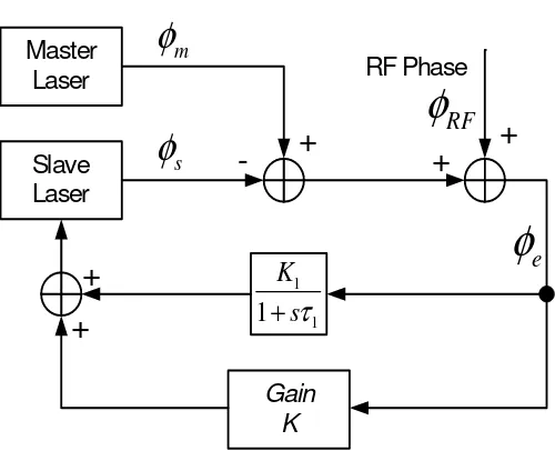
The SCL-OPLL, shown in figure 2.1, is a feedback system that enables electronic
control of the phase of the output of an SCL. The fields of the master laser and the
slave SCL are mixed in a photodetector PD. A part of the detected photocurrent is
monitored using an electronic spectrum analyzer. The detected output is amplified,
mixed down with an “offset” radio frequency (RF) signal, filtered and fed back to the
SCL to complete the loop.
A schematic model of the OPLL is shown in figure 2.2(a). We will assume that the
free-running SCL has an outputascos ωf rs t+φf rs (t)
, where the “phase noise”φf r
s (t)
is assumed to have zero mean. When the loop is in lock, we drop the superscript f r
from the laser phase and frequency variables. Similarly, the master laser output is
given by amcos (ωmt+φm(t)). The detected photocurrent is then
iP D(t) =ρ a2m+a2s+ 2asamcos [(ωm−ωs)t+ (φm(t)−φs(t))]
, (2.1)
where ρ is the responsivity of the PD. The last term above shows that the PD
acts as a frequency mixer in the OPLL. Let us further define a photodetector gain
KP D = 2. ρhasami, where h.i denotes the average value. The detected photocurrent
00000000000000000000000000000000000000000000000000000000000000000000000000000000000000000000000000000000000000000000000000000000 00000000000000000000000000000000000000000000000000000000000000000000000000000000000000000000000000000000000000000000000000000000 00000000000000000000000000000000000000000000000000000000000000000000000000000000000000000000000000000000000000000000000000000000 00000000000000000000000000000000000000000000000000000000000000000000000000000000000000000000000000000000000000000000000000000000 00000000000000000000000000000000000000000000000000000000000000000000000000000000000000000000000000000000000000000000000000000000 00000000000000000000000000000000000000000000000000000000000000000000000000000000000000000000000000000000000000000000000000000000 00000000000000000000000000000000000000000000000000000000000000000000000000000000000000000000000000000000000000000000000000000000 00000000000000000000000000000000000000000000000000000000000000000000000000000000000000000000000000000000000000000000000000000000 00000000000000000000000000000000000000000000000000000000000000000000000000000000000000000000000000000000000000000000000000000000 00000000000000000000000000000000000000000000000000000000000000000000000000000000000000000000000000000000000000000000000000000000 00000000000000000000000000000000000000000000000000000000000000000000000000000000000000000000000000000000000000000000000000000000 00000000000000000000000000000000000000000000000000000000000000000000000000000000000000000000000000000000000000000000000000000000
Semiconductor
Laser
0000000000000000000000000000000000000000000000000000000000 0000000000000000000000000000000000000000000000000000000000 0000000000000000000000000000000000000000000000000000000000 0000000000000000000000000000000000000000000000000000000000 0000000000000000000000000000000000000000000000000000000000 0000000000000000000000000000000000000000000000000000000000PD
Gain
0000000000000000000000000000000000000000000000000000000000 0000000000000000000000000000000000000000000000000000000000 0000000000000000000000000000000000000000000000000000000000 0000000000000000000000000000000000000000000000000000000000 0000000000000000000000000000000000000000000000000000000000 0000000000000000000000000000000000000000000000000000000000Filter
00000000000000000000000000000000000000000000000000000000000000000000000000000000000000 00000000000000000000000000000000000000000000000000000000000000000000000000000000000000 00000000000000000000000000000000000000000000000000000000000000000000000000000000000000 00000000000000000000000000000000000000000000000000000000000000000000000000000000000000 00000000000000000000000000000000000000000000000000000000000000000000000000000000000000 00000000000000000000000000000000000000000000000000000000000000000000000000000000000000 00000000000000000000000000000000000000000000000000000000000000000000000000000000000000 00000000000000000000000000000000000000000000000000000000000000000000000000000000000000RF Offset
00000000000000000000000000000000000000000000000000000000000000000000000000000000000000000000000000000000000000000000000000000000 00000000000000000000000000000000000000000000000000000000000000000000000000000000000000000000000000000000000000000000000000000000 00000000000000000000000000000000000000000000000000000000000000000000000000000000000000000000000000000000000000000000000000000000 00000000000000000000000000000000000000000000000000000000000000000000000000000000000000000000000000000000000000000000000000000000 00000000000000000000000000000000000000000000000000000000000000000000000000000000000000000000000000000000000000000000000000000000 00000000000000000000000000000000000000000000000000000000000000000000000000000000000000000000000000000000000000000000000000000000 00000000000000000000000000000000000000000000000000000000000000000000000000000000000000000000000000000000000000000000000000000000 00000000000000000000000000000000000000000000000000000000000000000000000000000000000000000000000000000000000000000000000000000000 00000000000000000000000000000000000000000000000000000000000000000000000000000000000000000000000000000000000000000000000000000000 00000000000000000000000000000000000000000000000000000000000000000000000000000000000000000000000000000000000000000000000000000000 00000000000000000000000000000000000000000000000000000000000000000000000000000000000000000000000000000000000000000000000000000000Master Laser
(Fiber Laser)
0000000000000000000000000000000000000000000000000000000000000000000000000000000000000000000000000000000000000000000000000 0000000000000000000000000000000000000000000000000000000000000000000000000000000000000000000000000000000000000000000000000 0000000000000000000000000000000000000000000000000000000000000000000000000000000000000000000000000000000000000000000000000 0000000000000000000000000000000000000000000000000000000000000000000000000000000000000000000000000000000000000000000000000 0000000000000000000000000000000000000000000000000000000000000000000000000000000000000000000000000000000000000000000000000 0000000000000000000000000000000000000000000000000000000000000000000000000000000000000000000000000000000000000000000000000 0000000000000000000000000000000000000000000000000000000000000000000000000000000000000000000000000000000000000000000000000 0000000000000000000000000000000000000000000000000000000000000000000000000000000000000000000000000000000000000000000000000 0000000000000000000000000000000000000000000000000000000000000000000000000000000000000000000000000000000000000000000000000Spectrum
Analyzer
Figure 2.1. A heterodyne semiconductor laser optical phase-locked loop. PD: photo-detector.
be aRFsin (ωRFt+φRF(t)). The choice of trigonometric functions ensures a mixer
output of the form
iM(t) =±KMKP DaRFsin [(ωm−ωs±ωRF)t+ (φm(t)−φs(t)±φRF(t))]. (2.2)
Without loss of generality, we will consider only the “+” sign in the rest of this thesis.
This mixer output is amplified with gain Kamp, filtered and fed into the SCL, which
acts as a current-controlled oscillator whose frequency shift is proportional to the
input current, i.e.,
δωs=−Ksis(t) =−KsKampiM(t) (2.3)
The minus sign indicates that the frequency of the SCL decreases with increasing
current. A propagation delayτL is included in the analysis. We will assume that the
filter has a unity gain at DC, i.e., the area under its impulse response is zero. We
lump together the DC gains of the various elements in the loop, and denote it byKdc,
i.e., Kdc = aRFKMKP DKampKs. This parameter will shortly be defined in a more
rigorous manner. When in lock, the frequency shift of the SCL is given by
Loop Filter Master Laser
Laser Phase-Locked to Master
Local
Oscillator (LO) SCL
ωst+φs
ωmt+φm
Phase Error
ωRFt+φRF RF Offset
φe
Mixer Photodetector
τL Delay
Gain
Kdc (a)
φf r
s (s)
PD
Ff(s)
φs(s)
Gain Kdccos (φe0)
Kdcsin (φe0)r(s)/2
Delay
Filter SCL
e
−sτLFF M(s)×1/s
φm(s) +φRF(s)
(b)
Figure 2.2. (a) Schematic diagram of an OPLL. (b) Linearized small-signal model for phase noise propagation in the OPLL.
The frequency of the slave laser is the sum of the free-running frequency and the
correction from the feedback loop, i.e.,
ωs =ωsf r+δωs. (2.5)
The free-running frequency difference between the slave and master lasers (offset
by the RF frequency) is defined as
∆ωf r =. ωm−ωsf r+ωRF. (2.6)
We now derive the the steady-state operating point of this laser [2]. In steady state,
time, which yields
ωs = ωm+ωRF,
¯
φs = ¯φm+ ¯φRF +φe0.
(2.7)
The bars in the second part of equation (2.7) denote that this equation is valid for the
steady-state values of the phase. The parameterφe0 is the steady-state phase error in
the loop. This phase error is a consequence of the feedback current keeping the loop
in lock, which can be understood by substituting equation (2.7) into equation (2.4)
and using equations (2.5) and (2.6) to obtain
δωs = ∆ωf r =Kdcsinφe0. (2.8)
The frequency shift induced by the feedback loop, δωs, compensates for the
free-running frequency difference between the slave and master lasers, and its maximum
value is limited by the DC gain of the loop. The maximum value of the free-running
frequency difference that the loop can tolerate in lock is called the “hold-in range,”
and is defined in section 2.1.2. The steady-state phase error is given by
φe0 = sin−1
∆ωf r
Kdc
. (2.9)
It is important that the DC gainKdcbe as large as possible and the laser free-running
frequency fluctuations be minimized, so that φe0 is small. Indeed, this is the case in
most well-designed OPLLs, and we will ignore this steady state phase error in large
parts of this thesis. In the absence of φe0, the phase of the locked slave SCL exactly
follows that of the master laser, offset by the RF phase.
The heterodyne OPLL of figure 2.1 differs from the homodyne PLL shown in
figure 1.1 in the addition of an extra reference (“offset”) RF oscillator. This results
in some powerful advantages: as is clear from equation (2.7), the optical phase can be
controlled in a degree for degree manner by adjusting the electronic phase of the offset
signal. Further, heterodyne locking ensures that the beat note at the photodetector
and can easily be separated from the low frequency (“DC”) terms.
2.1.1
Small-Signal Analysis
The OPLL is next linearized about the steady-state operating point given in equation
(2.7) and the propagation of the phase around the loop is analyzed in the Laplace
domain [2], as shown in figure 2.2(b). The variables in the loop are the Laplace
transforms of the phases of the lasers and the RF signal.1 Fourier transforms are also
useful to understand some loop properties, and will be used in parts of the thesis. The
Fourier transformX(f) is the Laplace transformX(s) evaluated along the imaginary
axis, s = j2πf. The notation X(ω) is also used in literature to denote the Fourier
transform, with the angular Fourier frequency, ω, given byω = 2πf; we will useX(f)
in this thesis to avoid confusion. It is to be understood that the steady-state values
of the phase in equation (2.7) are subtracted from the phases before the Laplace
(or Fourier) transform is computed. The free-running phase fluctuation of the slave
SCL (“phase noise”) is denoted by the additive term φf r
s (s).2 The summed relative
intensity noises of the lasers r(s) are also incorporated into the model.3
The SCL acts as a current-controlled oscillator and, in the ideal case, produces
an output phase equal to the integral of the input current for all modulation
fre-quencies, i.e. it has a transfer function 1/s. However, the response of a practical
SCL is not ideal, and the change in output optical frequency is a function of the
frequency components of the input current modulation. This dependence is modeled
by a frequency-dependent FM response FF M(s). The shape of the FM response and
1
Notation: the Laplace transform of the variablex(t) is denoted byX(s). For Greek letters, the Fourier transform ofφ(t) is just denoted byφ(s). The argumentsis sometimes dropped when the usage is clear from the context.
2
Strictly speaking, the Laplace or Fourier transform of the phase noise cannot be defined—it is a random process, and we can only describe its spectral density. However, the use of Laplace transforms provides valuable insight—for this purpose, we can regard the observed phase noise as a particular instance of the underlying random process. The spectral density will be used in all calculations involving the phase noise, e.g., see chapter 3.
3
The model of figure 2.2(b) is easily derived by noting that the expansion of the phase detec-tor output Kdc(1 +r(t)/2) sin (φe0+φe(t)) about the steady state value Kdcsinφe0 isKdcsinφe0 + (Kdcsinφe0)r(t)/2 + (Kdccosφe0)φe(t). The relative amplitude noise is one-half the relative
its effects are discussed in section 2.3. The filter response and the FM response of
the SCL are assumed to be normalized to have unit gain at DC, i.e., Ff(0) = 1,4
FF M(0) = 1. For simplicity, we have also assumed that the photodetector and mixer
have flat frequency responses—this is true if wideband detectors and mixers are used
in the loop, as is the case in this work. It is straightforward to include nonuniform
detector and mixer responses in the analysis.
Let us define the open-loop transfer function of the loop as the product of the
transfer functions of all the elements in the loop for the ideal caseφe0 = 0:
Gop(s) =
KdcFf(s)FF M(s)e−sτL
s . (2.10)
This allows us to define the DC gain in a more rigorous manner:
Kdc = lim.
s→0sGop(s). (2.11)
The phase of the locked SCL is then given by
φs(s) = (φm(s) +φRF(s))
Gopcosφe0
1 +Gopcosφe0
+ φ
f r s (s)
1 +Gopcosφe0
+r(s)
2
Gopsinφe0
1 +Gopcosφe0
,
(2.12)
where we have omitted the argument s in Gop(s). Phase noise, φf rs (s), represents
the largest source of noise in an SCL-OPLL due to the relatively large linewidth of
an SCL, and the contribution of the last term on the right-hand side can usually be
neglected, especially if φe0 ≈ 0. We will therefore ignore the laser relative intensity
noise in the rest of this thesis. For similar reasons, we also neglect the effects of
shot noise and detector noise on the phase of the SCL in this thesis. It will also be
assumed, unless stated otherwise, that φe0 = 0.
4
2.1.2
OPLL Performance Metrics
We now define the important OPLL performance metrics that will be used in this
work.
Loop bandwidth is the largest Fourier frequency for which the open loop transfer
functionGop(f) is larger than unity. From equation (2.12), this means thatthe
phase of the locked SCL follows that of the master and the RF offset within the
loop bandwidth, and reverts to the free-running value at higher frequencies. The
loop bandwidth is usually limited by the stability of the loop—in particular,
we will use the Bode stability criterion [2], which states that the magnitude
of the complex valued function Gop(f) should be lesser than unity when its
phase is lesser than or equal to−π. The frequency at which the phase response
equals −π is referred to as the “phase-crossover frequency” and represents the
maximum possible value of the loop bandwidth.
Hold-in range is defined as the largest change in the free-running frequency of the
slave SCL over which the loop still remains in lock. This can be evaluated from
equation (2.8), where the sine function takes a maximum value of unity. Using
equation (2.11), we write the hold-in range as
fhold =
1
2πslim→0sGop(s). (2.13)
Clearly, a large hold-in range is desired so that the loop is insensitive to
envi-ronmental fluctuations.
Residual phase error in the loop is one of the most important metrics to evaluate
the performance of the loop. It is defined as the variance in the deviation of the
phase of the locked SCL from the ideal case where it follows the master laser,
i.e.,
σφ2 =
(φs(t)−φm(t)−φRF(t))2
where h.i denotes averaging over all time.5 Using the Wiener-Khintchine
theo-rem, equation (2.14) can be written in the frequency domain as
σφ2 =
Z ∞
−∞
Sφe(f)df, (2.15)
whereSe
φ(f) is the spectral density of the random variableφs(t)−φm(t)−φRF(t),
i.e., the spectrum of the phase error. Using equation (2.12), and assuming
φe0 = 0, we have
Sφe(f) =
1
1 +Gop(f)
2
Sφm(f) +Sφs,f r(f), (2.16)
where we have used the fact that the phase noise of the master laser and
free-running slave laser are uncorrelated. Sm
φ(f) and S
s,f r
φ (f) are the spectra of the
phase noise of the master and free-running slave SCL respectively, and the phase
noise of the RF source is assumed to be negligible. Under the assumption of a
Lorenzian lineshape for the lasers, these spectral densities are related to their
3 dB linewidths ∆ν by [72]
Sm
φ(f) =
∆νm
2πf2,
Sφs,f r(f) = ∆νs
2πf2.
(2.17)
Using (2.16) and (2.17) in (2.15), we obtain the result for the variance of the
residual phase error of the OPLL:
σφ2 = ∆νm + ∆νs
2π Z ∞ −∞ 1 f2 1
1 +Gop(f)
2 df. (2.18)
For a stable OPLL, we require that σ2
φ≪ 1 rad2. σφ is the standard deviation
of the residual phase error, measured in radians.
Settling time is defined as the time taken by the error signal in the loop to relax
back to its steady-state value, within 1%, when a step phase input ∆φis applied.
5
Open-loop transfer function
Gop(f)
φm(f)
φs(f)
PD
φf r s (f)
Figure 2.3. Simplified schematic diagram of an OPLL.
If the step is applied at t = 0, the phase error goes from (φe0+ ∆φ) to (φe0+
0.01∆φ) at time t=τs. Alternatively, this is the time taken by the laser phase
to change by 0.99∆φ. The settling time is of interest in applications where the
laser phase is changed using an RF phase input.
The response of the loop error signal to a step input is given by
φe(t)−φe0 =L−1
∆φ 1
s(1 +Gop(s))
, (2.19)
where L−1 is the inverse Laplace transform operator.
Other OPLL metrics such as acquisition range, mean time between cycle-slips etc.
are not central to this work and will not be considered here. Some of these metrics
are discussed in references [2, 73].
2.2
Performance of Different OPLL Architectures
We now evaluate the performance metrics listed above for three different OPLL
ar-chitectures that are relevant to this work. In this section, we assume that the FM
response of the SCL is flat, i.e., FF M(f) = 1. The “type” of an OPLL is the number
of poles6 at s = 0, and its “order” is the total number of poles. The RF source is
assumed to have no noise, which allows the OPLL to be simplified as in figure 2.3.
6
As a concrete example, let us assume that the summed linewidth of the master and
slave lasers is 0.5 MHz, which is representative of (good) DFB SCLs.
2.2.1
Type I OPLL
This OPLL has a transfer function
Gop(f) = K
j2πf, (2.20)
where the pole at f = 0 denotes that the optical phase at the output of the SCL is
obtained by integrating the input control signal. The magnitude and phase of Gop(f)
are plotted in a “Bode plot” in figure 2.4(a). Since the phase of Gop(f) never goes to
−π, this OPLL is unconditionally stable, with bandwidth and hold-in range K/2π.
Practical OPLLs are always bandwidth-limited; let us therefore arbitrarily assume
that the bandwidth of this loop is 2 MHz, i.e., K = 1.26×10⁷ rad/s.
The laser frequency drifts due to fluctuations in the laser bias current and
tem-perature. Assuming that a low noise current source is used to bias the laser, the
primary source of free-running frequency variations is environmental temperature
fluctuations. The thermal frequency tuning coefficient of InP-based lasers is typically
10 GHz/◦C. A hold-in range of 2 MHz therefore means that the loop loses lock if the
SCL temperature fluctuates by only ∼2×10⁻⁴ ◦C.
The residual phase error of this loop is given by
σφ2 = π(∆νm+ ∆νs)
K , (2.21)
which, with the assumed values of laser linewidth and loop bandwidth, yields σ2
φ =
0.4 rad2. Equation (2.21) leads us to an important general result: it is necessary that
the summed linewidths of the two lasers be much smaller than the loop bandwidth for
100 105 1010 −200
0 200
Frequency (Hz) →
Magnitude (dB)
→
Bode Plot
100 105 1010
−180 −90 0
Frequency (Hz) →
Phase (degrees)
→
(a)
100 105 1010
−200 0 200
Frequency (Hz) →
Magnitude (dB)
→
Bode Plot
100 105 1010
−360 −270 −180 −90 0
Frequency (Hz) →
Phase (degrees)
→
(b)
The response of the phase error to a step response is
φe(t)−φe0 = ∆φexp(−Kt), (2.22)
which gives a 99% settling time ofτs ≃4.6/K ≃4×10⁻⁷ s.
The high sensitivity of this loop to temperature fluctuations is due to the arbitrary
bandwidth limit assumed; however other factors such as the SCL FM response and
loop propagation delay, discussed later, do impose such a restriction. It is therefore
important to design loop filters to increase the DC gain and loop bandwidth.
2.2.2
Type I, Second-Order OPLL
The extremely high sensitivity of the basic Type I OPLL to temperature fluctuations
can be overcome using a filter Ff(f) = (1 +j2πf τ0)/(1 +j2πf τ1), with τ0 < τ1.
This filter is called a lag filter or lag compensator [74]7 since its response has a phase
lag (phase response is <0). The value of τ0 is chosen so that τ0−1 is much smaller
than the loop bandwidth, which ensures that the filter response does not affect the
phase-crossover frequency. To maintain the same value of the loop bandwidth as the
Type I OPLL, the loop gain has to be increased by a factor τ1/τ0, so that the loop
transfer function is
Gop(f) = K j2πf ×
τ1 τ0 ×
1 +j2πf τ0
1 +j2πf τ1. (2.23)
In the limit of τ1 → ∞, this loop is a Type-II control system.
The bandwidth of this loop isK/2π = 2 MHz, while the hold-in range isKτ1/2πτ0.
By proper choice ofτ1 andτ0, a hold-in range of several gigahertz can be achieved. A
hold-in range of 1 GHz corresponds to a temperature change of 0.1 ◦C, and the SCL
temperature is easily controlled to much smaller than this value.
The addition of the lag filter at low frequencies does not affect the residual phase
error σ2
φ, since most of the contribution to the integral in equation (2.18) is from
frequencies of the order of the loop bandwidth.
7
Master Laser
Slave Laser
Gain K
s
φ
mφ
e
φ
RFφ
RF Phase
+
-
+
+
1
1
1
K
s
τ
+
+
+
Figure 2.5. Type I, second-order OPLL using an active filter.
When a step input ∆φ is applied, the phase error in the loop varies as
φe(t)−φe0 =L−1 ∆φ
s+ 1/τ1 s2 +s(1
τ1 +K) + K τ0
!
. (2.24)
Using the approximation τ0−1 ≪ τ1−1 ≪ K, this is an overdamped system, and the
final solution for the phase error transient is
φe(t)−φe0 = ∆φexp(−Kt), (2.25)
which is identical to the simple Type I OPLL. The settling time of the loop is therefore
unaffected, and the OPLL settles to (99% of) the new set-point in a timeτs ≃4.6/K =
4×10⁻⁷ s.
The loop filter described above is easily realized using passive R-C circuits [66].
The drawback of a passive filter is that additional gain has to be provided by the
amplifier in the loop, which is not always feasible due to amplifier saturation. This
can be overcome using an active low-pass filter in a parallel arm [66] as shown in figure
2.5. The additional branch has high DC gain (K1 ≫K), and the pole is located at
transfer function of this loop is
Gop(f) =
1
j2πf
K+ K1
1 +j2πf τ1
, (2.26)
which is identical to equation (2.23) with τ0/τ1 =K/K1.
2.2.3
Type I OPLL with Delay
We now study an OPLL in the presence of propagation delay. It must be
empha-sized that all negative feedback systems suffer from delay limitations, but the wide
linewidth of SCLs makes the delay a very important factor in OPLLs, and has been
studied by different authors [75, 76]. The transfer function of a delay element is given
by exp(−j2πf τL) whereτLis the delay time. We write the open loop transfer function
of a first-order loop with delay τL as
G(f) = KL
jf exp(−j2πf τL)
= K¯L
jf¯ exp −j2πf¯
, (2.27)
where the normalized variables are defined as
¯
f =. f τL,
¯
KL=. KLτL. (2.28)
We identify theπ-crossover frequency and the maximum stable gain by∠G(fπ) =
−π and |G(fπ)|= 1:
¯
fπ = 1/4,
¯
KL,max = 1/4. (2.29)
The loop bandwidth is therefore limited to 1/(4τL), which is equal to the maximum
0 0.05 0.1 0.15 0.2 0.25 0
50 100 150
Normalised Loop gain K
LτL→ σ φ
2 / (
∆
ν m
+
∆
ν s
)
τ L
(rad
2 )
→
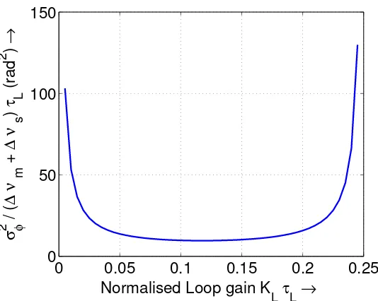
Figure 2.6. Variation of the minimum variance of the phase error as a function of the normalized gain for a Type I OPLL in the presence of propagation delay.
in figure 2.4(b), assuming a delay τL = 10 ns, which is a typical value for optical
fiber-based OPLLs. The phase crossover frequency is then equal to 25 MHz.
The variance of the residual phase error is calculated using equation (2.27) in
equation (2.18) to obtain
σ2φ=τL
∆νm+ ∆νs
2π
Z ∞
−∞
df¯
¯
K2
L+ ¯f2−2 ¯KLf¯sin(2πf¯)
. (2.30)
The calculated value of the variance of the phase error as a function of the
nor-malized gain is shown in figure 2.6. As expected, the phase error is very large at ¯
KL = 0 (no PLL correction) and ¯KL= 1/4 (borderline instability). The phase error
is minimum when ¯KL= ¯KL,opt = 0.118, and the minimum value is given by
σφ,min2 = 9.62 τL(∆νm+ ∆νs). (2.31)
2.2.4
Type II Loop with Delay
The limited hold-in range of the Type I loop of the previous loop can be improved
using a lag filter design similar to section 2.2.2. Here, we consider the limiting case
(τ1 → ∞) of a Type II OPLL. In the presence of a propagation delay τL, the open
loop transfer function is given by
G(f) = −KL(1 +j2πf τ0)
f2 exp(−j2πf τL)
=−K¯L(1 +¯j2πf¯τ0¯)
f2 exp −j2πf¯
, (2.32)
where the normalized variables are defined as
¯
f =. f τL,
¯
KL=. KLτL2,
¯
τ0 =. τ0/τL. (2.33)
The π-crossover frequency is identified by setting ∠G(fπ) =−π, to obtain
tan(2πf¯π) = 2πf¯πτ0.¯ (2.34)
A solution to this equation exists only if ¯τ0 >1, orτ0 > τL. In other words, the loop
is stable only if, at low frequencies, the phase lead introduced by the zero is larger
than the phase lag introduced by the delay. The maximum stable loop gain is given
by
¯
KL,max =
¯
f2 π
p
1 + (2πf¯πτ0¯)2
. (2.35)
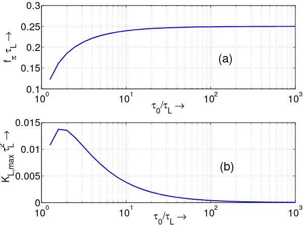
The variation of ¯fπ and ¯KL,max as a function of the position of the loop zero ¯τ0
are plotted in figure 2.7, from which it is clear that the loop bandwidth approaches
the limit 1/(4τL) as ¯τ0 increases. The hold-in range of this loop is infinite, owing to
the presence of the pole at f = 0.
100 101 102 103 0.1
0.15 0.2 0.25 0.3
τ0/τL→
f π
τ L
→
100 101 102 103
0 0.005 0.01 0.015
τ
0/τL→
K L,max
τ
2 → L
(a)
(b)
Figure 2.7. Variation of (a) theπ-crossover frequency ¯fπ and (b) the maximum stable
loop gain ¯KL,max as a function of the position of the loop zero ¯τ0, for a Type II OPLL
in the presence of a delay τL.
(2.32) into equation (2.18) to obtain
σφ2 =τL
∆νm+ ∆νs
2π
×
Z ∞
−∞
¯
f2df¯
¯
K2
L+ ¯f4+ 4π2K¯L2τ¯12f¯2−2 ¯KLf¯2cos(2πf¯)−4πK¯Lτ¯0f¯3sin(2πf¯)
,
(2.36)
which is a function of both ¯τ0 and ¯KL. As seen in the previous section, for a given
value of ¯τ0, there is an optimum value of ¯KLthat minimizes the variance of the phase
error. For this OPLL architecture, the optimum gain is related to the maximum
stable loop gain by
KL,opt KL,max
= 0.47. (2.37)
The value of the minimum of the variance of the phase error as a function of ¯τ0 is
100 101 102 103 0
20 40 60 80 100 120
τ0/τL→
σ
2 min
/ (
∆
ν m
+
∆
ν s
)
τ L
(rad
2 )
→
Figure 2.8. Variation of the minimum variance of the phase error as a function of the
parameter ¯τ0, for a Type II OPLL with delayτL.
asymptotically reaches the value
lim
¯ τ0→∞σ
2
min = 9.62τL(∆νm+ ∆νs). (2.38)
This result is identical to the result obtained for a first-order loop with delay in (2.31).
We therefore arrive at the conclusion that in the presence of propagation delay, the
performance of a second-order loop is not superior to that of a first-order loop in
terms of the residual phase error. The advantage is the increased hold-in range which
makes the loop insensitive to environmental fluctuations.
The settling time of OPLLs with propagation delay cannot be calculated in closed
form, but is of the order of the propagation delay in the loop. It is important to
minimize the loop delay in order to reduce the variance of the phase error and the
settling time, and OPLLs constructed using microoptics [20] and recent efforts toward
104 105 106 107 108 0.2
0.4 0.6 0.8 1 1.2
Frequency (Hz) →
Magnitude (dB)
→
Experiment Fit
104 105 106 107 108
−180 −135 −90 −45 0
Frequency (Hz) →
Phase (degrees)
→
Experiment Fit
2.3
FM Response of Single-Section SCLs
We have shown that the loop propagation delay ultimately limits the achievable
bandwidth and residual phase error in an OPLL, and reducing the delay is ultimately
very important to achieve high-speed OPLLs. However, this discussion ignored the
nonuniform frequency modulation response of the slave SCL. In practice, the biggest
challenge in constructing stable OPLLs is not the propagation delay, but the SCL FM
response, which limits the achievable bandwidth. The FM response of single-section
SCLs is characterized by a thermal redshift with increasing current at low modulation
frequencies, and an electronic blueshift at higher frequencies. This implies that at
low modulation frequencies, the variation of the output optical frequency is out of
phase with the input modulation, whereas the optical frequency changes in phase with
the input modulation at high modulation frequencies. The FM response of the SCL
therefore has a “phase reversal,” which occurs at a Fourier frequency in the range of
0.1–10 MHz.
Different theoretical models have been used in literature to explain the thermal
FM response of a single section SCL, including an empirical low-pass filter (LPF)
response [32] and a more “physical” model based on the dynamics of heat transfer
within the laser [78], [79]. In this work, we will use the empirical LPF model since it
better fits the experimentally measured response of various DFB lasers, an example of
which is shown in figure 2.9 for a commercially available DFB laser (JD