Dislocation engineered silicon Light Emitting Diode
2005
M.Sc. thesis: 068.043/2005
Bob Schippers
University of Twente
Department of Electrical Engineering,
Mathematics & Computer Science (EEMCS)
Semiconductor Components Group (SC)
P.O. Box 217
7500 AE Enschede
The Netherlands
Thesis committee:
T. Hoang
Abstract
Since the 60’s silicon rapidly became the dominant material due to its superior oxide quality in combination with CMOS-technology. The silicon fraction of the semiconductor market is around 95% with the remainder
dominated by III–V semiconductors. Two drawbacks of silicon compared to some other III–V semiconductors are its indirect band gap and low electron mobility.
Despite silicon’s indirect band gap there have been great efforts over the past decade to obtain technologically viable and efficient light emission from silicon with operating wavelengths in the range of 0.45−1.6μm
(2.8−0.7eV) to cover both full color displays and fiber optics operating wavelengths of 1.3 and 1.55μm.
The driving force behind silicon optics is the interconnect problem in computer chips. The electronics and computing sectors have been driven by the exponential growth in processor power and speed. This growth has been achieved by the systematic shrinking down of the transistor dimensions enabling more and more
transistors to be formed in the same area of silicon thus increasing the speed and power of the chip. As the transistors need to be connected together essentially by wires referred to as metallization, there is a time delay associated with electron transport in the metallization and this time does not scale.
The solution to this interconnect problem is the replacement of at least some of the metal interconnects with optical interconnect.
Given the huge tool up costs in the microelectronics industry new approaches are closely compatible with silicon Ultra Large Scale Integration (ULSI) technology. The key technology for the fabrication of silicon chips is ion implantation. Dislocation engineering is based upon ion implantation and annealing to engineer defects at approximately the implantation depth that are supposed to enhance light emission out of silicon.
Diode sets have been prepared for different implants and anneals to engineer respectively depth of the defects with respect to the light emitting surface area and defect density/ defect radius. By proper choice of the
annealing budget the dominant defect is a so called dislocation loop.
Diode sets DILED1 and DILED2 have been fabricated by boron implantation with energies in the range 40 − 100keV, annealing temperatures in the range 850 − 1100°C and doses in the range 1×10¹⁵ − 1.6×1015cm-2 to
compensate for decreasing peak concentration with increasing implant energy. Diode set DIFLED has been fabricated by single, double or no silicon implants in boron diffused junction with energies in the range 0 − 450keV, annealing temperature of 950°C and each dose equal to 1×1015cm-2.
DILED1, DILED2 and DIFLED I-V characteristics have been measured and light intensity measurements have been performed in the wavelength range 950 − 1300nm. Electrical parameters that have been derived and compared to estimated values are: photo current, saturation current, thermal voltage equivalent, ideality factor, junction voltage and bulk resistance. The electrical parameters have been compared to find a correlation with optical parameters peak intensity and standard deviation in peak intensity but no trends were observed.
The maximum peak intensity was situated around 1154nm and belonged to diodes annealed at 1100°C
originating from diode set DILED2. This maximum peak intensity was weakly dependent upon the energy range 40 − 70keV. The average deviation in peak intensity was 4.2%. This maximum peak intensity has been
compared to that of a DIFLED “no silicon implant in boron diffused junction” diode that served as reference. Main conclusion: dislocation loops do not seem to enhance light intensity.
Acknowledgement
When people are about to finish a certain period in their lifes they start reflecting. The same holds for me. Looking back it became clear to me that solid state phyics always was my first and only love. It started in the final year of high school when my teacher of science at that time described the behavior of a bipolar transistor. That intuitive way of thinking, fascinating. That world of thought fiscinates and at the same time suites me until this day on.
After some flirts with other chairs at the faculty of electrical engineering, I returned to my first and only love. The chair of Semiconductor components (SC) headed by Prof. J. Schmitz turned out to be a good choice. Due to the freedom I have been given, I was able to go into details whenever I felt it was necessary. Especially chapter 3.4 The dominant defects introduced by the implantation process: {311} Rod-like defects, Frank faulted loops and perfect prismatic loops, was my pet project.
Special thanks to
Tu Hoang, Dr. Alexey Kovalgin and Prof. Jurriaan Schmitz, members of this thesis committee, for giving me a lot of freedom;
Ludmilla Fedina of the Institute of Semiconductor Physics, Novosibirsk, Russia, for her endless efforts trying to answer my questions put by email and sharing her profound knowledge of silicon defects;
Jisk holleman for giving me insights, concerning I-V characteristics that putted me on the right track while analyzing the electrical measurements.
Enschede, July 14 2005
Table of Contents
Abstract ...I
Acknowledgement ...III
Part I
−
Literature report...1
1 Introduction ... 3
2 Silicon as indirect band gap material and poor quantum efficiency ... 7
2.1 Indirect band gap material ...7
2.2 Quantum efficiency ...9
3 Increasing the quantum efficiency by dislocation engineering ... 11
3.1 The implantation process and creating excess interstitials ...11
3.1.1 The silicon substrate as starting material ...11
3.1.2 Diode junction formation...13
3.1.3 The implantation process and damage accumulation ...14
3.1.4 Dose, damage and defect production ...16
3.1.5 The implantation dose and realization of an amorphous layer ...17
3.1.6 Amorphous layer evolution dependence upon ion mass and implant energy ...17
3.2 The implantation dose and nucleation of dominant defects...18
3.3 Annealing and evolution of dominant defects ...23
3.4 The dominant defects introduced by the implantation process: {311} Rod-like defects, Frank faulted loops and perfect prismatic loops ...30
3.4.1 Gliding dislocations ...31
3.4.2 Prismatic dislocations ...32
3.4.3 {311} Rod-like defects ...33
3.4.4 Frank faulted loops ...35
3.4.5 Perfect prismatic loops ...36
3.5 Dislocation loops and their influence on light emission properties ...37
3.5.1 Dislocation introduced stepping stones and transition barriers to increase the quantum efficiency ...37
3.5.2 Placement of dislocation loops within the junction diode ...40
3.5.3 Dislocation engineered Light Emitting Diodes from literature...41
4 Conclusions and Recommendations ... 43
Part II
−
Measurement report...45
5 Introduction ... 47
6 Important junction diode characteristics... 49
6.1 On the extraction of electrical parameters ...49
6.1.1 Parameter extraction in the reverse bias regime ...50
6.1.2 Parameter extraction in the forward bias regime ...52
6.1.3 Estimating electrical parameters ...54
6.2 On the extraction of optical parameters ...59
7 Process flow of Light Emitting Diodes ... 61
7.1 DILED1 “Light intensity versus annealing temperature” devices ...61
7.2 DILED2 “Light intensity versus boron implant energy” devices ...65
7.3 DIFLED “Light intensity for single, double or no silicon implant in boron diffused junction” devices ...67
8 Measuring Light Emitting Diodes... 69
8.1 Electrical “I-V Characteristics” measurements...69
8.2 Optical “Light intensity versus wavelength” measurements ...69
9 Presentation & Discussion measurement results... 71
9.1.1 DILED1 ...71
9.1.2 DILED2 ...79
9.1.3 DIFLED ...82
9.2 Optical parameters ...84
9.2.1 Light intensity versus annealing temperature ...84
9.2.2 Light intensity versus implant energy...88
9.2.3 Light intensity for single, double or no silicon implants in boron diffused junction ...89
9.2.4 Light intensity for DILED1 70 & 100keV devices...90
10 Achievements, Conclusions & Recommendations... 97
10.1 Achievements ...97
10.2 Conclusions ...98
10.3 Recommendations ...99
11 References ... 101
Appendices ... 105
Appendix A − Silicon as optical absorber ...105
Appendix B − Look-up table projected range and standard deviation most common dopants in Silicon ...106
Appendix C − Example of band gap change calculation ...107
Appendix D − Process flow ...110
Appendix E − Encountered difficulties while measuring ...125
Appendix F − Specwin software settings...128
Appendix G − Measurement results ...129
Dislocation engineered silicon Light Emitting Diode
Part I
−
Literature report
1 Introduction
Silicon dominates the current semiconductor market because of its widespread use in microelectronics.
“The electronics market is currently worth around 1500 billion dollars per annum with an underlying growth of around 7% per annum. The semiconductor contribution to this is around 20% or around 300 billion dollars per annum predicted to increase to around 40% by 2010.
Figure 1-1: A dazzling amount of money circulates in the semiconductor industry.
The silicon fraction of the semiconductor market is around 95% with the remainder dominated by III–V semiconductors. The III–V sector although much smaller is crucial because it provides devices of superior performance and additional functionality than Silicon for several key device areas, for example laser diodes for optical communication systems7.”
Since the 60’s silicon rapidly became the dominant material due to its superior oxide quality in combination with CMOS-technology. Because MOS-transistors are surface devices, the conducting channel is formed at the interface between the Si and the SiO2 gate oxide, this oxide needs to be high quality.
Figure 1-2: CMOS-transistor schematic and TEM.
Two drawbacks of silicon compared to some other III–V semiconductors are its indirect band gap and low electron mobility. Consequently only optical emitters and High Electron Mobility Transistors (HEMTs) or
Modulation Doped Field Effect Transistors (MODFETs) based transistors are based upon III–V semiconductors, all other devices are silicon based. This specific group of transistors is used in microwave satellite amplifier circuits.
The driving force behind silicon optics is the interconnect problem in computer chips. The electronics and computing sectors have been driven by the exponential growth in processor power and speed. This growth has been achieved by the systematic shrinking down of the transistor dimensions enabling more and more
transistors to be formed in the same area of silicon thus increasing the speed and power of the chip. As the transistors need to be connected together essentially by wires referred to as metallization, there is a time delay associated with electron transport in the metallization and this time does not scale. Thus as the length scale of the devices decreases, electrons will spend increasingly more of their time in the connections between
components. Consequently a limit to classical scaling is reached within the next decade when computer chips will stop getting faster.
Figure 1-3: Bulk of metallization to connect MOS-transistors.
“For the year 2010 an electrical interconnect pitch of 140nm and a total length of interconnects per chip of 20 km are predicted, which would lead to a power dissipation of more than 60% of the total power consumption of the chip by the interconnects only40x.”
The solution to this interconnect problem is the replacement of at least some of the metal interconnects with optical data transfer on chip. The development of optical pin outs and inter chip and inter board optical
connections are also seen to be required for use in optical communication technologies such as fiber optics or displays. “Operating wavelengths in the range of 0.45−1.6μm (2.8−0.7eV) are needed to cover both full color displays and fiber optics operating wavelengths of 1.3 and 1.55μm18.
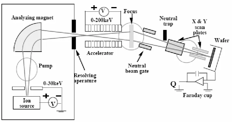
Figure 1-4: Ion implantation schematic.
The major advantage of ion implantation is that it provides a very precise means to introduce a specific dose or number of ions into the substrate. Therefore efficient silicon optical emitters made by ion implantation are preferred.
“One objective of designing an LED must be to achieve a high efficiency. Moreover, the radiation has to have a geometry that allows the optical fibers to collect as much of the optical power as possible, in order to maximize the coupling efficiency. A third objective is to design an LED in which the light output can be directly modulated at high rates with an information-carrying signal by the forward current. Finally, its construction must ensure a rapid discharge of heat from the p-n junction, since the light output drops as the junction temperature rises34.”
This master thesis at the Semiconductor Components group contributes to the HELIOS project at the University of Twente, the Netherlands. Aim of this project is to obtain High Efficiency LIght Emission Out of Silicon.1
In this “literature report”, we report on Light Emitting Diodes made by ion implantation, so called dislocation
engineered. Such a device would also form the basis for the development of an injection laser based on the same principles but with the incorporation of an optical cavity. This master thesis describes how dislocation engineering could increase the (quantum) efficiency.
1
2 Silicon as indirect band gap material and poor quantum efficiency
So aim of this project is to develop efficient silicon Light Emitting Diodes made by ion implantation, so called dislocation engineered.
2.1 Indirect band gap material
An LED is basically a junction diode that operates in forward bias. “From the edge of the depletion layer
electrons will diffuse inward to the metal contact of the p-region while they will slowly recombine with the plentiful holes that are available. At a distance of Ln, the diffusion length of electrons, most of them will have disappeared
and an equal number of holes must come from the contact to supply the holes that have recombined with the incoming electrons34.” Holes go
mutatis mutandis the same way. The only difference is the diffusion length of holes Lp. The diffusion length of holes is approximately 3 times as low as that of electrons.
The amount of recombination decays exponentially from the edges of the depletion layer to the contacts. Therefore most of the surface-emitting LEDs have a thin highly doped n-layer on top with a lowly doped p-layer below35. In that way generated photons are generated not far from the surface and have a high chance of being ejected from the substrate. Besides surface emitters also edge-emitters exist.
Figure 2-1: Junction diode under forward bias (notice the difference in diffusion lengths).
When the metal contacts are placed to close to the edge of the depletion layer, electrons and holes do not have the ‘space’ to recombine in the silicon. Instead some will recombine at the metal contacts. Metals do not exhibit a band gap, and therefore this recombination event will never produce a photon.
“A forward current is passed through a junction diode leads to energy dissipation in the device. This dissipation appears in two forms. The first is Joule heating (the common Ohmic loss, which is not very large in heavily doped neutral regions), which is phonon excitation in the crystal lattice (lattice vibrations) due to collisions of accelerated charge carriers. The second and more important is dissipation due to recombination of carriers in the neutral regions where diffusion takes place (and in the depletion region). The latter form of dissipation can lead to photon generation: carriers recombine crossing the band gap possibly releasing energy in the form of a photon34.” Thus not every recombination event in silicon delivers a photon.
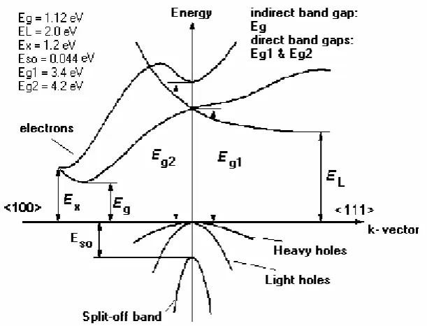
The amount of generated photons is very poor for silicon, because silicon is an indirect band gap material. Most group IV semiconductors including germanium (Ge) and silicon carbide (SiC) are indirect band gap
Figure 2-2: Silicon band structure shows indirect band gap.
However “in semiconductor physics, an indirect band gap is a band gap in which the minimum energy in the conduction band is shifted by a k-vector, which is determined by the material's crystal structure. Semiconductors with an indirect band gap are inefficient at emitting light. This is because any electrons present in the conduction band quickly settle into the energy minimum of that band. Electrons in this minimum require some source of momentum allowing them to overcome the offset and fall into the valence band. Photons have very little momentum compared to this energy offset – hence, the momentum "kick" of a photon being emitted would normally not be enough to dislodge the electron from the conduction band. Since the electron cannot rejoin the valence band by radiative recombination, conduction band electrons typically last quite some time before recombining through less efficient means37.”
An emitted photon is like a bullet leaving a gun. The velocity of the gun being the momentum won’t change. A phonon-assisted momentum “kick” could supply the needed k-vector momentum for photon generation. However energy transfer Ephonon comes along with the momentum “kick”. Setting up a phonon costs energy, while
absorption of a phonon results in energy gain. “It is understood that the transition assisted by phonon emission is more probable due to a negligible amount of phonons suitable for absorption at room temperature18.”
Both a photon and phonon interaction at the same time is unlikely and hence the (quantum) efficiency of indirect band gap semiconductors will be low2. Most of the energy release will not be in the form of a photon. Less efficient means like setting up a phonon dominate. An electron loses bits of energy each time it collides resulting in heat until the electron is no longer excited. An electron that is no longer excited does not have sufficient energy to move free through the material taking part in the conduction. In stead it is a valence electron again possibly taking part in the covalent binding process to keep the material together. The electron recombines with a hole. A hole is an available electron site.
Perfect pure and defect free semiconductors, like semiconductors tabulated in the periodic table of elements, do not permit an electron to reside in the band gap. An electron can only cross the band gap when it has energy exceeding the band gap energy. However impurities or defects introduce extra energy bands called traps or states, in the band gap.
Figure 2-4: Introduction extra energy bands (traps).
Later on we will see that defects called dislocation loops, that are introduced by the implantation process, also introduce energy bands (1D-energy bands). These energy bands help increase the quantum efficiency.
Just as an electron can reside in the valence band or the conduction band, it can also stay in these extra energy bands. An electron does no longer need the band gap energy in order to cross the band gap. It can use these extra energy bands as stepping-stones. Suppose that states are positioned at 1/3 below the conduction band then the largest energy an electron needs is 2/3 of the band gap energy. Therefore the chance that electrons can leave the valence band increases. Both the transition electron band−energy band and energy band−valence band can result in photon emission. Such an emitted photon would result in less energy than the band gap energy! Again phonon and photon action at the same time is required.
2.2 Quantum efficiency
Quantum efficiency is defined as the average number of primary electron hole pairs per incident photon. Primary carriers are generated directly by the incident photon. There is a distinction between the internal quantum efficiency and external quantum efficiency. The internal quantum efficiency is a theoretical value for the average number of primary generated carriers per absorbed photon. An electron generated by a photon might have enough energy to generate a second carrier. The internal gain G grasps this concept. The external quantum efficiency is the measured value for the number of primary generated carriers that are collected at the contacts, per incident photon originating from an external light source. So no internal gain is assumed (G=1). Suppose P0
is the incident optical power in Watts, and Iphoto is the resulting photo current at the contacts in Ampère, then
external quantum efficiency η is defined as35:
2
Equation [2-1]
0
. _
_
_
_
_
&
[ ]
_
_
_
photo
I
No
of
electron hole
pairs
generated
collected
e
P
No of
incident
photons
h
η
υ
=
=
−
Both carriers and photons are influenced by the material boundaries. For example interface trapping of carriers and reflection of light diminish the external quantum efficiency. In general the external quantum efficiency is lower than the internal quantum efficiency. Methods mentioned in the introduction like porous silicon, silicon/silicon dioxide super lattices, silicon nano precipitates in silicon dioxide, erbium in silicon, silicon/
germanium and iron disilicide aim to increase the external quantum efficiency by increasing the internal quantum efficiency. However the external efficiency can also be increased on its own e.g. by process technology like cleaner processes to reduce the amount of surface defects, and proper design3. An example of proper design originates from the solar industry. Solar cells are provided with textured surfaces and mirroring metal layers at the backside9.
Figure 2-5: Textured surface and mirroring metal layers increase quantum efficiency.
Because carrier recombination or generation and reflection are dependent upon photon energy or wavelength, quantum efficiency is also wavelength dependent.
In articles when quantum efficiency is mentioned it is often the external quantum efficiency. The external quantum efficiency of silicon has been estimated 10-6 (about 10-4%)18 i.e. in the best case scenario 1 million
(1,000,000) electrons recombine with as many holes to generate 1 external photon which contributes to the emitted light. Therefore high current values would be required to produce light out of silicon. Conventional LEDs have external efficiencies of 1%, although the internal efficiencies range from 50-80%35. Therefore by saying
“aim of this project is to develop an efficient silicon Light Emitting Diode”, we mean a silicon LED with high
external quantum efficiency in the order of 1%. All quantum efficiencies reported in literature at the moment of writing, concerning “silicon Light Emitting Diode made by ion implantation”, are in the order of 0.1%1,5,6,7.
As mentioned in the introduction, dislocation engineering is not the only way to increase the external quantum efficiency. However we prefer this method based upon ion implantation.
3
3 Increasing the quantum efficiency by dislocation engineering
In this main section we explain how dislocation loops can be engineered, how dislocation loops look like and how the introduction of these loops in junction diodes should increase the quantum efficiency.
3.1 The implantation process and creating excess interstitials
The ion implantation process creates a lot of damage to the silicon substrate. At the same time an excess of interstitials equal to the implant dose is implanted into the substrate. Let us see how this works.
3.1.1 The silicon substrate as starting material
The Light Emitting Diodes are formed using a silicon wafer as substrate. How does this silicon substrate look
like?
Silicon is a crystalline material, meaning that the atoms form regular atomic arrangements. Regions of regular atomic arrangement are called crystals or grains. Each crystal consists of a Unit cell that periodically repeats itself in all directions. The resulting grid is often called matrix.
Figure 3-1: Silicon Unit cell and lattice.
The regular atomic arrangement is called lattice. Each atom resides at its lattice site at 0K.
The forces holding the silicon atoms together to form the lattice are covalent or shared electron bonds. Meaning for silicon that individual atoms prefer to bond with their four nearest neighbors. In a single crystal each
Figure 3-2: Covalent bonding with 4 nearest neighbors.
Single crystalline silicon is used nowadays in the electronics industry i.e. the region of regular atomic
arrangement encloses the total wafer. The figure 3-3 depicts how a simple cubic unit cell, repeated itself in all dimensions. To be clear this is not the actual Unit cell of silicon. However such an abstract mental picture can be useful later on to get some feeling for the ion implantation process and how dislocation loops look like.
Figure 3-3: Model of silicon substrate.
For example, dislocation loops we will discuss later on are intersected extra planes with a loop shape. A plane is a cross-section in a particular direction and consists of the atoms that lie on that plane.
Figure 3-4: Extrinsic dislocation loop revealing inserted extra plane.
Figure 3-5: Grain boundaries destroy regular atomic arrangement.
Grain boundaries are less densely and regularly packed compared to single crystals. Because the regular atomic arrangement is interrupted at the grain boundaries, not each individual atom is able to bond with its four nearest neighbors. The resulting dangling bonds introduce defects. Those have a significant effect on device properties. By following special procedures single crystals wafers are produced with diameters up to 300mm and a typical thickness of 775μm. From this point in text when we speak of silicon we mean single crystal silicon.
The introduction of dislocation loops also interrupts the regular atomic arrangement. The result is again dangling bonds.
3.1.2 Diode junction formation
As mentioned earlier, an LED is a forwarded junction diode. The junction diode can be introduced into the silicon starting substrate by performing a separate diffusion step. Recall that most of the surface-emitting LEDs have a thin highly doped n-layer on top with a lowly doped p-layer below. In that way generated photons are generated not far from the surface and have a high chance of being ejected from the substrate.
Figure 3-6: N-type silicon on top of p-type silicon.
A straight forward design results in n-type dopant and p-type silicon substrate. However as indicated in the introduction, conventional LED construction must ensure a rapid discharge of heat from the p-n junction, since the light output drops as the junction temperature rises. Therefore in conventional LED design, the silicon substrate is n-type and the dopant is p-type. The n-type substrate is fitted upside down on the heat sink i.e. the substrate is flipped. And finally a hole has been etched away in the substrate at the light output side, so that the light only has to travel through a thin n-type layer35.
3.1.3 The implantation process and damage accumulation
The dislocation loops are introduced into the silicon substrate by ion implantation. The implantation process is not treated in detail, because it is such a common process in IC-processing. Our summary is extracted from reference 33.
The implantation process consists of the acceleration of ions, targeting them at the silicon substrate, and implanting them in it. Channeling occurs often in crystalline silicon.
Figure 3-7: Artist impression of channel.
The small-angle scattering events from the atoms that line the walls of the channel results in ions that are steered quite a long distance along the channel before coming to rest from the electronic drag or from a sharp nuclear collision that causes the ion to exit the channel. Due to scattering events each implanted ion follows a random trajectory.
Figure 3-8: Scattering events.
Since the total number of ions implanted is usually greater than 1012cm-2, the distribution can be described
Equation [3-1]
( )
(
)
( )
2 2
2 2
[
]
p p
x R
p
n x
n e
σcm
⎛− − ⎞
⎜ ⎟
⎜ ⎟
⎜ ⎟ −
⎝ ⎠
=
Rp is the average projected range normal to the surface, σp is the standard deviation about that range, and n(Rp)
is the peak concentration where the Gaussian is centered. Besides a distribution in projected range, a distribution in lateral range, called lateral straggle σ⊥ exists. However we only concern our self with the distribution in projected range.
Figure 3-9: Projected range, peak concentration and standard deviation.
Note that the actual distribution profile in projected range can deviate from the Gaussian profile. For example the effect of channeling on the implant profile is to cause a tail that continues much further than expected. Also lighter ions do have the tendency to back scatter of silicon atoms and fill in the front side of the distribution. Therefore less simple models exist taking into account all kind of aspects.
A convenient relationship between dose, peak concentration and standard deviation about that peak concentration, can simply be derived by integrating equation 3-2:
Equation [3-2]
( )
22
p p[
Q
n x
x
πσ
n cm
∞
− −∞
With known dose and implantation energy, the standard deviation and projected range can be found in look-up tables (Appendix B − look-up table projected range and standard deviation most common dopants in silicon). With help of equation 3-2 the peak concentration can be calculated.
Later on we will see that if the implant concentration is within 10% of the silicon concentration, the silicon is regarded as amorphous. Amorphous material lost all its regular atomic arrangement due to the ion
bombardment.
3.1.4 Dose, damage and defect production
The scattering events that an implanted ion encounters can be divided into nuclear collisions and electronic stopping. Sharp nuclear collisions result in displacements of silicon atoms from the lattice sites. An atom or ion that does not reside at a lattice site, whether it is the displaced silicon atom or the implanted ion, is called interstitial. A silicon atom displaced from its own lattice site is called self-interstitial. The vacant lattice site is called vacancy. The lattice positions are such that the free energy is minimized39.
When an interstitial is injected into the lattice, considerable energy is expended and the lattice becomes strained. Therefore the energy which is required to move the interstitial is low and they can easily migrate to energy sinks. Sinks can include the surface, interfaces or other vacancies or interstitials. Also impurity ions/atoms both in lattice and interstitial positions can act as a sink for lattice defects and can promote defect clustering processes. Interstitial positions are matrix places between lattice sites39.
If the nuclear collision does not separate the self-interstitial and vacancy for enough, they will immediately recombine again. However when an amount of energy, called the displacement energy is put into the nuclear collision, a stable self-interstitial-vacancy pair is formed. Such a pair is called Frenkel-pair12.
Figure 3-10: Displacement energy and Frenkel-pair generation.
For silicon the displacement energy is approximately 15eV. The implant energy En is often in the range of kilo
electron volts (1−1000keV), therefore a large number of displacements will be caused. A sequence of
displacements is called cascade. An estimate for the number of displaced atoms is given by the Kinchin-Pease-formula33:
Equation [3-3]
2
n d
E
d
E
=
Thus per implanted ion, depending upon the implantation energy, a large amount of Frenkel-pairs is generated. A large amount of interstitials and vacancies are injected into the matrix. When interstitials or vacancies
clusters, dopant-defect complexes and some isolated interstitials and vacancies. The recombination of a vacancy and interstitial restores the lattice-order.
The question now is how this primary damage introduced by 1 implanted ion accumulates when other ions are implanted. Some of the defects generated can recombine with defects from other cascades.
3.1.5 The implantation dose and realization of an amorphous layer
Physically, the dense damage cascades from heavy species like arsenic allow for more efficient recombination than the more dispersed damage distribution from a light ion like boron. Overlapping cascades locally increase the amount of displaced atoms until amorphous pockets arise. If the dose is high enough the primary damage builds up until eventually an amorphous state is reached33.
Table 3-1: Damage versus implant dose39.
The threshold for amorphous layer production is the total vacancy concentration above which the substrate is assumed to be amorphous. It is expressed as a percentage of the silicon atom concentration33. The silicon atom
concentration is 5 1022cm-3. Usually this threshold is assumed to be 10%. Remember from figure 3-9 that the peak concentration np exceeds this threshold first.
3.1.6 Amorphous layer evolution dependence upon ion mass and implant energy
Whether an amorphous layer is formed is almost exclusively dictated by the implant dose. However the subsequent evolution of the amorphous layer depends upon the implanted atom/ion mass and implantation energy.
For heavy ions like arsenic, whose stopping may be dominated by nuclear collisions, the damage profile is relatively flat over the whole projected range up to Rp i.e. from surface to projected range atoms have been
displaced. Lighter ions like boron have an appreciable component of electronic stopping at higher energies. Electronic stopping does not result in displacement of atoms. Therefore the damage accumulation is
concentrated near Rp i.e. atoms are only displaced near Rp. For lighter ions then, the amorphous region will form
first at the peak of the damage density profile near Rp and expand on both sides of this depth as the implant
Figure 3-11: Evolution of amorphous layer.
In general simply up scaling up a low-dose implant does not give the same profile as a high-dose implant. As the crystal is damaged by the implanted ions, channels are less evident to subsequent incoming ions. Relatively speaking, higher implanted doses are less prone to channeling effects. Producing an amorphous layer before the actual ion implantation, called pre-amorphization, eliminates the effect of channeling33.
It is also worth mentioning that it is easier to form an amorphous layer at low temperatures (liquid nitrogen) rather than at room temperature or higher. This observation is easily explained by the larger fraction of ions that recombine within a cascade at higher implant temperatures. If the implant is performed at liquid nitrogen temperatures rather than room temperature, a lower implant dose can be used to form the same amorphous layer. Because of this, the amount or dose of damage in the tail of the damage distribution beyond the a/c interface is much less for the liquid nitrogen temperature implant. Also the a/c interface is sharper33.
3.2 The implantation dose and nucleation of dominant defects
During the ion implantation, various levels of damage can be done to the lattice. The resulting defects depend almost entirely upon the implantation dose (implantation energy 40−200keV)21. For silicon implants in silicon
these levels of damage can be divided into five regimes:
Table 3-2: Damage regimes versus implant dose.
Implanted silicon dose [cm-2] amorphous
implant Depth of defect formation Defect
A <5×10¹² 1×10¹¹−2×10¹³ No − Nanometer-size Interstitial
clusters B 5×10¹²−1×10¹⁴ 2×10¹³−1×10¹⁴ No − Intermediate Defect
Configurations = rod-like defects and {113} stacking faults
C 2×10¹⁴−1×10¹⁵ No Projected
range Rp
Category I: Intermediate Defect Configurations, Frank stacking
faults and perfect prismatic dislocation loops
D >1×10¹⁵ Yes End of Range
(EOR) region
Category II: Intermediate Defect Configurations, Faulted loops and perfect prismatic dislocation
loops
E >2×10¹⁵ Yes − Dislocation networks
(a) “At silicon implantation doses below 5×1012cm-2, no {113} defects are observed. This could indicate that the
interstitial clusters formed from the implantation damage, are too small to be detected by Transmission Electron Microscopy. Alternatively, this threshold dose could reflect a nucleation barrier for the formation
and growth of {311} defects40”. “Recently, Crowern and co-workers have been able to extract information on
(700°C) and for times from 15s up to 40 minutes after low-dose implants (1×10¹¹−2×10¹³ Si/cm2)10”. Also,
“tight-binding calculations of I-agglomeration revealed that the structure of an I-cluster alternative to the {311} defect structure may exist when few interstitials agglomerate. The formation energy per I is lower than that necessary for the formation of the (110) chain, which is the building block of the {311} defect, when the number of interstitials is lower than 10.10”
(b) The point defects left over after recombination of vacancies and interstitials will be dominantly interstitial clusters. The point defects coalescence into what has been termed Intermediate Defect Configurations (IDCs). They include rod like defects as well as {113} stacking faults (also called {311} rod-like defects)2.
“For doses in between 5×10¹² and 1×1014cm-2, {311} defects are the only visible defects40”. After using both
Deep Level Transient Spectroscopy (DLTS) measurements and Photoluminescence (PL), Libertino points out “the strong reduction in the defect concentration at 5×1013cm-2, about one order of magnitude, can be
attributed to the formation of extended {311} defects, obtained at fluences above 2×1013cm-2…10”.
Intermediate Defect Configurations are part of category I damage, but not exclusively. Category 1 damage forms when the implantation damage is insufficient to produce an amorphous layer. Like the name
“intermediate” suggest, these defects might transform into more stable defects e.g. extrinsic Frank stacking faults loops and perfect prismatic dislocation loops, if the implant dose and subsequent thermal budget is right. The interstitials left over after high temperature anneals, will coalescence into loops. These loops are extra planes consisting of self-interstitials.
“Extended defects or dislocation loops will result if the dose or peak concentration is above a critical concentration. For doses below 2×1014cm-2 no dislocation loops were observed. This corresponds to a
critical peak concentration of ~1.6×1019cm-3. This critical concentration is independent of the species and
wafer orientation2”. The category 1 defects form at the projected range
Rp.
This critical peak concentration is related to the (electrical) solid solubility of silicon. Implanted ions are not yet part of the crystal structure. Annealing provides energy to bond with 4 silicon atoms in the
re-crystallizing structure, thereby occupying a lattice site. The implanted ion is said to become electrically active. At the same time a self-interstitial is created giving up its lattice site. At some depth like the
projected range or later on discussed end-of-range region, the concentration of implanted ions first exceeds the electrical solid solubility. The electrical solid solubility reflects the amount of foreign atoms that can be incorporated on lattice sites by ejecting a self-interstitial. When the electrical solid solubility is exceeded implanted ions start to occupy interstitial sites i.e. matrix space between lattice sites, and start forming neutral clusters. When even the solid solubility is exceeded a separate phase is formed e.g. an extra plane. The extra planes provide new available space in the form of (lattice) sites. The self-interstitials created by ion implantation gather to occupy these extra planes. These extra planes often have the shape of loops33.
(c) A typical category I dose regime for silicon implants is 2×10¹⁴−1×1015cm-2. Above a threshold dose of
2×1014cm-2, {113} defects break up22. After dissolution of {113} defects an excess of interstitials provide the
formation of extrinsic Frank stacking fault loops (also called Frank loops or faulted loops) and perfect prismatic dislocations loops (often called perfect loops). Since these dislocations are more stable than {113} defects, significantly stronger annealing steps are needed to fully dissolve this dislocation damage.
It is not possible to produce category I extended defects by room temperature or lower temperature for implantation with heavier ions such as arsenic. Category I damage forms when the implantation damage is insufficient to produce an amorphous layer. The production of an amorphous layer takes place at an implant dose of 5×1013cm-2 for implants with implantation energy below 200keV. So an amorphous layer
forms first and therefore category II defects, that forms when the damage is sufficient to produce an amorphous layer, is produced prior to exceeding the critical peak concentration necessary for category 1 defect formation2.
Figure 3-12: CategoryI and II damage for varying ion mass and implant dose.
(d) For silicon the implantation dose should exceed 1×1015cm-2 to produce category II defects22. Category II
damage forms when the implantation damage is sufficient to produce an amorphous layer.
Let us start with an example that illustrates the influence of the proximity of the surface upon category II defects nucleation.
IMEL-NCSR “demokritos”15 reports in her Bi-annual report 2001-2002 that the proximity of the silicon surface to the dislocation loop band (on the order of 5 nm), causes the dissolution
of category II defectseven from the early stage of the oxidation process. Extended defects were absent after dry oxidation of nitrogen implanted silicon (3keV, 1×1015cm-2) at 800°C for 60 minutes.
All defects, whether it are {311} rod-like defects, Frank stacking faults or perfect loops, consist of interstitials due to the nature of the implantation process. The surface loss of interstitials is too high when the surface is to close to the defect region. Consequently defects dissolve before they nucleate. We assume that surface loss is negligible.
The implantation process gives rise to large amounts of displaced atoms or interstitials, even after
Figure 3-13: End-of-range region and depth of a/c interface.
“The area under the damage density distribution beyond the a/c interface does not increase with higher dose due to the increase in thickness of the amorphous layer with dose2”.
Due to the presence of large amounts of interstitials in this region it becomes stretched. However the Solid Phase Epitaxy (SPE) re-grown silicon is not stretched. Therefore, high stress exists at the
amorphous-crystalline interface. To relieve stress, interstitials just beyond the amorphous-amorphous-crystalline interface form dislocation loops2.
Upon annealing, type II (end of range) dislocation loops e.g. faulted or perfect are observed to form. The formation of extrinsic dislocation loops in the category 2 region is energetically favorable to the formation of a large cluster of interstitials like {113} stacking faults. The reduction in strain energy associated with the formation of an extra plane is larger. The evolution of category 2 damage from point defects to extrinsic dislocation loops during annealing, is believed to occur via intermediate defect configurations such as {113} stacking faults2.
Thus, once again, due to the stress, clusters like {113} stacking faults, are less preferred than category II loops. Remember that category I loops form in the absence of an amorphous layer and resulting stress. Therefore the ratio {113} stacking faults to category I loops will be lower than the ratio {113} stacking faults to category II loops.
(e) if the concentration of atoms bound by the extrinsic dislocation loops exceeds the concentration of atoms in a mono layer of the {111} plane of silicon (~1.4×1015cm-2), then dislocation network formation becomes
possible upon annealing via dislocation-dislocation interaction2.
After dissolution of {113} defects an excess of interstitials provide the formation of Frank- and perfect loops. However, some of these interstitials diffuse into the bulk or surface. Therefore the dose necessary for dislocation network formation has been estimated 2×1015cm-2 which is higher than ~1.4×1015cm-2.
In the dose regime above 1.4×1015cm-2 some remarkable aspects concerning the roll of pre-amorphization
Table 3-3: Roll of pre-amorphization from Jones experiment.
Pre-amorphization implant Implant
Energy Dose Energy Dose
Jones Experiment
E Q E Q
Sample keV cm-2 keV cm-2
1 − − 50 1×10¹⁶
2 70 5×10¹⁵ 30 5×10¹⁵
3 30 5×10¹⁵ 70 5×10¹⁵
After re-growth of the amorphous layer at 550°C, the samples were annealed at 900°C for 16h. When compared with sample 1, the concentration of atoms bound by the dislocation loops is observed to be smaller for sample 2. However the concentration of atoms bound by the dislocation loops is observed to be larger for sample 3.
Thus a low energy pre-amorphization implant followed by a higher energy implant introducing the same dose as a single implant, results in a larger concentration of atoms bound by the dislocation loops.
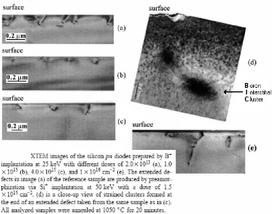
An interesting situation exists when a pre-amorphization implant with silicon atoms is followed by a high dose boron implant. At boron implants exceeding 1×1016cm-2, the boron concentration reaches the thermal
equilibrium solubility limit (1.53×1020cm-3) at 1050°C14. Hence the boron clusters can not be dissolved
during the long time anneal. “Observations by Cowern et al. [9, 10], suggest that in systems where B is present in large doses, excess interstitials help boron atoms to form boron clusters and are themselves incorporated into these clusters (so-called Boron Interstitial Clusters, BICs)21”. Sun et al. suspect that the dark spots depicted in figure 3-1414 are the BICs, however they were not able to prove it. The origin of the
contrast of these dark spots is attributed to high strain in an area of locally high density of Si-B interstitial clusters, Si interstitials, or it is induced by the strain field around extended defects (like dislocation loops)14.
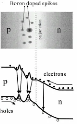
Later on more about how the introduced dislocation loops and “doping spikes” help increasing the quantum efficiency. Because increasing the quantum efficiency is what we try to achieve. For now we can mention that both dislocation loops and doping spikes act as blocking potential, thereby hindering the motion of carriers across the junction, figure 3-1514.
Figure 3-15: Boron interstitial clusters act as transition barrier for carriers.
The carriers are confined to the region where the blocking potentials are situated.
We chose to introduce the dopant and dislocation loops in 2 separate steps. Dislocation loops are
introduced by silicon ion implantation after the junction has already been formed by in diffusing. Advantage is better control, however the disadvantage is the lack of “doping spikes” that help block the carriers and consequently improve the quantum efficiency.
3.3 Annealing and evolution of dominant defects
The right dose provides the nucleation of different types of defects during annealing. The evolution of these defect nuclei depends on the thermal budget. Annealing takes place in an inert ambient unless stated otherwise.
The evolution of both category I and category II damage from point defects to respectively category I and category II loops upon annealing, is believed to occur via intermediate defect configurations such as {113} stacking faults. The implant damage is removed during a typical re-crystallization temperature of 550°C.
What remains is the category I or category II damage. For different thermal budgets, different defects will evolve. Eventually for sufficient high thermal budgets all defects dissolve.
Table 3-4: Regimes during thermal annealing.
Annealing
Temperature regime °C {311}
Rod-like loops
{311} Rod-like defect and loop activity
<700 Growth Growth {311} Rod-like defects nucleate and grow by capturing interstitials. {311} defects form the nuclei of perfect loops. 700−800 Dissolution Growth {311] Rod-like defects dissolve by releasing interstitials. Perfect
loops continue to grow by capturing interstitials. Frank loops nucleate and start growing.
800−900 − Coarsening Both perfect loops and Frank loops enter Oswald rippening process: average loop radius increases while average loop density decreases. The total amount of interstitials bound by the loops stays almost constant
900−1000 − Coarsening/
Dissolution Oswald rippening process continuous and at the same time some loops dissolve by releasing interstitials. The total amount of interstitials bound by the loops decreases.
>1000 − Dissolution All loops dissolve by releasing interstitials.
The first defects that start evolving (besides the nanometer-sized Interstitial clusters) are the {311] defects. It is shown that {311} rod-like defects have three stages of micro-structural evolution3:
• Accumulation of point defects to form circular interstitial clusters; • Growth of these circular clusters along the <110> direction; • Dissolution into the silicon matrix.
Intermediate Defect Configurations were estimated to be ~20A2. {311} Defects start breaking up for
temperatures over 700°C i.e. they dissolve into the silicon matrix. During this dissolution process interstitials are gradually lost from the damage region through diffusion into the bulk and to the surface, the latter most likely being the dominant loss mechanism. The rate at which this decay occurs is determined by the average binding energy of interstitials at {311} defects (1.3eV), the proximity of the surface, and the initial interstitial
concentration as it is set by the implant dose.
The dissolution of {113} defects provides an excess of interstitials that allows the formation of category I or category II loops, depending on the exact implant dose. Dislocation loops nucleate, upon annealing, from primary defects residing in the crystalline silicon near the amorphous/ crystalline interface. A certain critical dose (2×1014cm-2) must be used in order to form stable loops [24]. Otherwise dislocations cannot exceed critical
dimensions for stable growth due to lack of point defects from the implant. In this case, unstable loops nucleate but dissolve upon annealing19. For a thermodynamic explanation of dislocation nucleation, the reader is referred to the model proposed by Tan30.
For the following information we should point out to references 22, 23 or 25, unless stated other wise.
For the 2×1014cm-2 dose, which is below the amorphization threshold, the dominant defect at 700°C is the {311}
defect with a much smaller concentration of type I loops. The total trapped interstitial concentration was around 7×1013cm-2 for 700°C 1 hour anneals. The formation of category I loops does not result in complete trapping of
Figure 3-17: Ratio {113} defects to category I loops (2:1).
For the 1×1015cm-2 sample amorphization occurs and both type II (end of range) loops i.e. extrinsic Frank
stacking fault and perfect prismatic loops, and {311} defects are observed for 700°C anneals. The total number of trapped interstitials for 700°C 1 hour anneals is also around 7×1013cm-2. The ratio, total amount of
interstitials: {311} defect: type II loops is 7:2:5. Thus the ratio of {311} defects to loops has switched such that the dominant defect is the type II loop. Upon annealing, the {311} defects again show a reduced dissolution rate and the type II loops are in the growth regime. Increasing the anneal temperature to 800°C results in further growth of the type II loops and all of the {311} defects have either dissolved or unfaulted.
Figure 3-18: Ratio {113} defects to category II loops (2:5).
The light emission has been assigned to the category I and category II loops. The total amount of trapped interstitials is for both category I and category II loops the same. However the ratio {113} defects to category I loops (2:1) is much smaller than the ratio {113} defects to category II loops (2:5). Or in other words, a higher percentage of the implant dose directly results in loops for an amorphous implant. At 800°C most {311} defects dissolved. During their dissolution the injected interstitials provide the nucleation and growth of Frank loops and further growth of perfect loops. However interstitials are lost during the dissolution process. These interstitials don’t end up in loops. For amorphous implants a higher percentage of the implant dose directly results in loops, and these interstitials can’t get lost during {311} dissolution. Therefore from this point in text we examine category II loops.
Figure 3-192 depicts the amount of interstitials bounded by the category II loops as function of the implant dose. In is interesting to see that the amount of atoms bound by the dislocation loops is larger for heavier implant species.
Figure 3-19: Bound interstitials versus implant dose (increase for heavier species).
During annealing, a coarsening process known as Ostwald ripening takes place, resulting in the growth of large loops at the expense of smaller ones, figure 3-20.
Figure 3-20: Oswald rippening process (f= Frank loop, p= perfect loop).
Therefore during the Oswald rippening process, the total amount of interstitials bounded or trapped by the loops remains almost constant. Bonafos et al. give a thorough analysis of this process31.
The loop growth rate is approximately constant for each annealing temperature (700−1000°C).
Figure 3-22: Category II loop growth rate (almost constant versus temperature).
The loop growth is governed by the bulk-diffusion mechanism. According to bulk diffusion mechanism, the radii of growing loops are proportional to the annealing time. This implies an uniformly increasing average loop radii. In addition, the loop growth rates increase with the increase of annealing temperature. At lower temperatures (700°C, 800°C) this growth appears to be much slower than that at high temperatures (900°C, 1000°C). The average loop radius for 1000°C anneal is much larger than that of the other temperatures. In general, secondary defects become large enough to observe via transmission electron microscopy (TEM) during post implantation annealing at temperatures exceeding 700°C.
Figure 3-23: Loop radius increases and loop density decreases during Oswald rippening.
In the mean time the total loop density is decreasing (larger loops grow at the expense of smaller loops) which makes the density of interstitial bound by the loops stay constant for low temperature annealing and decrease after annealing at high temperatures (i.e. ≥900°C). For 700°C and 800°C annealing, the loops remain in the coarsening regime (for annealing times up to 16 hours) and the density of the interstitials bound by the loops is constant during the annealing process. For 900°C annealing, after 30 minutes the interstitial density decreases and the loops change from the coarsening regime to the dissolution regime. After only 15 minutes annealing at 1000°C, the loop dissolution process starts and the interstitial density reaches a very small value (< 3×1012cm-2)
after 2 hours. For annealing times greater than 2 hours at 1000°C, very few loops remain and they evolve into stacking faults.
It appears that the magnitude of the strain is sensitive only to the anneal temperature for temperatures below 900°C. At elevated temperatures (>900°C), it is a strong function of both the annealing time and temperature”18.
Figure 3-24: Strain almost constant during Oswald rippening (decrease during dissolution).
Pan et. al. divides the category II loops into Frank loops and perfect to show both density and mean loop radius of both type of loops.
Figure 3-25: Frank curves follow perfect loop curves (evidence of no unfaulting of Frank loops).
Both dislocation loops grow simultaneously with anneal time. In addition, the density-time curve for the Frank loops closely follows the density and mean radius curves for the prismatic loops. This suggests that the
increase of interstitials for prismatic loops and the decrease of interstitials for Frank loops with annealing time is a preferred ripening of prismatic loops rather than an unfaulting effect of Frank loops.
In addition Pan et. al reveal the damage distribution profiles of both Frank loops and perfect loops.
“A study of End-Of-Range (EOR) dislocation loops in silicon implanted with 50keV 1×1016cm-2 was carried out
by using transmission electron microscopy. The size distribution profile of faulted Frank dislocation loops could be well fitted by a normal Gaussian probability function and that of perfect prismatic dislocation loops by a log-normal Gaussian probability function”
Figure 3-27: Difference in distribution function (notice the tail for perfect loops).
Authors assign optimum light emission to annealing temperatures varying between 975−1100°C, with an average of 1050°C and annealing times around 20 minutes, at least for boron implants. Due to the coarsening the average loop radius is much larger and the density is much lower after 1000°C anneal than for lower temperature anneals. Some “rare authors” assign the light emission to the perfect prismatic loops, because for a silicon implant the radius of perfect loops is largest. According to reference 4, the average loop radius, which is an indicator of how large the loops are, is important in relating the spread of the strain in the lattice. The larger the loop, the larger is the length of the strained lattice. The larger strained lattice contributes to the improved potential barrier, which is the reason for the increased intensity.
Kase and Liebert17 et. al. support this relation, loop size-light intensity, although they approach it from a slightly different angle. They keep the thermal budget the same, but performed boron implants at different implant temperatures: liquid nitrogen temperature (NT), -60°C and room temperature (RT), and established density and size of the loops and resulting leakage current. The leakage current is related to the amount of recombination that takes place.
They conclude “the higher concentration of loops at -60°C than at RT does not correlate with JR. On the
contrary, JR at LN temperature is not reduced. We cannot explain this at this time, but we assume that the large
dislocation loop in Fig. 1 (c) may be concerned with large JR.”
Reference 3 reveals that “Meng et al. investigated the interaction between oxidation induced point defects i.e. injected interstitials during oxidation, and dislocation loops.”
Figure 3-28: Dry oxygen and inert annealing ambient (notice increased loop radius for oxygen).
Annealing in a dry oxygen ambient results in 2.5(!) times larger average loop radius in comparison with
annealing in an inert ambient for 1×1015cm-2 implant dose. When the recombination rate correlates with average
loop radius, then performing the annealing step in an oxidizing environment might not be a bad idea for implant doses around 1×1015cm-2. Figure 3-28 reveals us that the average loop radius is almost independent of implant
dose for annealing in dry oxygen ambient. Figure 3-19 shows us that the amount of interstitials bounded by the loops is directly proportional to the implant dose. Therefore an implant dose that exceeds around 3×1015cm-2
must be followed by an inert anneal.
However Sobolev6 et. al. argues that the optimum light intensity on average happens for annealing budgets (~1050°C for 20 minutes) that must result in the dissolution of loops. Therefore the remaining implant damage after Solid Phase Epitaxy re-growth and dissolution of the loops is responsible for the light emission, not the loops themselves: “The dislocation loops are found to dominate after annealing at 1000°C, as in paper [1], but they do not produce the maximum quantum efficiency. The maximum ηint and τp are observed after annealing at
1100°C, when the extended defects are not introduced…The influence of extended defects on the band-to-band luminescence is most likely to be related to the gettering of radiation-induced non-radiative recombination centers and/ or the introduction of new recombination centers.”
ηintIs the internal quantum efficiency, andτpis the minority carrier lifetime.
3.4 The dominant defects introduced by the implantation process: {311} Rod-like
defects, Frank faulted loops and perfect prismatic loops
This information became available through extensive mail correspondence with the first author of references 27 and 28, L. Fedina.
Therefore some authors like L. Fedina, believe the term "extrinsic" is a wrong one because both self-interstitial atoms and vacancies are native point defects i.e. intrinsic in nature. This mistake historically came from the situation when the nature of interstitial type Frank loops could not be determined exactly. They thought that this defect was introduced by agglomeration of foreign atoms meaning of extrinsic in nature. However, the term "extrinsic" is still in use nowadays in literature, but it means only "interstitial". In addition, it has been shown that rod-like defects do not exclusively consist of self-interstitials.
The defects should be separated not only as "extrinsic" and "intrinsic", but rather as "gliding" defects and “prismatic” defects.
3.4.1 Gliding dislocations
Gliding dislocations like 30° and 90°-partial Shockley (a/6<112>) or 60° (a/2<110>)- dislocations are always "intrinsic". They can never be "extrinsic", and they never include vacancy aggregation. Gliding defects form without any movement of point defects. This dislocation is introduced to relieve the local strains of the crystal: by plastic deformation e.g. during hetero-epitaxial growth of films on foreign substrates (silicon on Germanium)
Figure 3-29: Lattice mismatch result in gliding dislocations.
Figure 3-30: Shockley gliding is small displacement of host atoms.
Gliding of dislocation is bond switching followed with small displacement of host atoms within the vector of lattice translation. This Burgers vector always shows the direction of displacement of the crystal. The Burgers vector of gliding dislocations is always lying on the defect plane. Thus no additional extra layer is created after gliding. The displacement-angle is the angle between the defect plane and the Burgess-vector.
3.4.2 Prismatic dislocations
"prismatic" dislocations form during aggregation of point defects e.g. due to the implantation process.
Aggregation of (self) interstitials results in “extrinsic” prismatic dislocation loops and aggregation of vacancies results in “intrinsic” prismatic dislocation loops.
Figure 3-31: Intrinsic and extrinsic character of dislocation loops.
The term "prismatic" comes from the fact that the Burgers vector never lies on the defect plane. The displacement angle is 90° with respect to a Frank defect plane (a/3<111>) or 60° with respect to a perfect prismatic dislocation loop plane (a/2<110>). Prismatic defects exist mainly in the shape of LOOPS
3.4.3 {311} Rod-like defects
Figure 3-32: {311} Type defects for the weak beam dark field imaging condition19.
It is believed that interstitials form chains along <110> direction and these chains come together to form a {113} plane. This defect can get very long (about 1µm) in the <110> direction, hence is given the name “rod-like” defects21.
Figure 3-33: Formation of long interstitial chains on <311> plane in <110> direction33.
There is a final equilibrium structure that is Takeda's structure29.
Figure 3-34: Cross-section of {311} rod-like defect (I-dimers = interstitial chains that form extra “virtual” plane, and 5-7 rings surround extra plane to relieve stress).
5-7-Ring defects are associated with strain relaxation. The distance between the “virtual” extra {113} plane and the 2 {113} lattice planes it lies between equals the burgess vector. The burgess vector is a/25<116>=0.14nm. In contrast to dislocation loops, these I-dimers chains are surrounded by a distorted crystal structure. The recent claim of G.Z. Pan et al. that “ {113} defects other than dislocation loops result in strong silicon light emissions.” 33, might be linked to this distortion of the crystal structure.
The final structure of complex point defect clusters mainly depends on 2 aspects:
• The competition in point defect recombination rate at the cluster i.e. restoration of covalent bonds with corresponding bond lengths and bond angles. The recombination rate depends mainly on the temperature; • The rate of additional point defect arrival at the cluster. Point defect arrival depends mainly on the local point defect super saturation.
High super saturation of point defects is needed for {113} defect to grow in <110> direction. A high density of nuclei strongly decreases the super saturation and inhibits the growth.
3.4.4 Frank faulted loops
Figure 3-35: Frank stacking fault loops (notice these loops look like lips).
A full extra plane is inserted between 2 {111} layers27.
Figure 3-36: Extra Frank stacking fault plane (under HREM conditions) introduces many 5-7 rings near dislocation loop boundary to relieve stress.
Figure 3-37: Principle of twin layer12.
Dark spots in the HREM image correspond to projection of atomic chains in the [110] direction, and white spots are the channels along the [110] direction in the silicon lattice. The dark spots located at the extra plane are rotated (according to their twin position) with respect to dark spots far from the defect. Another layer of rotated dark spots is placed at the top of the extra plane. From the HREM it is clear that the interstitials that form the extra plane do not occupy lattice positions. Thus the Frank faulted loop (also called Frank stacking fault) is accompanied by a stacking fault, hence its name.
The extra plane bonds with the twin interface from one side (accompanied by Shockley gliding) and from the other side by an additional stacking fault in the form of Shockley gliding (creating the second twin interface). The Burgess vector of this extra plane is a/3<111>=0.314nm and equals the distance between the extra {111} plane in the center of the Frank stacking fault and the {111} lattice planes it lies between.
5-7-Rings are created only at the loop boundary (the core) with a thickness of about 0.3nm. In figure 3-36 many 5-7-rings are depicted. The HREM condition helps to reveal 5-7-rings by stress relaxation. However for Frank stacking faults under “normal” conditions just one 5-7-ring exists at each side of the loop boundary. At this loop boundary the strain is highest. 5-7-Ring defects are associated with strain relaxation. The energy of the core decreases due to a smaller Burgers vector of 5-7-ring defects a/5<111>= 0.191nm compared to the center of the loops, a/3<111>=0.314nm. Strain energy is proportional to the square of the Burgers vector.
3.4.5 Perfect prismatic loops
A full extra lattice plane is shifted between 2 {111} planes, but not in twin position. Therefore each interstitial on the {111} plane occupies a lattice site. Therefore this defect is not accompanied by a stacking fault. The
distance between the extra plane and the 2 lattice planes is equal to the