ISSN(Online): 2320-9801
ISSN (Print) : 2320-9798
I
nternational
J
ournal of
I
nnovative
R
esearch in
C
omputer
and
C
ommunication
E
ngineering
(An ISO 3297: 2007 Certified Organization)
Vol. 4, Issue 7, July 2016
A Low Noise, Voltage Control Ring Oscillator
Based on Pass Transistor Delay Cell
Devi Singh Baghel1, R.C. Gurjar2
M.Tech Student, Department of Electronics and Instrumentation, Shri G.S. Institute of Technology and Science,
Indore, India1
Asst. Professor, Department of Electronics and Instrumentation, Shri G.S. Institute of Technology and Science, Indore,
India2
ABSTRACT: Voltage control ring oscillators are the heart of communication system. They are widely used in PLL for frequency synthesize. This paper presents the design of low noise voltage control ring oscillator in 0.18µm CMOS technology for the application ofFM radio telecommunication (88MHz-108MHz).The proposed design consists of five delay cell stages. The output Frequency tuning range is 71MHz-112MHz and Control voltage varies from 0V to 0.8V. The proposed voltage control ring oscillator (VCRO) achieves a phase noise of -117.92dBc/Hz at a 1 MHz offset frequency. We have used the inverter based pass transistor delay cell technique to improve linear characteristics and to decrease thepower dissipation of the designed circuit. We have also used NMOS as active resister load to improve the phase noise. The supply voltage (Vdd) used is 0.8V and the maximum power consumption is 317.2 µW.
KEYWORDS: Oscillator, Power Consumption, Phase noise, Frequency tuning, Delay cell, VCO.
I. INTRODUCTION
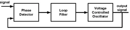
Every communication system transmits and receives data from the other transceiver system. For this the system has to work on certain frequency. Fig. 1 is the block diagram of PLL. Phase locked loops (PLL) are used to generate and synthesize that required frequency for the communication system [1]. Voltage control oscillator generates the required frequency for the PLL block and thus VCOs are the main frequency generating units for PLL.Phase detector detects the phase of input signal and compares it with the output phase of the VCO. Hence changes the output of the loop filter .Voltage control oscillator generates the output frequency according to the voltage generated by theloop filter unit. PLL is generally used as a clock recovery circuit. There are mainly two types of oscillators. Inductor capacitor based VCOs and Ring VCOs. Ring VCO consumes smaller layout area and lower power dissipation. Ring oscillators are having less design complexity and they provide wide tuning range [9]. These days’ ring VCOs are also implemented on two topologies these are single ended ring VCO and Differential ended ring VCO. Differential ring oscillator typically requires more power consumption and chip area size compared to single ended ring VCOs [2].
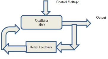
Fig. 2 Delayed feedback oscillation
However a modern communication system widely uses system on chip. That is because of its compactness and lower power dissipation and thus in order to take these advantages it is difficult to design inductor and capacitor based VCOs on the semiconductor chip.Taking about ring VCOs these are quite good because they are not having any on chip inductor or capacitor. Thus we have designed single ended inverter based ring oscillator. Periodic output signal can be generated by the oscillator with respect to control voltage. A simple oscillatory system can be seen in Fig 2. It shows the oscillatory feedback system. For sustain oscillation the oscillatory system must follow the Barkhausen’s stability criteria and should became sustain periodic signal[2]. According to Barkhausen’s criteria two condition must be simultaneously satisfy for sustain oscillation that are the loop gain must be unity and total phase shift around the loop must be equal to zero or 360˚.
II. RELATED WORK
In [2] the proposed VCO is based on single ended delay cell topology. It is an inverter based VCO which uses single ended type of delay cells. This is four stage VCO which operates from 12.6MHz to 48MHz. It gives full swing, wide tuning range and can operate at both high and low frequency mode. Reference [2]uses 1 V as power supply and its topology reduces the static power dissipation. Higher amplifier trans-conductancecan be achieved through its current reuse technique. The maximum power dissipation shown by this design is 1.2mW. The referenced circuit also uses band select circuit to work on higher and lower frequency. When band selective input is 0V it works at lower frequency from12MHz to 22MHz but when band selective input is 1V it works on higher frequency mode from 22MHz to 48MHz. In [3] current starve based VCO is shown with the input biased stage. It has 5 number of inverter based delay stages which centred at 1300MHz oscillation frequency. Reference [4] uses the differential type of delay cells to improve the phase noise performance. The reference paper derives the Frequency equation including gate resistance. It has also shown the relation between number of cells and relative oscillation frequency. Reference [11] includes the study of phase noise in oscillator. This paper shows the phase noise dominates the amplitude noise and thus discussed the phase noise in detail. A comparative study of phase noise on various types of oscillators is shown in [10]. Taiwan semiconductor manufacturing company (TSMC) fabricated the three oscillator circuits. These are simple five stage ring oscillator, current starve nine stage ring oscillator and LC cross coupled oscillator. The various results among frequency, phase noise, power dissipation and offset frequency is shown.
ISSN(Online): 2320-9801
ISSN (Print) : 2320-9798
I
nternational
J
ournal of
I
nnovative
R
esearch in
C
omputer
and
C
ommunication
E
ngineering
(An ISO 3297: 2007 Certified Organization)
Vol. 4, Issue 7, July 2016
III.PROPOSED VCO
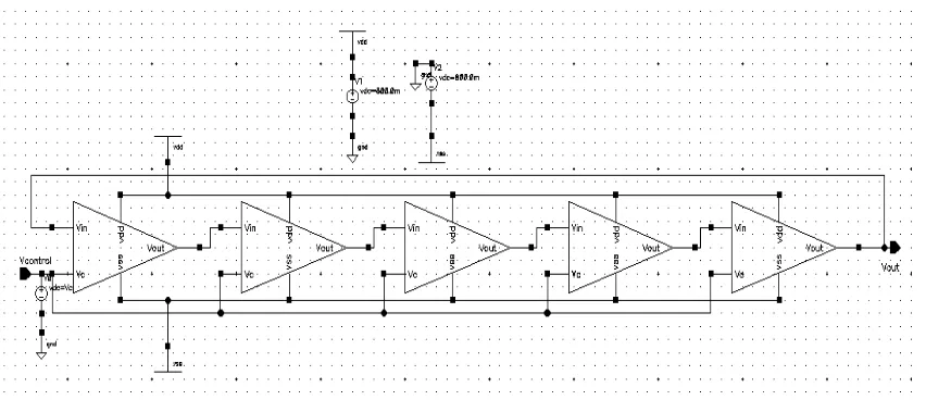
The five stages proposed ring oscillator consists of five delay cell cascaded and output is then feedback to the input of first stage. Control voltage from 0V to 1V is provided by dc voltage source. Control voltage is directly feed to the pass transistor NMOS M4 (see in Fig. 4). Vin and Vout are the two single ends of the unit delay cell and thus all the five stages are connected as shown in Fig. 3. The proposed pass transistor VCO block diagram is shown in Fig. 4. This VCO is fully design in cadence UMC .18µm CMOS technology. The supplied Vdd is 0.8V and the Vss is -0.8V.
Fig. 3 Proposed Five stage single ended ring oscillator block diagram
Figure 4 shows the schematic diagram of the five stage VCRO. The circuit is designed such that the rise and fall time is equal and gives the better transient performance. The oscillation frequency can be calculated by calculating each delay cell’s delay time (t).
Fig. 4 proposed five stage single ended ring oscillator circuit diagram
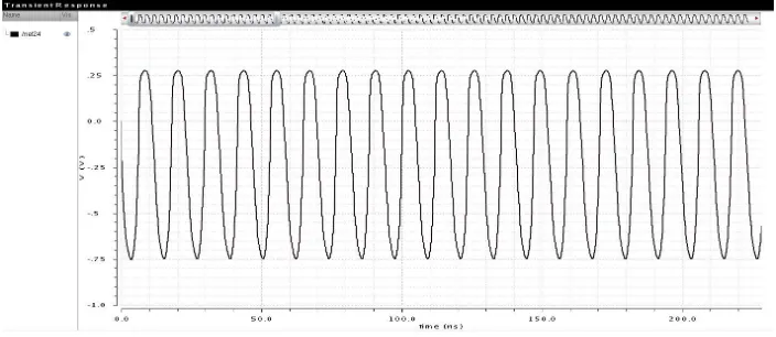
Fig. 5 Transient output of each delay cell
The transient outputs of the proposed VCO are shown in figure 5 and figure 6. Fig. 5 shows the transient waveform of each five delay cell output. Each output of the delay cell is delayed by certain value and thus the final time delay of the overall circuit is Td = N×t .Where N is the number of delay cells and t is the time delay of each stage. Figure 6 shows the transient output of the final (fifth delay stage output) delay stage.
Fig. 6 Transient output of VCRO
IV.SIMULATION RESULTS
ISSN(Online): 2320-9801
ISSN (Print) : 2320-9798
I
nternational
J
ournal of
I
nnovative
R
esearch in
C
omputer
and
C
ommunication
E
ngineering
(An ISO 3297: 2007 Certified Organization)
Vol. 4, Issue 7, July 2016
Fig. 7Phase noise at various Vc (Control voltage)
The phase noise at 1MHz offset is calculated by is -117.92dBc/Hz. The phase noise variations according to the control voltage can be seen in figure 7. Figure 8 shows the Frequency voltage characteristic of the designed VCRO. It can be seen that the Frequency voltage curve is linear and can be used for various applications. The control voltage varies from 0V to 800mV and at this control voltage band the frequency tuning range varies from 71MHz-112MHz.
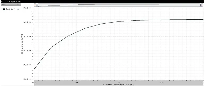
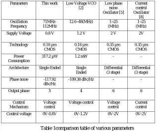
Power dissipation at various control voltage is shown in figure 9. At control voltage equal to 0V the power dissipation is around 313µW and at highest control voltage that is at .8V the power dissipation becomes saturate at 317.2µW. It can be seen from the result that the proposed design is a low power voltage control ring oscillator design. Table 1 shows comparison of proposed VCO parameters to the referenced parameters. The designed VCO is quite good in frequency, power dissipation and phase noise parameters. It can be seen in the Table 1.
Table 1comparison table of various parameters
It is seen that there is trade-off between frequency and phase noise. If the number of delay stages is increased the phase noise is reduced. But at every increase in the delay cell the frequency became extremely decreases. If we want to work with specific kind of frequency then we have to compromise with the phase noise and wise versa. Taking about power dissipation, it is also increases as the stage are increasing. Therefore there should be as minimum stages as possible.
Fig. 10comparative analysis of the Kvco curve at different number of delay cells
0 200 400 600 800
0 0.1 0.2 0.3 0.4 0.5 0.6 0.7 0.8 0.9 1
Fr e q u e n cy (M H z)
Control Voltage (V)
Nine Stage vco
Five Stage vco
Three Stage vco
Parameters This work Low Voltage VCO
[2] Low phase noise Oscillator [5] Current control Oscillator [8] Oscillation Frequency 71MHz-112MHz
12.6~48(MHz) 1~25
(MHz)
1~25 (MHz)
Supply Voltage 0.8 V 1.2 V 2 V 2V
Technology 0.18 µm
CMOS 0.18 µm CMOS 0.35 µm CMOS 0.35 µm CMOS Power Consumption
317.2 µW 1.2 mW - -
Architecture Single Ended Single
Ended
Differential (3 stage)
Differential (3 stage)
Phase noise -117.92
dBc/Hz
-109.38 dBc/Hz - -
Output phase 5 4 6 6
Control Mechanism
Voltage control
Voltage control Voltage
control
Current control
ISSN(Online): 2320-9801
ISSN (Print) : 2320-9798
I
nternational
J
ournal of
I
nnovative
R
esearch in
C
omputer
and
C
ommunication
E
ngineering
(An ISO 3297: 2007 Certified Organization)
Vol. 4, Issue 7, July 2016
For the optimization of the phase noise, power dissipation and the frequncy range we have used the five stage delay cell structure. The comparative analysis of the frequency verses control voltage at different number of delay cells can be seen in the figure 10. Figure 10 shows the relative results and that is why there is difference of phase noise in each type of delay stage design VCO topology. But we have optimised the sizing of all CMOS and observed that five stage ring oscillator can be work at lower phase noise and good frequency range.
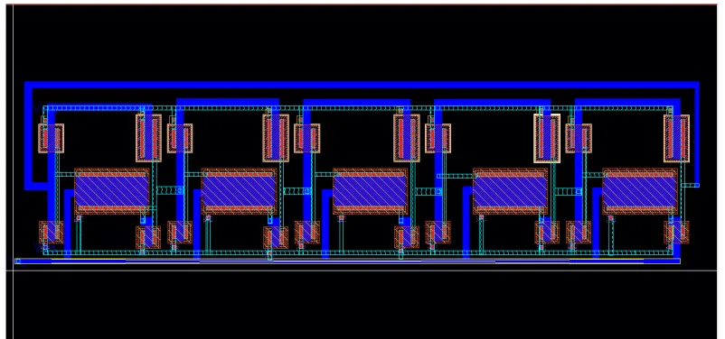
Fig. 11Layout of five stage ring oscillator
V. CONCLUSION AND FUTURE WORK
The simulation results shows that the designed CMOS VCRO noise is good compared to the other VCRO and thus we can use this oscillator in various applications such as FM radio telecommunication. Apart from the noise the designed VCRO is a low power dissipation oscillator. The proposed design supports us to use these two parameters efficiently and thus maximizes the figure of merit.As the performance of the proposed VCRO is analyzed between different numbers of stages, so in future with some modifications in design considerations the performance of the proposed VCRO can be Increase. We have used the pass transistor delay cell, as the type of frequency tuning and number of stages change, the complexity and the performance will change. We can increase the number of stages to improve phase noise but the frequency of oscillation will decrease.
REFERENCES
1. Young-Shig Choi,‘A Negative Feedback Looped Voltage-Controlled Ring Oscillator With Frequency Voltage Converter’ IEEE transactions on microwave theory and techniques, vol. 61, no. 9, pp.3271-3276, September 2013
2. San-Fu Wang, ‘Low-Voltage, Full-Swing Voltage-Controlled Oscillator with Symmetrical Even-Phase Outputs Based on Single-Ended Delay Cells,’ IEEE transaction very large scale integration (VLSI) system vol. 23 no. 9,pp.1801-1807,September 2015
3. T.D. Loveless, L.W. Massengill, W.T. Holman, and B.L. Bhuva,‘Modeling and Mitigating Single-Event Transients in Voltage-Controlled Oscillators’ IEEE transactions on nuclear science, vol. 54, no. 6, pp.2561-2567, December 2007
4. Stephen Docking andManojSachdev,‘An Analytical Equation for the Oscillation Frequency of High-Frequency Ring Oscillators’ IEEE journal of solid-state circuits, vol. 39, no. 3,pp.533-537, March 2004
5. Prakash Kumar Rout,DebiprasadPriyabrataAcharya, and Ganapati Panda, ‘A Multiobjective Optimization Based Fast and Robust Design Methodology for Low Power and Low Phase Noise Current Starved VCO’ IEEE Transactions on semiconductor manufacturing, vol. 27, no. 1,pp.43-50, February 2014.
6. Y. Boulghassoul, L.W. Massengill, A.L. Sternberg, and B. L. Bhuva,‘Effects of Technology Scaling on the SET Sensitivity of RF CMOS Voltage-Controlled Oscillators’ IEEE transactions on nuclear science, vol. 52, no. 6,pp.2426-2432, December 2005
9. R. chebli, X. Zhao and M. SawanPolySTIMNeurotechnologies Laboratory, ‘A Wide Tuning Range Voltage-Controlled Ring Oscillator dedicated to Ultrasound Transmitter’Department of Electrical Engineering, ÉcolePolytechnique de Montréal robert.chebli, pp.01-07, 2004 10. YuxianOu, Nathen Barton, RaduFetche, NilakantanSeshan, Terri Fiez, Un-Ku Moon, and KartikeyaMayaram‘Phase Noise Simulation and
Estimation Methods: A Comparative Study’ IEEE transactions on circuits and systems—ii: analog and digital signal processing, vol. 49, no. 9, pp.635-638,September 2002
11. Thomas H. Lee and Ali Hajimiri, ‘ Oscillator Phase Noise: A Tutorial’ IEEE journal of solid-state circuits, vol. 35, no. 3,pp.326-336, March 2000
BIOGRAPHY