Bandwidth and SNR Analysis of 4
th
order
VCO- Based ADC using Phase Detector as a
Loop Filter
Abhishek Kumar Prajapati1, Ayoush Johari2
M.Tech Student, Dept. of Electronics & Communication Engineering, Rajeev Gandhi Proudyogiki Vishwavidyalaya, Lakshmi Narain college of Technology and Science, Bhopal, India1
Assistant Professor, Dept. of Electronics & Communication Engineering, Rajeev Gandhi Proudyogiki Vishwavidyalaya, Lakshmi Narain College of Technology and Science, Bhopal, India2
ABSTRACT: This paper presents the bandwidth and SNR analysis of 4th order VCO based ADC. The 4th order
VCO-ADC has been explored on 50 nm MOCMOS technology which measures SNR of 74 dB over 127 GHz frequency using 5V supply. The noise shaping has been done by putting the quantization error in the feedback loop.
KEYWORDS : VCO based ADC; SNR; Bandwidth; noise shaping
I. INTRODUCTION
In the mixed signal category, the converter plays a important role in the signal conversion i.e. changing analog signal to digital or vice-versa. The analog to digital converters are called as ADC and the digital to analog converters are called as DAC. VCO is one of the most important basic building blocks in analog and digital circuit. One of the most promising analog to digital converter (ADC) architectures now a days is the VCO based ADC. The ring VCO based time-domain delta-sigma ADC has many promising advantages compared with the conventional voltage-based ones, such as an order of magnitude reduction in chip area, a high DC gain and a reduced design complexity by replacing many circuit blocks such as the integrators, digital to analog converters (DAC), quantizer by only a ring VCO and some standard digital blocks. Besides these advantages, there are also inevitable drawbacks. The primary one is the severe nonlinearity of the
Kv (the voltage to frequency conversion coefficient of the VCO), which limits the linearity of the circuit as well as the output signal.
A VCO has two traits that are especially attractive and relevant in the design of Continuous time sigma-delta ADC’s i.e.
CT ΔΣ ADC’s. First, the VCO behaves as a CT voltage-to-phase integrator. Second one is the digital nature of a
ring-VCO’s outputs. While the VCO output phase and frequency are continuously varying, the VCO output itself toggles between two discrete levels, VDD and GND, much like a CMOS digital gate. A serious drawback of this multi-phase approach, however, is that the counter becomes proportionately more complicated to design, and typically consumes greater power and area in order to meet timing and data throughput constraints. At the same time, both the single phase and multi-phase VCO-based ADC must contend with error incurred when the counter misses a VCO edge during reset. VCO based ADC suffers with severe non-linearities which limits the noise shaping property of the signal which results in the less SNR value of the circuit. The value of the SNR increases with the increase in the order of the VCO-ADC circuit. With the increased VCO-ADC order certain non-linearities gets eliminated .
II. BACKGROUND
than frequency is used as the key output variable of the quantizer. In practice, thermal noise, DAC mismatch, and other noise and error terms will add on top of the quantization noise floor and further degrade SNDR.
In order to achieve the performance target of SNDR 70dB, it is necessary to achieve higher order quantization noise shaping by extending the loop filter beyond first-order. The nonlinearity in the VCO’s voltage-to-frequency (Kv) transfer characteristic seriously limits the resolution of VCO-based ADCs as shown in Fig. 1. The nonlinearity in the VCO’s voltage-to-frequency (Kv) transfer characteristic seriously limits the resolution of VCO-based ADCs as its clear in Fig. 1. While the circuit in Fig. 2 improves distortion performance by placing a high-gain filter before the VCO and employing negative feedback, Kv nonlinearity still limits resolution to less than 11 ENOB in a 20MHz bandwidth. The resolution of prior VCO based ADC’s was primarily limited by distortion arising from the VCO Kv non-linearity. While negative feedback techniques helped to suppress the distortion by more than an order of magnitude, non-linearity still prevented the ADC from achieving its full dynamic range.
The work in [6],[8],[9] shows how the linearity of the circuit was limited by severe non-linearities, which limits the linearity of the published designs to mostly between 30- 50dB. A continuous time delta sigma (CT-ΔΣ) architecture proposed in [11] achieved second order noise shaping by preceding the multi-phase VCO quantizer with an op-amp
based integrator, and using a multi-bit feedback DAC. The Discrete time(DT) ΔΣ architecture in [12] tried to bypass a
However, this approach had additional complexities in the frequency difference detector design, and lost the inherent first-order noise-shaping provided by the VCO quantizer. A modified version of the ADC in [13] was actually implemented and provided measured results in [14]. Ref [14] shows that the third-order CT ΔΣ ADC achieved an extra
order of noise shaping without a second op-amp integrator by creating a passive pole with a large on-chip capacitor. Fig 1 shows the third order noise shaping of VCO-ADC. Noise shaping works by putting the quantization error in a feedback loop because any feedback loop functions as a filter, so by creating feedback loop for error itself, the error can be filtered as desired.
III. 4TH
ORDER VCO BASED ADC
The 4th order VCO based ADC [12] exhibits the SNR value of greater than 70 dB. In [12] the circuit is implemented using VCO quantizer, RZ DAC, NRZ DAC, and the loop filter. The quantization error has been feedback through the closed loop system to make the noise shaping property of the circuit better. The loop filter is made tunable to obtain the desired frequency response. The feedback path is implemented as a feedback DAC by using either NRZ or RZ DAC. RZ DAC is used within the minor loop feedback since any quantization noise folding arising from VCO Kv
non-linearity will be suppressed by the open loop gain of the loop filter. The result showed the SNR value of 81.2 dB over 20 MHz bandwidth. The resolution of an ADC is specified by the number of bits used to represent analog value, in principle giving 2N signals for an N-bit signal. Effective number of bits i.e. ENOB is the measure of the ADC and its associated circuitry. This paper presents the work which deals with the ENOB=12. In order to achieve SNR > 70 dB it is necessary to achieve higher order quantization nose shaping by extending the loop filter.
IV. CIRCUIT DESIGN AND SIMULATIONS
Likewise in [12] instead of increasing the loop filter order the presented work uses PD i.e. phase detector as a loop filter with the simplified RZ DAC and NRZ DAC configurations. PD generates an output signal whose phase is related to the phase of an input signal. Keeping the input and output phase in lock step also implies keeping the input and output frequency the same.
A. PHASE DETECTOR
The phase detector here compares the two input signals and produces an error signal which is proportional to their phase difference. The error signal is low pass filtered and used to drive a VCO which creates output phase. The basic schematic of the phase detector is shown in the Fig. 5.
B. RZ DAC
Due to its heightened sensitivity to clock jitter RZ DAC is used as a minor feedback loop. RZ DAC is a delay
Fig 7. Schematic diagram of RZ DAC Fig 8. Schematic representation of VCO integrator and quantizer
compensating DAC in order to absorb the propagation delay of the quantizer as shown in Fig. 5. RZ DAC has effectively twice the bandwidth of its NRZ counterpart, requiring high power DAC switch buffers. Errors in the minor-loop DAC are suppressed by the gain of the PD.
C. NRZ DAC
The multibit NRZ DAC structure as shown in Fig. 7. is adopted as a main feedback loop so that the converter can be made less sensitive to clock jitter. The mismatches in minor loop DAC are not as serious as those in main NRZ feedback DAC, thanks to the phase detector gain.
D. VCO Quantizer
The VCO delay element in VCO quantizer is based on the current starved inverter from [16] , and enables full swing output signals of the output frequency. Current steering RZ and NRZ DAC are implemented for their fast switching speeds. The SNR degradation due to clock jitter can be reduced significantly by pursuing a multibit quantizer and NRZ feedback DAC implementation [13],[14],[15],[16].
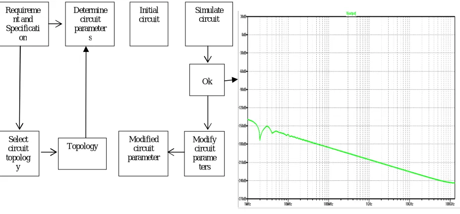
V. METHODOLOGY USED
Fig 9. Design procedure and methodology for various topologies of Fig 10. FFT plot of 4th order VCO-ADC using phase detector as a sensing circuits loop filter
VI. RESULT
TABLE I. PERFORMANCE ANALYSIS OF DIFFERENT ORDERS VCO BASED ADC AND THE PRESENTED WORK.
VCO-ADC type
2nd order
ADSM
2nd order
ADC ( ADSM+ VCO)
2nd order
VCO-ADC with feedback
loop
4th order
VCO-ADC Presented Work Technology 90 nm CMOS
90 nm CMOS 0.18 µm 1P5m digital CMOS
0.13 µm IBM CMOS
50 nm MOCMOS Supply
voltage 1 V 1 V 1.8 V --- 5 V
Bandwidth 20MHz 20 MHz 1 MHz 20 MHz 127 GHz
Sampling
frequency 560MHz 640 MHz 800 MHz 900MHz
---
SNR 68.4 dB 46.2 dB 60 dB 81.2 dB
74 dB
SNDR 67.3 dB 46 dB 39 dB 78.1 dB
The simulation and the FFT analysis of the above presented prototype has been performed on the LTspice simulator and the result is shown in Fig. 10. The tabular representation comparing different parameters of all the priors work has been compared in the Table I below. This work mainly focuses on the bandwidth and the SNR calculation. By creating the above prototype of 12-bit we have succeeded in achieving SNR>70 dB and the output more free from noise, as this was the main objective of our work.
VII. ACKNOWLEDGMENT
We would like to express our intense gratitude to Prof. Ayoush Johari, Asst. Prof. LNCT Group of Institutions, Bhopal for his guidance and motivation. We are also indebted to Department of Electronics and Communication Engineering, LNCT Group of Institutions. We would like to thank Prof. Dr. Soni Changlani and Dr. Rita Jain, Head of the Department, Electronics and Communication Engineering, LNCT Group of Institutions for their beneficial and constant supervision.
VIII. CONCLUSION
In this paper we have presented the 12-bit 4th order VCO based ADC using phase detector as a loop filter using 50nm MOCMOS technology. With the presented prototype we have achieved SNR value of 74 dB over 127 GHz bandwidth. The SNR with such a value supposed to have output free from noise. With this circuit we have also achieved the output free from non-linearities as compared with all the previous VCO-ADC designs.
REFERENCES
1.Hernadez, L. Electron. Technol. Dept., Carlos III Univ. of Madrid, Leganes, Spain Gutierrez, E. “Analytical Evaluation of VCO-ADC Quantization Noise Spectrum Using Pulse Frequency Modulation” Signal Processing Letters, IEEE vol.22, Issue:2, pp. 249 – 253, Feb. 2015 2.Min Park, and M.H. Perrott. “A VCO-based analog-to-digital converter with second-order Sigma-Delta noise shaping.” Circuits and Systems,
2009. ISCAS 2009. IEEE International Symposium on. 2009. pp. 3130-3133, May. 2009
3.Peng Gao; ESAT-MICAS, Katholieke Univ. Leuven , Belgium; Xinpeng Xing: Creaninckx J. ; Gielen G.” Design of an int-rinsically-linear double-VCO-based ADC with 2nd-order noise shaping” Design, Automation & Test in Europe Conference Test in Europe Conference & Exhibition (DATE), 2012, IEEE, pp. 1215 – 1220, March 2012
4.Daniels, J.;AT EL, “A 0.02mm265nm CMOS 30MHz BW all-digital differential VCO-based ADC with 64 dB SNDR”, VLSI circuits (VLSIC), 2010 IEEE Symposiumon, Vol., no., pp. 155-156, June 2010
5.Park, M.; Perrott, M.H.; , "A 78 dB SNDR 87 mW 20 MHz Bandwidth Continuous-Time sigma delta ADC With VCO-Based Integrator and Quantizer Implemented in 0.13 m CMOS," Solid-State Circuits, IEEE Journal of , vol.44, no.12, 344-3358, Dec. 2009
6.Taylor, G.; Galton, I.; , "A Mostly-Digital Variable-Rate Continuous- Time Delta-Sigma Modulator ADC," Solid-State Circuits, IEEE Journal of , vol.45, no.12, pp.2634-2646, Dec. 2010
7.Jaewook Kim; at el, "Analysis and Design of Voltage-Controlled Oscillator Based Analog-to-Digital Converter," Circuits and Systems I: Regular Papers, IEEE Transactions on , vol.57, no.1,Jan. 2010
8.A. Iwata, N. Sakimura, M. Nagata, and T. Morie. The Architecture of Delta Sigma Analog-to-Digital Converters Using a Voltage-Controlled Oscillator as a Multibit Quantizer. IEEE Trans. On Circuits and Systems II, 46(7):941–945, July 1999
9.R. Naiknaware, H. Tang, and T. S. Fiez. Time-Referenced Single-Path Multi-Bit ADC using a VCO-Based Quantizer. IEEE Trans. On Circuits and Systems II, 47(7):596–602, July 2000.
10. A. Iwata, N. Sakimura, M. Nagata, and T. Morie. The Architecture of Delta Sigma Analog-to-Digital Converters Using a Voltage-Controlled Oscillator as a Multibit Quantizer. IEEE Trans. On Circuits and Systems II, 46(7):941–945, July 1999.
11. Matthew Park and Michael H. Perrott,” A 78 dB SNDR 87 mW 20 MHz Bandwidth Continuous-Time _ ADC With VCO-Based Integrator and Quantizer Implemented in 0.13 m CMOS” IEEE JOURNAL OF SOLID-STATE CIRCUITS, VOL. 44, NO. 12, DECEMBER 2009
12. S. Yan and E. Sanchez-Sinencio. A Continuous-Time Modulator With 88-dB Dynamic Range and 1.1-MHz Signal Bandwidth. IEEE J.
Solid-State Circuits, 39(1):75–86, January 2004.
13. W. Yang, W. Schofield, H. Shibata, S. Korrapati, A. Shaikh, N. Abaskharoun, and D. Ribner. A 100mW 10 MHz-BW CT ΔΣ Modulator
with 87dB DR and 91dBc IMD. In IEEE ISSCC Dig. Tech. Papers, 2008.
14. R. Schoofs, M. Steyaert, and W. Sansen. A Design-Optimized Continuous-Time Delta-Sigma ADC for WLAN Applications. IEEE Trans.
Circuits Syst. I, Reg.Papers, 54(1):209–217, January 2007.
15. G. Mitteregger, C. Ebner, S. Mechnig, T. Blon, C. Holuigue, and E. Romani. A 20 mW 640-MHz CMOS Continuous-Time Sigma-Delta
ADC with 20-MHz Signal Bandwidth, 80-dB Dynamic Range, and 12-bit ENOB. IEEE J. Solid- State Circuits, 41(12):2641–2649, December 2006
16. M. Z. Straayer and M. H. Perrott. A 12-bit 10-MHz Bandwidth, Continuous-Time Sigma-Delta ADC With a 5-bit, 950 MS/S VCO-based