Total Harmonic Distortion Analysis of Voltage
Source, Current Source and Z-Source Inverter
Srinivas.P1, Kruthi Jayaram2
M.Tech Student, Dept of EEE, BNMIT, Bangalore, India1
Assistant Professor, Dept of EEE, BNMIT, Bangalore, India 2
ABSTRACT: This paper presents the analysis of z source inverter using boost converter as the medium to buck-boost the voltage from a dc supply. Z source converter has impedance network consisting of two inductors and two capacitors cross connected in X –shape which couples inverter main circuit to dc source. Along with normal operating states, z source inverter has an extra state known as shoot through state which allows the buck-boost operation in a single stage. A comparison between single phase VSI, CSI and ZSI is shown which shows that fundamental output voltage is higher for ZSI through shoot through. The simulation results are presented for various modulation indexes and compared with the simulation results of VSI and CSI. The results validate the effectiveness of ZSI over VSI and ZSI.
KEYWORDS: Current source inverter, Voltage source inverter, Z source inverter, modulation index, THD.
I.INTRODUCTION
VOLTAGE SOURCE INVERTER:
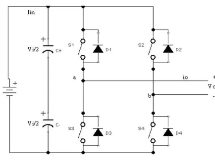
Fig 1: Single phase Voltage source inverter
Fig.1 shows such circuit where a single dc supply has been split in two halves. In such circuits the voltages across the two capacitors may not remain exactly balanced due to mismatch in the loading patterns or mismatch in leakage currents of the individual capacitors. Also, unless the capacitors are of very large magnitude, there may be significant ripple in the capacitor voltages, especially at low switching frequencies.
These topologies require only a single dc source and for medium output power applications (‘Vi’ is the input dc supply and) a large dc link capacitor (Cdc) is required across the supply terminals. Capacitors and switches are connected to dc bus using short leads to minimize the stray inductance between the capacitor and the inverter switches. In the voltage source inverter the voltage remains constant with variations in the load. It is capable of supplying variable voltage for speed control of induction motor. Both the switches S1 and S2 or S3 and S4 cannot be simultaneously operated because short circuit across the dc link voltage Vi would be produced. There are four defined and one undefined state. The undefined state is avoided, in order to avoid the short circuit across the dc bus and the undefined ac output voltage condition. The modulating technique should ensure that either the top or the bottom switch of each leg is on at any instant. It can be observed that the ac output voltage can take values up to the dc link value Vi. Several modulating techniques have been developed that are applicable to the VSIs. Among them sinusoidal PWM technique is considered for VSI.
CURRENT SOURCE INVERTER:
The circuit of a Single-phase Current Source Inverter (CSI) is shown in Fig. 2. A constant current source is assumed here, which may be realized by using an inductance of suitable value, which must be high, in series with the current limited dc voltage source. The thyristor pairs, Th1& Th3, and Th2& Th4, are alternatively turned ON to obtain a nearly square wave current waveform. Two commutating capacitors -C1in the upper half, and C2in the lower half, are used. Four diodes, D1-D4are connected in series with each thyristor to prevent the commutating capacitors from discharging into the load. The output frequency of the inverter is controlled in the usual way, i.e., by varying the half time period, (T/2), at which the thyristor in pair are triggered by pulses being fed to the respective gates by the control circuit, to turn them ON. The inductance (L) is taken as the load in this case, the reason(s) for which need not be stated, being well known. At time, t = 0, thyristor pair, Th1& Th3, is triggered by pulses at the gates. The conducting thyristor pair, Th2&Th4, is turned OFF by application of reverse capacitor voltages. Now, thyristor pair, Th1& Th3, conducts current (I). The current path is through Th1, C1, D1, Load, C2, D3, Th3, and source, I. Similarly the when the thyristor pairs, Th2 &Th4, is triggered by the pulses at the gates. The conducting thyristor pair Th1&Th3 is turned OFF by the application of reverse capacitor voltages. Now, thyristor pair, Th2 & Th4, conducts current (I). The current path is through T2, D2, C1, Load, C2, D4, T4. The output frequency of the inverter is controlled in the usual way, i.e., by varying the half time period, (T/2), at which the thyristor in pair are triggered by pulses being fed to the respective gates by the control circuit, to turn them ON. The R, RL, Motor load is considered for analyzing the performance of the given CSI.
Z-SOURCE INVERTER:
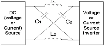
Fig 3: Z-source inverter
Z-source inverter (ZSI) which is based on Z-source network can be used to buck and boost the output AC voltage, which is not possible using traditional voltage source or current source inverters. Also the ZSI has the unique ability to short the dc link, which is not possible in the traditional voltage source inverters. This improves the reliability of the circuit .Actually concept of boosting the input voltage is based on the ratio of “shoot-through” time to the whole switching period. Z-source converter is shown in Fig.6 where an impedance network is placed between d.c. link and inverter. Z-source inverter (ZSI) provides a greater voltage than the D.C. link voltage. It reduces the inrush current & harmonics in the current because of two inductors in z source network. It forms a second order filter &handles the undesirable voltage sags of the D.C. voltage source.
Fig.3 shows a topology of the single phase Z-source inverter, where the impedance network is placed between the power source and the single phase inverter The presence of 2 inductors & 2 capacitors in Z-source network, allows both switches of same phase leg ON state simultaneously, called as shoot-through state & gives boosting capability to the inverter without damaging the switching devices. During shoot through state energy is transferred From capacitor To inductor & hence Z-source inverter(ZSI) gains the voltage boosting capability Diode is required to prevent the discharge of overcharged Capacitor through the source.
II.EQUIVALENT CIRCUIT AND OPERATING PRINCIPLE
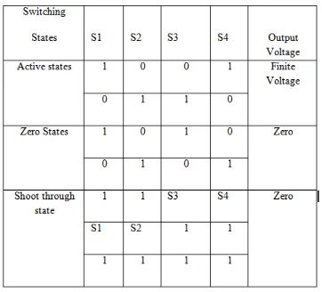
cannot provide such feature. The main feature of the Z-source is implemented by providing gate pulses including the shoot-through pulses. Here how to insert this shoot through state becomes the key point of the control methods. It is obvious that during the shoot-through state, the output terminals of the inverter are shorted and the output voltage to the load is zero. The output voltage of the shoot through state is zero, which is the same as the traditional zero states, therefore the duty ratio of the active states has to be maintained to output a sinusoidal voltage, which means shoot-through only replaces some or all of the traditional zero states.
Let us briefly examine the Z-source inverter structure. In Fig.3, the three-phase Z-source inverter bridge has nine permissible switching states (vectors) unlike the traditional three-phase V-source inverter that has eight. The traditional three-phase V-source inverter has six active vectors when the DC voltage is impressed across the load and two zero vectors when the load terminals are shorted through either the lower or upper three devices, respectively. However, three-phase Z-source inverter bridge has one extra zero state (or vector) when the load terminals are shorted through both the upper and lower devices of any one phase leg (i.e., both devices are gated on),any two phase legs, or all three phase legs. This shoot-through zero state (or vector) is forbidden in the traditional V-source inverter, because it would cause a shoot-through. We call this third zero state (vector) the shoot-through zero state (or vector), which can be generated by seven different ways: shoot through via any one phase leg, combinations of any two phase legs, and all three phase legs.
The Z-source network makes the shoot-through zero state possible.
This shoot-through zero state provides the unique buck-boost feature to the inverter. The Z-source inverter can be operated in three modes which are explained in below.
SWITCHING STATES:
Table 1 Switching States of Single Phase ZSI
OPERATING MODES:
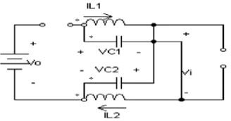
Mode 1: The circuit is in a shoot-through zero state, the sum of the two capacitor voltage is greater than the DC source voltage (VC1+VC2 > V0), the diode is reverse biased, and the capacitors charge the inductors. The voltages across the inductors are:
VL1 = VC1, VL2 =VC2.
The dc-link voltage across Inverter Bridge during non shoot through interval (T1) is VI=VC-VL=2VC-VDC………. (3)
Mode 2: The Inverter is in a non-shoot through state (one of the 6 active states and 2 traditional zero states) and the inductor current meets the following in the equation,
IL > (1/2)*Ii
Again because of the symmetry of the circuit, the capacitor current IC1 and IC2 and the inductor current IL1 and IL2 should be equal to each other respectively. In this mode, the input current from the DC source becomes
Iin = IL1 + IC1 = IL1 + (IL2 - Ii) = 2IL- Ii > 0
Therefore, the diode is conducting and the voltage across the inductor is VL = V0 - VC
Which is negative (the capacitor voltage is higher than the input voltage during boost operation when there is shoot through states), thus the inductor current decreases linearly assuming the capacitor voltage is constant. As time goes on, the inductor current keeps decreasing to a level that no longer can be met. At this point, the input current in or the diode current is decreased to zero, Mode 2 ends and the inverter enters to a new mode.
Mode 3: The inverter is in one of the 6 active states, and at the end of Mode 2, the inductor current decreases to half of the inverter DC side current, Ii. As a result, the input current becomes zero and the diode becomes reverse-biased. Assuming that the inverter load is inductive and has a much larger inductance than that of the inductor L1 and L2, the inductance of L1 and L2 are negligible and the inductor current and inverter voltage VI are respectively.
IL = (1/2)*Ii and VI = VC
Mode 4: The inverter is in one of the 2 traditional zero states (Ii=0) and at the end of Mode 2, the inductor current decreases to zero, thus a new operation mode appears. In Mode 4, the diode stops conducting and the inverter is an open circuit to the Z-source network because of Ii=0. The inductor current becomes zero and maintains zero until the next switching action. Therefore in this mode, the Z-source circuit is isolated from both the DC source and the load.
Mode 5: The inverter is switched to an active state after one of the traditional zero states. The inductor current may decrease to a level that is less than half Ii. After switched to an active state, the inverter cannot enter the active state immediately because that the inductor current is smaller than half of the inverter DC current (the condition of (2) does not hold true) and the inverter enters a freewheeling state described in Fig (e).The two diodes in the equivalent circuit are the free -wheeling diodes of the inverter phase legs. This diode free- wheeling state turns the inverter into a shoot through zero state. During this shoot through zero state, all the equations of Mode 1 hold true and the inductor current increases linearly. This mode continues until the inductor current increases to half of the DC side current to the inverter. And the Z-source circuit enters Mode 3 and the inverter enters the intended active state. The difference between this mode and Mode 1 is that this mode is not intentionally created by the control signal and depends on the load current and the inductor current at the time of switching with different control methods and different circuit parameters and load.
IV. SIMULATION RESULTS
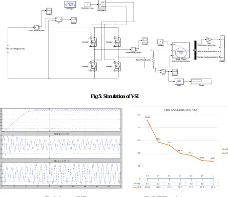
VOLTAGE SOURCE INVERTER:The simulation and results for VSI using MATLAB is given below
Fig 5: Simulation of VSI
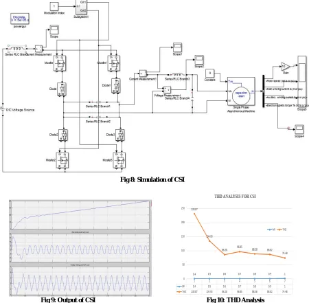
CURRENT SOURCE INVERTER:
The simulation and results for CSI using MATLAB is given below
Fig 8: Simulation of CSI
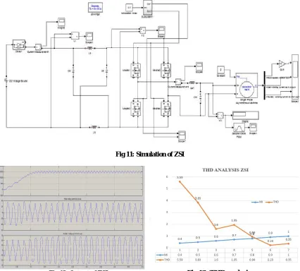
Z-SOURCE INVERTER:
The simulation and results for ZSI using MATLAB is given below
Fig 11: Simulation of ZSI
FFT analysis report of VSI, CSI, ZS
V. CONCLUSION
This paper presented the analysis of z source inverter using buck-boost converter as the medium to buck-boost the voltage from a dc supply. The analysis of comparing VSI, CSI and ZSI was done. Shoot through analysis was explained with respect to the ZSI topology. Simulation circuits and results were explained with proper variation in the modulation index the THD analysis was also noted.
REFERENCES
[1] Fang Zheng Peng, “Z-Source Inverter”, IEEE Transaction Industrial Application. Vol.-39, No.-2, Page: 504-510, 2003
[2] Fang Zheng Peng, “Z-Source Inverter for Motor Drives”, IEEE Transaction on Power Electronics. Vol.-20, No.-4, Page: 857-863, 2005. [3] Sattyendrasing A.Seragi “Review on Z-source Inverter” International Journal of Computer Applications (1975-8887)